RAiO RA8806 - Display Future
RAiO RA8806 - Display Future
RAiO RA8806 - Display Future

You also want an ePaper? Increase the reach of your titles
YUMPU automatically turns print PDFs into web optimized ePapers that Google loves.
Version 1.3<br />
<strong>RA8806</strong><br />
Two Layers Character/Graphic LCD Controller<br />
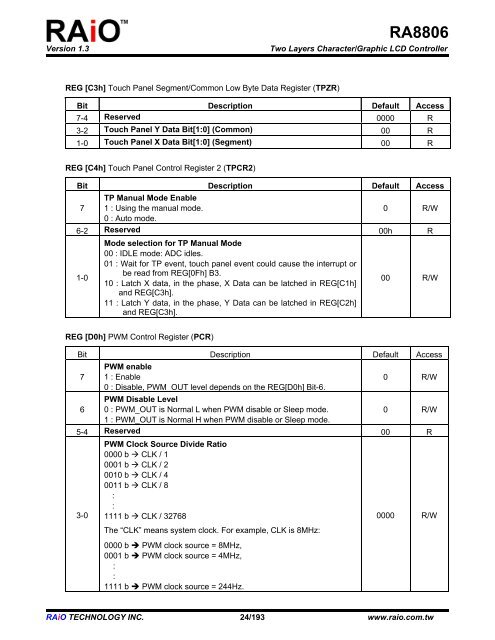
REG [C3h] Touch Panel Segment/Common Low Byte Data Register (TPZR)<br />
Bit Description Default Access<br />
7-4 Reserved 0000 R<br />
3-2 Touch Panel Y Data Bit[1:0] (Common) 00 R<br />
1-0 Touch Panel X Data Bit[1:0] (Segment) 00 R<br />
REG [C4h] Touch Panel Control Register 2 (TPCR2)<br />
Bit Description Default Access<br />
7<br />
TP Manual Mode Enable<br />
1 : Using the manual mode.<br />
0 R/W<br />
0 : Auto mode.<br />
6-2 Reserved 00h R<br />
1-0<br />
Mode selection for TP Manual Mode<br />
00 : IDLE mode: ADC idles.<br />
01 : Wait for TP event, touch panel event could cause the interrupt or<br />
be read from REG[0Fh] B3.<br />
10 : Latch X data, in the phase, X Data can be latched in REG[C1h]<br />
and REG[C3h].<br />
11 : Latch Y data, in the phase, Y Data can be latched in REG[C2h]<br />
and REG[C3h].<br />
00 R/W<br />
REG [D0h] PWM Control Register (PCR)<br />
Bit Description Default Access<br />
7<br />
PWM enable<br />
1 : Enable<br />
0 R/W<br />
0 : Disable, PWM_OUT level depends on the REG[D0h] Bit-6.<br />
6<br />
PWM Disable Level<br />
0 : PWM_OUT is Normal L when PWM disable or Sleep mode.<br />
0 R/W<br />
1 : PWM_OUT is Normal H when PWM disable or Sleep mode.<br />
5-4 Reserved 00 R<br />
3-0<br />
PWM Clock Source Divide Ratio<br />
0000 b CLK / 1<br />
0001 b CLK / 2<br />
0010 b CLK / 4<br />
0011 b CLK / 8<br />
:<br />
:<br />
1111 b CLK / 32768<br />
0000 R/W<br />
The “CLK” means system clock. For example, CLK is 8MHz:<br />
0000 b PWM clock source = 8MHz,<br />
0001 b PWM clock source = 4MHz,<br />
:<br />
:<br />
1111 b PWM clock source = 244Hz.<br />
<strong>RAiO</strong> TECHNOLOGY INC. 24/193 www.raio.com.tw