

TL594 Precision Switchmode Pulse Width Modulation Control Circuit
TL594 Precision Switchmode Pulse Width Modulation Control Circuit
TL594 Precision Switchmode Pulse Width Modulation Control Circuit

You also want an ePaper? Increase the reach of your titles
YUMPU automatically turns print PDFs into web optimized ePapers that Google loves.
The <strong>TL594</strong> is a fixed frequency, pulse width modulation control<br />
circuit designed primarily for <strong>Switchmode</strong> power supply control.<br />
http://onsemi.com<br />
• Complete <strong>Pulse</strong> <strong>Width</strong> <strong>Modulation</strong> <strong>Control</strong> <strong>Circuit</strong>ry<br />
• On–Chip Oscillator with Master or Slave Operation<br />
• On–Chip Error Amplifiers<br />
• On–Chip 5.0 V Reference, 1.5% Accuracy<br />
• Adjustable Deadtime <strong>Control</strong><br />
• Uncommitted Output Transistors Rated to 500 mA Source or Sink<br />
• Output <strong>Control</strong> for Push–Pull or Single–Ended Operation<br />
• Undervoltage Lockout<br />
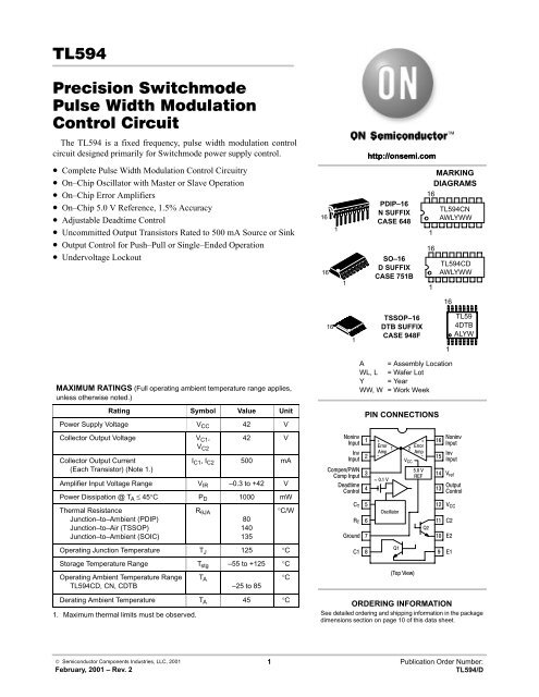
16<br />
16<br />
1<br />
1<br />
PDIP–16<br />
N SUFFIX<br />
CASE 648<br />
SO–16<br />
D SUFFIX<br />
CASE 751B<br />
MARKING<br />
DIAGRAMS<br />
16<br />
1<br />
16<br />
1<br />
<strong>TL594</strong>CN<br />
AWLYWW<br />
<strong>TL594</strong>CD<br />
AWLYWW<br />
16<br />
16<br />
1<br />
TSSOP–16<br />
DTB SUFFIX<br />
CASE 948F<br />
1<br />
TL59<br />
4DTB<br />
ALYW<br />
MAXIMUM RATINGS (Full operating ambient temperature range applies,<br />
unless otherwise noted.)<br />
Rating Symbol Value Unit<br />
Power Supply Voltage V CC 42 V<br />
Collector Output Voltage V C1 ,<br />
V C2<br />
42 V<br />
Collector Output Current<br />
(Each Transistor) (Note 1.)<br />
I C1 , I C2 500 mA<br />
Amplifier Input Voltage Range V IR –0.3 to +42 V<br />
Power Dissipation @ T A ≤ 45°C P D 1000 mW<br />
Thermal Resistance<br />
Junction–to–Ambient (PDIP)<br />
Junction–to–Air (TSSOP)<br />
Junction–to–Ambient (SOIC)<br />
R θJA<br />
80<br />
140<br />
135<br />
°C/W<br />
Operating Junction Temperature T J 125 °C<br />
Storage Temperature Range T stg –55 to +125 °C<br />
Operating Ambient Temperature Range<br />
<strong>TL594</strong>CD, CN, CDTB<br />
T A<br />
–25 to 85<br />
Derating Ambient Temperature T A 45 °C<br />
1. Maximum thermal limits must be observed.<br />
°C<br />
<br />
<br />
<br />
<br />
<br />
<br />
<br />
A = Assembly Location<br />
WL, L = Wafer Lot<br />
Y = Year<br />
WW, W = Work Week<br />
PIN CONNECTIONS<br />
<br />
<br />
<br />
<br />
<br />
<br />
<br />
<br />
<br />
<br />
<br />
<br />
<br />
<br />
<br />
<br />
<br />
≈ <br />
<br />
<br />
<br />
<br />
<br />
<br />
<br />
<br />
<br />
<br />
ORDERING INFORMATION<br />
See detailed ordering and shipping information in the package<br />
dimensions section on page 10 of this data sheet.<br />
<br />
<br />
<br />
<br />
<br />
<br />
<br />
<br />
<br />
<br />
<br />
<br />
<br />
<br />
<br />
<br />
<br />
<br />
<br />
© Semiconductor Components Industries, LLC, 2001<br />
February, 2001 – Rev. 2<br />
1 Publication Order Number:<br />
<strong>TL594</strong>/D
<strong>TL594</strong><br />
RECOMMENDED OPERATING CONDITIONS<br />
Characteristics Symbol Min Typ Max Unit<br />
Power Supply Voltage V CC 7.0 15 40 V<br />
Collector Output Voltage V C1 , V C2 – 30 40 V<br />
Collector Output Current (Each transistor) I C1 , I C2 – – 200 mA<br />
Amplified Input Voltage V in 0.3 – V CC – 2.0 V<br />
Current Into Feedback Terminal l fb – – 0.3 mA<br />
Reference Output Current l ref – – 10 mA<br />
Timing Resistor R T 1.8 30 500 kΩ<br />
Timing Capacitor C T 0.0047 0.001 10 µF<br />
Oscillator Frequency f osc 1.0 40 200 kHz<br />
PWM Input Voltage (Pins 3, 4, 13) – 0.3 – 5.3 V<br />
ELECTRICAL CHARACTERISTICS (V CC = 15 V, C T = 0.01 µF, R T = 12 kΩ, unless otherwise noted.)<br />
For typical values T A = 25°C, for min/max values T A is the operating ambient temperature range that applies, unless otherwise noted.<br />
Characteristics Symbol Min Typ Max Unit<br />
V<br />
REFERENCE SECTION<br />
Reference Voltage<br />
V<br />
(I O = 1.0 mA, T A = 25°C)<br />
(I O = 1.0 mA)<br />
ref<br />
4.925<br />
4.9<br />
5.0<br />
–<br />
5.075<br />
5.1<br />
Line Regulation (V CC = 7.0 V to 40 V) Reg line – 2.0 25 mV<br />
Load Regulation (I O = 1.0 mA to 10 mA) Reg load – 2.0 15 mV<br />
Short <strong>Circuit</strong> Output Current (V ref = 0 V) I SC 15 40 75 mA<br />
OUTPUT SECTION<br />
Collector Off–State Current (V CC = 40 V, V CE = 40 V) I C(off) – 2.0 100 µA<br />
Emitter Off–State Current (V CC = 40 V, V C = 40 V, V E = 0 V) I E(off) – – –100 µA<br />
Collector–Emitter Saturation Voltage (Note 2.)<br />
Common–Emitter (V E = 0 V, I C = 200 mA)<br />
Emitter–Follower (V C = 15 V, I E = –200 mA)<br />
V SAT(C)<br />
V SAT(E)<br />
–<br />
–<br />
1.1<br />
1.5<br />
1.3<br />
2.5<br />
V<br />
Output <strong>Control</strong> Pin Current<br />
Low State (V OC ≤ 0.4 V)<br />
High State (V OC = V ref )<br />
Output Voltage Rise Time<br />
Common–Emitter (See Figure 13)<br />
Emitter–Follower (See Figure 14)<br />
Output Voltage Fall Time<br />
Common–Emitter (See Figure 13)<br />
Emitter–Follower (See Figure 14)<br />
I OCL –<br />
I OCH –<br />
t r<br />
–<br />
–<br />
t f<br />
–<br />
–<br />
ERROR AMPLIFIER SECTION<br />
Input Offset Voltage (V O (Pin 3) = 2.5 V) V IO – 2.0 10 mV<br />
Input Offset Current (V O (Pin 3) = 2.5 V) I IO – 5.0 250 nA<br />
Input Bias Current (V O (Pin 3) = 2.5 V) I IB – –0.1 –1.0 µA<br />
Input Common Mode Voltage Range (V CC = 40 V, T A = 25°C) V ICR 0 to V CC –2.0 V<br />
Inverting Input Voltage Range V IR(INV) –0.3 to V CC –2.0 V<br />
Open Loop Voltage Gain (∆V O = 3.0 V, V O = 0.5 V to 3.5 V, R L = 2.0 kΩ) A VOL 70 95 – dB<br />
Unity–Gain Crossover Frequency (V O = 0.5 V to 3.5 V, R L = 2.0 kΩ) f C – 700 – kHz<br />
Phase Margin at Unity–Gain (V O = 0.5 V to 3.5 V, R L = 2.0 kΩ) φm – 65 – deg.<br />
Common Mode Rejection Ratio (V CC = 40 V) CMRR 65 90 – dB<br />
Power Supply Rejection Ratio (∆V CC = 33 V, V O = 2.5 V, R L = 2.0 kΩ) PSRR – 100 – dB<br />
Output Sink Current (V O (Pin 3) = 0.7 V) I O – 0.3 0.7 – mA<br />
Output Source Current (V O (Pin 3) = 3.5 V) I O + –2.0 –4.0 – mA<br />
2. Low duty cycle pulse techniques are used during test to maintain junction temperature as close to ambient temperature as possible.<br />
0.1<br />
2.0<br />
100<br />
100<br />
40<br />
40<br />
–<br />
20<br />
200<br />
200<br />
100<br />
100<br />
µA<br />
ns<br />
ns<br />
http://onsemi.com<br />
2
<strong>TL594</strong><br />
ELECTRICAL CHARACTERISTICS (V CC = 15 V, C T = 0.01 µF, R T = 12 kΩ, unless otherwise noted.)<br />
For typical values T A = 25°C, for min/max values T A is the operating ambient temperature range that applies, unless otherwise noted.<br />
Characteristics Symbol Min Typ Max Unit<br />
PWM COMPARATOR SECTION (Test <strong>Circuit</strong> Figure 11)<br />
Input Threshold Voltage (Zero Duty Cycle) V TH – 3.6 4.5 V<br />
Input Sink Current (V Pin 3 = 0.7 V) I I– 0.3 0.7 – mA<br />
DEADTIME CONTROL SECTION (Test <strong>Circuit</strong> Figure 11)<br />
Input Bias Current (Pin 4) (V Pin 4 = 0 V to 5.25 V) I IB (DT) – –2.0 –10 µA<br />
Maximum Duty Cycle, Each Output, Push–Pull Mode<br />
(V Pin 4 = 0 V, C T = 0.01 µF, R T = 12 kΩ)<br />
(V Pin 4 = 0 V, C T = 0.001 µF, R T = 30 kΩ)<br />
Input Threshold Voltage (Pin 4)<br />
(Zero Duty Cycle)<br />
(Maximum Duty Cycle)<br />
OSCILLATOR SECTION<br />
Frequency<br />
(C T = 0.001 µF, R T = 30 kΩ)<br />
(C T = 0.01 µF, R T = 12 kΩ, T A = 25°C)<br />
(C T = 0.01 µF, R T = 12 kΩ, T A = T low to T high )<br />
DC max<br />
45<br />
–<br />
V TH<br />
–<br />
0<br />
f osc<br />
–<br />
9.2<br />
9.0<br />
Standard Deviation of Frequency* (C T = 0.001 µF, R T = 30 kΩ) σf osc – 1.5 – %<br />
Frequency Change with Voltage (V CC = 7.0 V to 40 V, T A = 25°C) ∆f osc (∆V) – 0.2 1.0 %<br />
Frequency Change with Temperature<br />
(∆T A = T low to T high , C T = 0.01 µF, R T = 12 kΩ)<br />
48<br />
45<br />
2.8<br />
–<br />
40<br />
10<br />
–<br />
50<br />
–<br />
3.3<br />
–<br />
–<br />
10.8<br />
12<br />
%<br />
V<br />
kHz<br />
∆f osc (∆T) – 4.0 – %<br />
UNDERVOLTAGE LOCKOUT SECTION<br />
Turn–On Threshold (V CC Increasing, I ref = 1.0 mA)<br />
V th<br />
T A = 25°C<br />
4.0<br />
T A = T low to T high 3.5<br />
5.2<br />
–<br />
6.0<br />
6.5<br />
V<br />
Hysteresis<br />
<strong>TL594</strong>C,I<br />
<strong>TL594</strong>M<br />
V H<br />
100<br />
50<br />
150<br />
150<br />
300<br />
300<br />
mV<br />
TOTAL DEVICE<br />
Standby Supply Current (Pin 6 at V ref , All other inputs and outputs<br />
open)<br />
(V CC = 15 V)<br />
(V CC = 40 V)<br />
I CC<br />
–<br />
–<br />
Average Supply Current (V Pin 4 = 2.0 V, C T = 0.01 µF, R T = 12 kΩ,<br />
V CC = 15 V, See Figure 11) – 11 –<br />
8.0<br />
8.0<br />
15<br />
18<br />
mA<br />
mA<br />
*Standard deviation is a measure of the statistical distribution about the mean as derived from the formula, σ<br />
N<br />
Σ (X n – X) 2<br />
n = 1<br />
N – 1<br />
http://onsemi.com<br />
3
<strong>TL594</strong><br />
<br />
<br />
<br />
<br />
<br />
<br />
<br />
<br />
<br />
<br />
<br />
<br />
<br />
<br />
<br />
≈ <br />
≈ <br />
<br />
<br />
<br />
<br />
<br />
<br />
<br />
<br />
<br />
<br />
<br />
<br />
<br />
<br />
<br />
<br />
<br />
<br />
<br />
<br />
<br />
<br />
<br />
<br />
<br />
<br />
<br />
<br />
<br />
<br />
<br />
<br />
<br />
<br />
<br />
<br />
<br />
<br />
<br />
<br />
<br />
<br />
<br />
This device contains 46 active transistors.<br />
Figure 1. Representative Block Diagram<br />
<br />
<br />
<br />
<br />
<br />
<br />
<br />
<br />
<br />
<br />
<br />
<br />
<br />
<br />
<br />
Figure 2. Timing Diagram<br />
http://onsemi.com<br />
4
<strong>TL594</strong><br />
APPLICATIONS INFORMATION<br />
Description<br />
The <strong>TL594</strong> is a fixed–frequency pulse width<br />
modulation control circuit, incorporating the primary<br />
building blocks required for the control of a switching<br />
power supply. (See Figure 1.) An internal–linear sawtooth<br />
oscillator is frequency– programmable by two external<br />
components, R T and C T . The approximate oscillator<br />
frequency is determined by:<br />
f osc ≈ 1.1<br />
R T • C T<br />
For more information refer to Figure 3.<br />
Output pulse width modulation is accomplished by<br />
comparison of the positive sawtooth waveform across<br />
capacitor C T to either of two control signals. The NOR gates,<br />
which drive output transistors Q1 and Q2, are enabled only<br />
when the flip–flop clock–input line is in its low state. This<br />
happens only during that portion of time when the sawtooth<br />
voltage is greater than the control signals. Therefore, an<br />
increase in control–signal amplitude causes a corresponding<br />
linear decrease of output pulse width. (Refer to the Timing<br />
Diagram shown in Figure 2.)<br />
The control signals are external inputs that can be fed into<br />
the deadtime control, the error amplifier inputs, or the<br />
feedback input. The deadtime control comparator has an<br />
effective 120 mV input offset which limits the minimum<br />
output deadtime to approximately the first 4% of the<br />
sawtooth–cycle time. This would result in a maximum duty<br />
cycle on a given output of 96% with the output control<br />
grounded, and 48% with it connected to the reference line.<br />
Additional deadtime may be imposed on the output by<br />
setting the deadtime–control input to a fixed voltage,<br />
ranging between 0 V to 3.3 V.<br />
The pulse width modulator comparator provides a means<br />
for the error amplifiers to adjust the output pulse width from<br />
the maximum percent on–time, established by the deadtime<br />
control input, down to zero, as the voltage at the feedback<br />
pin varies from 0.5 V to 3.5 V. Both error amplifiers have a<br />
common–mode input range from –0.3 V to (V CC – 2 V), and<br />
may be used to sense power–supply output voltage and<br />
current. The error–amplifier outputs are active high and are<br />
ORed together at the noninverting input of the pulse–width<br />
modulator comparator. With this configuration, the<br />
amplifier that demands minimum output on time, dominates<br />
control of the loop.<br />
Input/Output<br />
<strong>Control</strong>s<br />
Functional Table<br />
Output Function<br />
f out<br />
f osc<br />
=<br />
Grounded Single–ended PWM @ Q1 and Q2 1.0<br />
@ V ref Push–pull Operation 0.5<br />
When capacitor C T is discharged, a positive pulse is<br />
generated on the output of the deadtime comparator, which<br />
clocks the pulse–steering flip–flop and inhibits the output<br />
transistors, Q1 and Q2. With the output–control connected<br />
to the reference line, the pulse–steering flip–flop directs the<br />
modulated pulses to each of the two output transistors<br />
alternately for push–pull operation. The output frequency is<br />
equal to half that of the oscillator. Output drive can also be<br />
taken from Q1 or Q2, when single–ended operation with a<br />
maximum on–time of less than 50% is required. This is<br />
desirable when the output transformer has a ringback<br />
winding with a catch diode used for snubbing. When higher<br />
output–drive currents are required for single–ended<br />
operation, Q1 and Q2 may be connected in parallel, and the<br />
output–mode pin must be tied to ground to disable the<br />
flip–flop. The output frequency will now be equal to that of<br />
the oscillator.<br />
The <strong>TL594</strong> has an internal 5.0 V reference capable of<br />
sourcing up to 10 mA of load current for external bias<br />
circuits. The reference has an internal accuracy of ±1.5%<br />
with a typical thermal drift of less than 50 mV over an<br />
operating temperature range of 0° to 70°C.<br />
<br />
<br />
<br />
<br />
µ<br />
µ<br />
<br />
µ<br />
<br />
<br />
<br />
Ω<br />
Figure 3. Oscillator Frequency versus<br />
Timing Resistance<br />
<br />
<br />
<br />
<br />
<br />
<br />
<br />
<br />
<br />
<br />
<br />
<br />
<br />
<br />
<br />
<br />
∆ <br />
Ω<br />
Figure 4. Open Loop Voltage Gain and<br />
Phase versus Frequency<br />
<br />
<br />
<br />
<br />
<br />
<br />
<br />
<br />
<br />
<br />
<br />
<br />
<br />
φ<br />
<br />
φ<br />
http://onsemi.com<br />
5
<strong>TL594</strong><br />
<br />
<br />
<br />
<br />
<br />
µ<br />
<br />
<br />
<br />
<br />
<br />
µ<br />
<br />
<br />
<br />
<br />
<br />
<br />
<br />
<br />
<br />
<br />
<br />
<br />
<br />
µ<br />
Ω<br />
µ<br />
Ω<br />
<br />
<br />
<br />
<br />
Figure 5. Percent Deadtime versus<br />
Oscillator Frequency<br />
Figure 6. Percent Duty Cycle versus<br />
Deadtime <strong>Control</strong> Voltage<br />
<br />
<br />
<br />
<br />
<br />
<br />
<br />
<br />
<br />
<br />
<br />
<br />
<br />
<br />
<br />
<br />
<br />
<br />
<br />
<br />
<br />
<br />
<br />
<br />
Figure 7. Emitter–Follower Configuration<br />
Output Saturation Voltage versus<br />
Emitter Current<br />
Figure 8. Common–Emitter Configuration<br />
Output Saturation Voltage versus<br />
Collector Current<br />
<br />
<br />
<br />
<br />
<br />
<br />
<br />
<br />
<br />
<br />
<br />
<br />
<br />
<br />
Figure 9. Standby Supply Current<br />
versus Supply Voltage<br />
<br />
<br />
<br />
<br />
<br />
<br />
<br />
<br />
<br />
<br />
<br />
Figure 10. Undervoltage Lockout Thresholds<br />
versus Reference Load Current<br />
http://onsemi.com<br />
6
<strong>TL594</strong><br />
<br />
<br />
<br />
<br />
<br />
<br />
<br />
<br />
<br />
<br />
<br />
<br />
<br />
<br />
<br />
<br />
<br />
<br />
<br />
<br />
<br />
<br />
<br />
<br />
<br />
<br />
<br />
<br />
<br />
<br />
<br />
<br />
<br />
<br />
<br />
<br />
<br />
<br />
<br />
<br />
<br />
Figure 11. Error–Amplifier Characteristics<br />
Figure 12. Deadtime and Feedback <strong>Control</strong> <strong>Circuit</strong><br />
<br />
<br />
<br />
<br />
<br />
<br />
<br />
<br />
<br />
<br />
<br />
<br />
<br />
<br />
<br />
<br />
<br />
<br />
<br />
<br />
<br />
<br />
<br />
<br />
<br />
<br />
<br />
<br />
<br />
<br />
<br />
<br />
<br />
<br />
<br />
<br />
<br />
<br />
Figure 13. Common–Emitter Configuration<br />
Test <strong>Circuit</strong> and Waveform<br />
Figure 14. Emitter–Follower Configuration<br />
Test <strong>Circuit</strong> and Waveform<br />
http://onsemi.com<br />
7
<strong>TL594</strong><br />
<br />
<br />
<br />
<br />
<br />
<br />
<br />
<br />
<br />
<br />
<br />
<br />
<br />
<br />
<br />
<br />
<br />
<br />
<br />
<br />
<br />
<br />
<br />
<br />
<br />
<br />
<br />
<br />
<br />
<br />
<br />
<br />
<br />
<br />
<br />
Figure 15. Error–Amplifier Sensing Techniques<br />
<br />
<br />
<br />
<br />
<br />
<br />
<br />
<br />
<br />
<br />
<br />
<br />
<br />
<br />
<br />
<br />
<br />
<br />
<br />
≈<br />
<br />
<br />
<br />
<br />
<br />
Figure 16. Deadtime <strong>Control</strong> <strong>Circuit</strong><br />
Figure 17. Soft–Start <strong>Circuit</strong><br />
<br />
<br />
≤ ≤<br />
<br />
<br />
<br />
<br />
<br />
<br />
<br />
<br />
<br />
<br />
<br />
<br />
<br />
≤ ≤ <br />
<br />
<br />
<br />
<br />
<br />
<br />
<br />
<br />
<br />
Figure 18. Output Connections for Single–Ended and Push–Pull Configurations<br />
http://onsemi.com<br />
8
<strong>TL594</strong><br />
<br />
<br />
<br />
<br />
<br />
<br />
<br />
<br />
<br />
<br />
<br />
<br />
<br />
<br />
<br />
<br />
<br />
<br />
<br />
<br />
<br />
<br />
<br />
<br />
<br />
<br />
<br />
Figure 19. Slaving Two or More <strong>Control</strong> <strong>Circuit</strong>s<br />
Figure 20. Operation with V in > 40 V Using<br />
External Zener<br />
<br />
<br />
<br />
<br />
<br />
<br />
<br />
<br />
<br />
<br />
<br />
<br />
<br />
<br />
<br />
<br />
<br />
<br />
<br />
<br />
<br />
<br />
<br />
<br />
<br />
<br />
<br />
<br />
<br />
<br />
<br />
<br />
<br />
<br />
<br />
<br />
<br />
<br />
<br />
<br />
<br />
<br />
<br />
<br />
<br />
<br />
<br />
<br />
<br />
<br />
<br />
<br />
<br />
<br />
<br />
<br />
µ<br />
Test Conditions Results<br />
Line Regulation V in = 10 V to 40 V 14 mV 0.28%<br />
Load Regulation V in = 28 V, I O = 1.0 mA to 1.0 A 3.0 mV 0.06%<br />
Output Ripple V in = 28 V, I O = 1.0 A 65 mVpp P.A.R.D.<br />
Short <strong>Circuit</strong> Current V in = 28 V, R L = 0.1 Ω 1.6 A<br />
Efficiency V in = 28 V, I O = 1.0 A 71%<br />
<br />
<br />
<br />
<br />
<br />
Figure 21. <strong>Pulse</strong> <strong>Width</strong> Modulated Push–Pull Converter<br />
http://onsemi.com<br />
9
<strong>TL594</strong><br />
<br />
<br />
<br />
<br />
<br />
<br />
<br />
<br />
<br />
<br />
<br />
<br />
<br />
<br />
<strong>TL594</strong><br />
<br />
<br />
<br />
<br />
<br />
<br />
<br />
<br />
<br />
<br />
<br />
<br />
<br />
<br />
<br />
<br />
<br />
<br />
<br />
<br />
<br />
<br />
<br />
<br />
<br />
<br />
<br />
<br />
<br />
<br />
Test Conditions Results<br />
Line Regulation V in = 8.0 V to 40 V 3.0 mV 0.01%<br />
Load Regulation V in = 12.6 V, I O = 0.2 mA to 200 mA 5.0 mV 0.02%<br />
Output Ripple V in = 12.6 V, I O = 200 mA 40 mVpp P.A.R.D.<br />
Short <strong>Circuit</strong> Current V in = 12.6 V, R L = 0.1 Ω 250 mA<br />
Efficiency V in = 12.6 V, I O = 200 mA 72%<br />
Figure 22. <strong>Pulse</strong> <strong>Width</strong> Modulated Step–Down Converter<br />
Device<br />
ORDERING INFORMATION<br />
Operating<br />
Temperature Range Package Shipping<br />
<strong>TL594</strong>CD –25 to 85°C SOIC–16 48 Units/Rail<br />
<strong>TL594</strong>CDR2 –25 to 85°C SOIC–16 2400 Tape & Reel<br />
<strong>TL594</strong>CN –25 to 85°C PDIP–16 25 Units/Rail<br />
<strong>TL594</strong>CDTB –25 to 85°C TSSOP–16 96 Units/Rail<br />
<strong>TL594</strong>CDTBR2 –25 to 85°C TSSOP–16 2500 Tape & Reel<br />
http://onsemi.com<br />
10
<strong>TL594</strong><br />
PACKAGE DIMENSIONS<br />
PDIP–16<br />
N SUFFIX<br />
CASE 648–08<br />
ISSUE R<br />
16<br />
–A<br />
–<br />
9<br />
B<br />
1 8<br />
<br />
<br />
<br />
<br />
<br />
<br />
<br />
<br />
H<br />
G<br />
F<br />
S<br />
C<br />
K<br />
D 16 PL<br />
<br />
–T<br />
–<br />
<br />
<br />
<br />
<br />
J<br />
L<br />
M<br />
<br />
<br />
<br />
<br />
<br />
<br />
<br />
<br />
<br />
<br />
<br />
<br />
<br />
<br />
<br />
<br />
<br />
<br />
<br />
<br />
<br />
<br />
<br />
°<br />
<br />
<br />
<br />
<br />
<br />
<br />
°<br />
<br />
<br />
<br />
<br />
<br />
<br />
<br />
<br />
<br />
<br />
<br />
<br />
<br />
°<br />
<br />
<br />
<br />
<br />
°<br />
<br />
SOIC–16<br />
D SUFFIX<br />
CASE 751B–05<br />
ISSUE J<br />
–T<br />
–<br />
<br />
16<br />
1 8<br />
G<br />
<br />
–A<br />
–<br />
9<br />
–B<br />
–<br />
K<br />
<br />
P 8 PL<br />
<br />
C<br />
M<br />
<br />
<br />
R X 45°<br />
J<br />
F<br />
<br />
<br />
<br />
<br />
<br />
<br />
<br />
<br />
<br />
<br />
<br />
<br />
<br />
<br />
<br />
<br />
<br />
<br />
<br />
<br />
<br />
<br />
<br />
<br />
<br />
<br />
<br />
<br />
<br />
<br />
<br />
<br />
<br />
<br />
<br />
°<br />
<br />
<br />
<br />
<br />
°<br />
<br />
<br />
<br />
<br />
<br />
<br />
<br />
<br />
<br />
<br />
<br />
<br />
°<br />
<br />
<br />
<br />
<br />
°<br />
<br />
<br />
http://onsemi.com<br />
11
<strong>TL594</strong><br />
PACKAGE DIMENSIONS<br />
<br />
<br />
<br />
–T– <br />
<br />
L<br />
<br />
PIN 1<br />
IDENT.<br />
<br />
D<br />
<br />
<br />
2X L/2<br />
C<br />
16X K REF<br />
<br />
16 9<br />
1 8<br />
A<br />
–V–<br />
G<br />
<br />
TSSOP–16<br />
DTB SUFFIX<br />
CASE 948F–01<br />
ISSUE O<br />
<br />
<br />
B<br />
–U–<br />
<br />
N<br />
J<br />
J1<br />
K<br />
K1<br />
ÇÇÇ<br />
SECTION N–N<br />
ÉÉÉ ÇÇÇ<br />
ÉÉÉ<br />
<br />
M<br />
<br />
<br />
<br />
<br />
<br />
<br />
<br />
<br />
<br />
<br />
<br />
<br />
<br />
<br />
<br />
<br />
<br />
<br />
<br />
<br />
<br />
N<br />
<br />
<br />
<br />
F<br />
<br />
DETAIL E<br />
<br />
<br />
<br />
<br />
<br />
–W– <br />
<br />
<br />
<br />
<br />
H DETAIL E<br />
<br />
ON Semiconductor and are trademarks of Semiconductor Components Industries, LLC (SCILLC). SCILLC reserves the right to make changes<br />
without further notice to any products herein. SCILLC makes no warranty, representation or guarantee regarding the suitability of its products for any particular<br />
purpose, nor does SCILLC assume any liability arising out of the application or use of any product or circuit, and specifically disclaims any and all liability,<br />
including without limitation special, consequential or incidental damages. “Typical” parameters which may be provided in SCILLC data sheets and/or<br />
specifications can and do vary in different applications and actual performance may vary over time. All operating parameters, including “Typicals” must be<br />
validated for each customer application by customer’s technical experts. SCILLC does not convey any license under its patent rights nor the rights of others.<br />
SCILLC products are not designed, intended, or authorized for use as components in systems intended for surgical implant into the body, or other applications<br />
intended to support or sustain life, or for any other application in which the failure of the SCILLC product could create a situation where personal injury or<br />
death may occur. Should Buyer purchase or use SCILLC products for any such unintended or unauthorized application, Buyer shall indemnify and hold<br />
SCILLC and its officers, employees, subsidiaries, affiliates, and distributors harmless against all claims, costs, damages, and expenses, and reasonable<br />
attorney fees arising out of, directly or indirectly, any claim of personal injury or death associated with such unintended or unauthorized use, even if such claim<br />
alleges that SCILLC was negligent regarding the design or manufacture of the part. SCILLC is an Equal Opportunity/Affirmative Action Employer.<br />
PUBLICATION ORDERING INFORMATION<br />
NORTH AMERICA Literature Fulfillment:<br />
Literature Distribution Center for ON Semiconductor<br />
P.O. Box 5163, Denver, Colorado 80217 USA<br />
Phone: 303–675–2175 or 800–344–3860 Toll Free USA/Canada<br />
Fax: 303–675–2176 or 800–344–3867 Toll Free USA/Canada<br />
Email: ONlit@hibbertco.com<br />
Fax Response Line: 303–675–2167 or 800–344–3810 Toll Free USA/Canada<br />
N. American Technical Support: 800–282–9855 Toll Free USA/Canada<br />
EUROPE: LDC for ON Semiconductor – European Support<br />
German Phone: (+1) 303–308–7140 (Mon–Fri 2:30pm to 7:00pm CET)<br />
Email: ONlit–german@hibbertco.com<br />
French Phone: (+1) 303–308–7141 (Mon–Fri 2:00pm to 7:00pm CET)<br />
Email: ONlit–french@hibbertco.com<br />
English Phone: (+1) 303–308–7142 (Mon–Fri 12:00pm to 5:00pm GMT)<br />
Email: ONlit@hibbertco.com<br />
EUROPEAN TOLL–FREE ACCESS*: 00–800–4422–3781<br />
*Available from Germany, France, Italy, UK, Ireland<br />
CENTRAL/SOUTH AMERICA:<br />
Spanish Phone: 303–308–7143 (Mon–Fri 8:00am to 5:00pm MST)<br />
Email: ONlit–spanish@hibbertco.com<br />
Toll–Free from Mexico: Dial 01–800–288–2872 for Access –<br />
then Dial 866–297–9322<br />
ASIA/PACIFIC: LDC for ON Semiconductor – Asia Support<br />
Phone: 303–675–2121 (Tue–Fri 9:00am to 1:00pm, Hong Kong Time)<br />
Toll Free from Hong Kong & Singapore:<br />
001–800–4422–3781<br />
Email: ONlit–asia@hibbertco.com<br />
JAPAN: ON Semiconductor, Japan Customer Focus Center<br />
4–32–1 Nishi–Gotanda, Shinagawa–ku, Tokyo, Japan 141–0031<br />
Phone: 81–3–5740–2700<br />
Email: r14525@onsemi.com<br />
ON Semiconductor Website: http://onsemi.com<br />
For additional information, please contact your local<br />
Sales Representative.<br />
http://onsemi.com<br />
12<br />
<strong>TL594</strong>/D


