SoC Design Conference 2005 International
SoC Design Conference 2005 International
SoC Design Conference 2005 International

Create successful ePaper yourself
Turn your PDF publications into a flip-book with our unique Google optimized e-Paper software.
<strong>2005</strong> <strong>International</strong><br />
<strong>SoC</strong> <strong>Design</strong> <strong>Conference</strong><br />
COEX <strong>Conference</strong> Center, Seoul, Korea October 20-21, <strong>2005</strong><br />
http://www.isocc.org<br />
Hosted by<br />
<strong>SoC</strong> <strong>Design</strong> Technical Society<br />
IEEK(The Institute of Electronics Engineers of Korea)<br />
Organized by<br />
Semiconductor Society, IEEK<br />
IDEC(IC <strong>Design</strong> Education Center)<br />
Program<br />
Table of Contents<br />
CD-ROM Help<br />
Exit
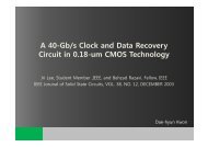
1.25/2.5-Gb/s Dual Bit-Rate Burst-Mode Clock<br />
Recovery Circuit Using Gated-Oscillators<br />
Pyung-Su Han<br />
Dept. of Electrical and Electronic Engineering<br />
Yonsei University<br />
Seoul, Korea<br />
ps@tera.yonsei.ac.kr<br />
Woo-Young Choi<br />
Dept. of Electrical and Electronic Engineering<br />
Yonsei University<br />
Seoul, Korea<br />
wchoi@yonsei.ac.kr<br />
Abstract - A burst-mode clock recovery circuit with a<br />
novel dual-mode structure is presented. It utilizes two<br />
gated-oscillators to align recovered clock edges to data. It<br />
can operate in double data-rate mode in which both rising<br />
and falling edges of recovered clock are used. To enable<br />
this, gated-oscillator reset-phase control scheme is<br />
introduced to switch the starting phase of gated-oscillator<br />
dynamically between 0° and 180° according to current<br />
clock phase. A prototype chip was designed with 0.18µm<br />
CMOS technology, whose 1.25/2.5-Gb/s dual-mode clock<br />
recovery operation is successfully verified by SPICE<br />
simulation.<br />
Keywords: Burst mode, Clock recovery, Gated oscillator,<br />
Multi bit-rate.<br />
1. Introduction<br />
In burst-mode transmission systems, fast clockacquisition<br />
is very important so that preamble bit sequence<br />
can be minimized and transmission throughput maximized.<br />
Various circuit techniques and clock recovery schemes [1]<br />
[2] have been proposed for achieving it. Among them,<br />
gated-oscillator approach [1] provides simplest structure<br />
with instantaneous locking characteristics. It is especially<br />
attractive for such burst-mode applications as LAN (Local<br />
Area Network) and PON (Passive Optical Network) in<br />
which jitter accumulation is not a major problem [3] since<br />
they are used for short-distance transmission and,<br />
consequently, do not require repeaters. All-pass<br />
characteristics of gated-oscillator-based clock recovery<br />
scheme allow tracking of jitters of all frequency, resulting in<br />
decent jitter tolerance up to very high frequency. [4].<br />
Frequency mismatch between gated-oscillators limits<br />
maximum run-length of CID (Consecutive Identical Digit)<br />
that clock recovery circuit can process. Typically, frequency<br />
mismatches around two or three percent of operation<br />
frequency [5] are observed in standard CMOS technology.<br />
This problem can be relieved by using run-length limiting<br />
coding scheme such as 8b10b code which offers maximum<br />
CID run-length of 5bits [4].<br />
Recently published gigabit rate PON standards (GPON<br />
and EPON) [6] [7] support 1.25-Gb/s per burst-mode<br />
transmission and it is expected to be doubled to 2.5-Gb/s in<br />
near future. Therefore, dual bit-rate clock recovery circuit<br />
that can support both 1.25-and 2.5-Gb/s can be very useful.<br />
In this paper, we presented a novel burst-mode clock<br />
recovery circuit which can operate in half-rate clocking<br />
mode, doubling its operation speed, as well as in<br />
conventional full-rate clock extraction mode.<br />
2. Gated-oscillator based clock recovery<br />
Gated-oscillator based clock recovery scheme was<br />
originally published in 1954 for clock generation of<br />
magnetic drum data storage [8]. After that, PLL (Phase-<br />
Locked Loop) and SAW (Surface Acoustic Wave) filter<br />
based clock recovery schemes, which can offer good jitter<br />
suppression, became dominant among long-haul, high-speed<br />
data transmission applications. Nowadays, however, it is<br />
used in burst-mode systems and in multi-channel receivers<br />
in which many receivers should be integrated on a single<br />
chip [9], because it can provide small-size and low-power<br />
consuming clock recovery circuits.<br />
Fig. 1 shows schematic diagram of a gated-oscillator. A<br />
logic ‘gate’ is inserted in a ring oscillator to turn on and off<br />
its oscillation. When the gate is closed, or ‘Enable’ is low,<br />
the clock edge circulating in the ring oscillator is blocked by<br />
the gate stage and the oscillation stops.<br />
The gated-oscillator in Fig. 1 has only one stable state<br />
when ‘Enable’ is low, that is with high ‘Out’. In this state,<br />
the oscillator is ready to be triggered. By setting ‘Enable’ to<br />
high, the oscillation can be resumed. An important<br />
observation here is that the oscillation is always triggered<br />
off with ‘Out’ signal going to low. That means we can set<br />
the output clock phase to a certain value, in this case, falling<br />
edge, whenever we want to do so by controlling ‘Enable’<br />
signal.<br />
Gated-oscillator based clock recovery utilizes this<br />
property to align clock signal to data bits. Fig. 2 depicts a<br />
gated-oscillator based clock recovery circuit example.<br />
251
Figure 1. Schematic diagram of a gated oscillator<br />
Figure 2. Gated-oscillator based clock recovery circuit<br />
Two gated-oscillators are turned on and off alternately<br />
according to ‘Burst data’ to generate clock signal<br />
synchronized to data. They are tuned to the data rate clock<br />
frequency by sharing the VCO (Voltage Controlled<br />
Oscillator) control voltage of reference PLL which is locked<br />
at reference clock frequency. When ‘Burst data’ is high<br />
(logical one), the lower gated-oscillator is activated and<br />
generates clock, and when ‘Burst data’ is low (logical zero)<br />
and the upper one is activated and generates clock.<br />
Therefore each gated-oscillator covers half portions of<br />
‘Burst data’. Two half portions of clock are combined by an<br />
OR gate to generate complete clock signal. This operation is<br />
shown in Fig. 3.<br />
3. Half-rate clock recovery<br />
Half-rate clocking or DDR (Double Data Rate) scheme<br />
became very popular recently, especially for high-speed<br />
memory I/Os. It uses both rising and falling edges of clock<br />
signal to relieve device speed requirements.<br />
As described in section II, gated-oscillator based clock<br />
recovery scheme utilizes clock-phase-reset-ability of gatedoscillator.<br />
Let us assume that the gated-oscillator clock<br />
recovery circuit shown in Fig. 2 has clock phase set to 180°,<br />
or rising edge, at every data transition. Then the opposite<br />
clock phase (0°), or falling edge can be used for data<br />
sampling.<br />
In half-rate clock recovery, since both rising and falling<br />
edges are used, it should be possible to set gated-oscillator<br />
phase to 180° (rising edge) or 0° (falling edge) according to<br />
the clock phase. In our design, a modified version of gatedoscillator<br />
as shown in Fig. 4 is used to enable half-rate clock<br />
operation.<br />
Gated-oscillator in Fig. 4 uses two MUXs for its gate<br />
stages (their selection signal, used as ‘Enable’, is not shown<br />
in the figure). It has four stable states when deactivated, in<br />
contrast to the conventional one having only one.<br />
Combination of R0 and R1 can select one among them. The<br />
logic values of the output terminal of the gate stages are<br />
arranged by R0 and R1 during stable states. Therefore R0<br />
and R1, called ‘reset value’, can select the starting phase of<br />
gated-oscillator because they are indeed the very output<br />
value O0 and O1 would have just before the oscillation<br />
starts.<br />
Because the clock edges are to be aligned to data<br />
transition, delayed version of clock signal (O0d) should be<br />
used for data sampling in half-rate mode. After clock MUX<br />
(explained later), the total amount of delay of extracted<br />
clock is exactly a quarter of clock period (a half of bit<br />
period), giving the optimal chance for data sampling.<br />
Fig. 5 shows clock phase definition used in this design<br />
and four possible reset phase. For example, if we make both<br />
R0 and R1 high (logical one), the gated-oscillator makes its<br />
output start at 0°. If we use low (logical zero) for R0 and R1,<br />
the oscillation will start at 180°.<br />
A half-rate clock recovery circuit was built with the<br />
modified gated-oscillator and is depicted in Fig. 6. R a and R b ,<br />
should be changed dynamically to make sure the gatedoscillator<br />
to oscillate half-rate frequency. This problem can<br />
be solved by using the activated one’s output clock, O0, as<br />
‘reset value’ of the other. This make the clock phase of<br />
oscillator can set its clock phase to 0° or 180° properly.<br />
Figure 4. Modified gated-oscillator for half-clock recovery<br />
Figure 3. Clock recovery operation using<br />
a gated-oscillator pair<br />
Figure 5. Clock phase definition<br />
252
Fig. 8 shows 2.5-Gb/s input bit stream, recovered halfrate<br />
clock signal, data sampled at rising edges and falling<br />
edges when it operates in half-rate clocking mode.<br />
Figure 6. Half-rate clock recovery circuit<br />
Half portions of clock signals are combined by clock<br />
MUX, instead of OR gate. OR gate cannot be used for clock<br />
combining in half-rate mode, because although when a<br />
gated-oscillator is deactivated, it would make some fake<br />
clock due to continuously changing reset value. This fake<br />
clock is screened out by the clock MUX. But in<br />
functionality, an OR gate and a MUX play the exactly same<br />
role.<br />
Figure 7. Input data, recovered clock and retimed data<br />
waveforms from 1.25-Gb/s full-rate clock recovery<br />
simulation<br />
4. Dual bit-rate operation<br />
Modified gated-oscillator in Fig. 4 also can be used for<br />
full-rate clock recovery by fixing reset value to a constant<br />
logic value, e.g. logical high. Then it operates the same as<br />
the conventional one shown in Fig. 1, although it can settle<br />
faster owing to the additional gate stage (two MUXs) when<br />
the ‘Enable’ turns off the oscillation.<br />
By utilizing this programmability of reset phase, the<br />
clock recovery circuit shown in Fig. 6 can be used for fullrate<br />
clock recovery as well as half-rate clock recovery. In<br />
circuit design, it was implemented by adding two MUXs<br />
with a constant value on their one input (not shown in Fig.<br />
6) in reset value path. They are controlled by external modeselection<br />
signal.<br />
5. Simulation result<br />
Clock recovery circuits described so far and a replica<br />
PLL for frequency tuning were designed with 0.18µm<br />
CMOS technology, and its functionality was verified by<br />
SPICE simulation.<br />
Fig. 7 shows 1.25-Gb/s input bit stream, recovered clock<br />
signal and retimed data bits when it operates in full-rate<br />
clock recovery mode. MATLAB-generated random bit<br />
sequence was used for data input.<br />
Figure 8. Input data, recovered clock and retimed data<br />
waveforms from 2.5-Gb/s full-rate clock recovery<br />
simulation<br />
PWD in recovered clock waveform after several CIDs<br />
was observed. It was caused by clock phase drift due to<br />
frequency mismatch between clock-recovering gatedoscillators<br />
and replica oscillator in PLL and would result in<br />
deterministic jitter. 0.18UI and 0.21UI of peak-to-peak<br />
deterministic jitter were estimated for each of 1.25-Gb/s and<br />
2.5-Gb/s operation by the simulation results, when<br />
maximum run-length of CID was 5bits. Data bits were<br />
correctly retimed because enough timing margin for datasampling<br />
is secured even with this amount of jitter.<br />
6. Prototype chip and measurement result<br />
Fig. 9 is microscopic photograph of fabricated prototype<br />
chip. Clock recovery core occupies only 160µm x 250µm<br />
and replica PLL requires 310µm x 250µm.<br />
253
Figure 9. Layout of the the prototype chip<br />
Figure 12. Instantaneous phase alignment<br />
7. Conclusions<br />
A novel structure of burst-mode clock recovery circuit<br />
was proposed. It can operate in half-rate clock frequency<br />
mode, which doubles the operation speed, as well as fullrate<br />
clock recovery. The two operation modes can be<br />
switched simply by external selection signal. Proposed<br />
circuit was designed with 0.18µm CMOS technology and<br />
prototype chip was fabricated.<br />
Figure 10. Recovered clock from 1.25Gbps 2 7 -1 PRBS<br />
Some PWD was observed in simulation, which was<br />
caused by clock phase drift due to frequency offset between<br />
oscillators in clock recovery circuit and replica PLL. This<br />
problem can be mitigated by using limited-CID coding<br />
scheme, e.g., 8b10b code that limits maximum run-length of<br />
CID to 5bits. In prototype measurement, PRBS 2 7 -1 pattern<br />
was used which has maximum run length of 7bit. Prototype<br />
chip successfully recovered full-rate and half-rate clock<br />
from each 1.25Gbps and 2.5Gbps PRBS patterns.<br />
Table 1 sums up the measurement result.<br />
Table 1. Measurement result summary<br />
Figure 11. Recovered clock from 2.5Gbps 2 7 -1 PRBS<br />
Figure 10 and 11 show recovered clock waveforms from<br />
2 7 -1 PRBS pattern at 1.25Gbps/2.5Gbps each. Because data<br />
source is virtually free from jitter, observed peak-to-peak<br />
jitter of around 100ps was purely from clock recovery<br />
circuit itself.<br />
Figure 12 shows burst-mode operation of prototype chip.<br />
Intentional phase drift were made by substitution of PRBS<br />
patterns by 55bits of 0’s. Instantaneous phase alignment<br />
operation was observed at the end of stuffed 0’s where<br />
following data transition occurred.<br />
Technology 0.18µm CMOS<br />
Data-rate<br />
1.25Gbps/2.5Gbps (dual bit-rate)<br />
Chip area<br />
160µm x 250µm for core<br />
310µm x 250µm for reference PLL<br />
Max. run-length More than 7bits<br />
Jitter generation 100ps p2p for 1.25Gbps/2.5Gbps<br />
Power supply 1.8V<br />
Power consumption<br />
60mW for core<br />
50mW for Output buffer<br />
Acknowledgement<br />
This work was sponsored by the Ministry of Science and<br />
Technology of Korea and the Ministry of Commerce,<br />
Industry and Energy through the System IC 2010 program.<br />
We also acknowledge that EDA software used in this work<br />
was supported by IDEC(IC <strong>Design</strong> Education Center).<br />
254
The authors are grateful to Jin-Up Lim, Chang-Kyung Sung,<br />
and Jae-Kwan Kwon for their assistance in prototype chip<br />
layout. They are also thankful to Jae-Wook Lee and Do-ho<br />
Kim for their helpful discussions.<br />
References<br />
[1] M. Banu and A. E. Dunlop, “Clock recovery circuit<br />
with instantaneous locking”, Electronic letters, Vol. 28, No.<br />
23, pp.2127 – 2130, 1992<br />
[2] Chih–Kong Ken Yang and Mark A. Horowitz, “A 0.8-<br />
µm CMOS 2.5Gb/s oversampling receiver and transmitter<br />
for serial links”, IEEE J. Solid-State Circuits, Vol. 31, No.<br />
12, pp. 2015 – 2023, December 1996<br />
[3] Kishine, K., Ishihara, N., Takiguchi, K., Ichino, H., “A<br />
2.5-Gb/s clock and data recovery IC with tunable jitter<br />
characteristics for use in LAN’s and WAN’s”, IEEE J.<br />
Solid-State Circuits, Vol. 34, No. 6, pp. 805 – 812, June<br />
1999<br />
[4] Shunichi Kaeriyama, Masayuki Mizuno, “A 10Gb/s/ch<br />
50mW 120x130µm 2 clock and data recovery circuit”,<br />
Internaltional Solid-State Circuits <strong>Conference</strong>, 2003.,<br />
Digest of Technical Papers, Page(s):70 - 478 vol.1<br />
[5] Do-ho Kim, Pyung-Su Han, and Woo-Young Choi,<br />
“1.25Gb/s burst-mode CDR with robustness to duty cycle<br />
distortion”, SOC conference <strong>2005</strong><br />
[6] “G.984-2 Gigabit-capable passive optical networks<br />
(GPON): Physical media dependent (PMD) layer<br />
sepcification”, ITU-T, 2003<br />
[7] “IEEE 802.3ah amendment: media access control<br />
parameters, physical layers, and management parameters<br />
for subscriber access networks”, IEEE Computer Society,<br />
2004<br />
[8] L. D. Seader, “A self-clocking system for information<br />
transfer”, IBM Journal, pp. 181 – 184, April 1957<br />
[9] Muller, P. Tajalli, A. Atarodi, M. Leblebici, Y., “Topdown<br />
design of a low-power multi-channel 2.5-<br />
Gbit/s/channel gated oscillator clock-recovery circuit”,<br />
<strong>Design</strong>, Automation and Test in Europe, <strong>2005</strong>. Proceedings<br />
7-11 March <strong>2005</strong> Page(s):258 - 263 Vol. 1<br />
255