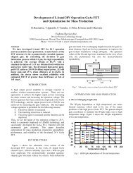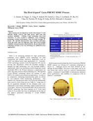
Large Diameter M-HEMT & InP-HEMT Epiwafers ... - CS Mantech
Large Diameter M-HEMT & InP-HEMT Epiwafers ... - CS Mantech
Large Diameter M-HEMT & InP-HEMT Epiwafers ... - CS Mantech

You also want an ePaper? Increase the reach of your titles
YUMPU automatically turns print PDFs into web optimized ePapers that Google loves.
Copyright © 2001, GaAs MANTECH, Inc.<br />
<strong>Large</strong> <strong>Diameter</strong> M-<strong>HEMT</strong> & <strong>InP</strong>-<strong>HEMT</strong> <strong>Epiwafers</strong> Grown<br />
in Multicharge MOVPE Reactors<br />
*Takeshi Tanaka, Tatsushi Hashimoto, Mineo Washima and **Yohei Otoki<br />
Advanced Research Center (ARC), Hitachi Cable, Ltd., 3550 Kidamari, Tsuchiura, Ibaraki, 300-0026 Japan<br />
phone: +81-298-26-7655, fax: +81-298-26-6411, email: ttanaka@arc.hitachi-cable.co.jp<br />
Abstract<br />
<strong>Large</strong> diameter M-<strong>HEMT</strong> and <strong>InP</strong>-<strong>HEMT</strong> epitaxial<br />
wafers were fabricated in a lately installed Hitachi Cable’s<br />
MOVPE reactor that was outfitted with mass production<br />
capability (8x4" or 5x6"). M-<strong>HEMT</strong> structure was combined<br />
with In 0.15 Ga 0.85 P layer, which had the same lattice constant<br />
with In 0.36 Ga 0.64 As channel and could be used for etch stop<br />
and/or surface passivation. Both of the M-<strong>HEMT</strong> and<br />
<strong>InP</strong>-<strong>HEMT</strong> wafers showed reasonable performance with<br />
abrupt etching selectivity, which will simplify device<br />
fabrication processed and realize high yield rates. Excellent<br />
uniformity overall the substrates was also achieved by<br />
optimizing atmospheres inside the reactor. These wafers will<br />
satisfactorymeetthedemandsinthenextgenerationlownoise<br />
and high power RF devices for wireless application and<br />
opto-electronic communication markets.<br />
INTRODUCTION<br />
The expansion of cellular phone market and upcoming<br />
demands in millimeter-wave range operations in wireless-LAN,<br />
LMDS and ITS have stimulated the recent development of<br />
M(Metamorphic)-<strong>HEMT</strong>, which has the right characteristics<br />
for low noise and high power amplification at high frequency.<br />
Meanwhile, “wired” fiber-related components, in which<br />
40Gbit/sec optic communication will be started in 2001, needs<br />
digital and analog integrated circuit with high maximum<br />
oscillation frequency. <strong>InP</strong>-<strong>HEMT</strong> and M-<strong>HEMT</strong>, which have<br />
high electron mobility and enough transport characteristics, are<br />
also indispensable devices for these high-speed ICs. Thus there<br />
is an impending need of large diameter epiwafers of M-<strong>HEMT</strong><br />
and <strong>InP</strong>-<strong>HEMT</strong>, especially wafers grown by MOVPE<br />
(Metal Organic Vapor Phase Epitaxy), which has some<br />
advantages over the other epitaxial systems from the<br />
viewpoint of commercial application. At last year’s<br />
MANTECH conference, we made the first report on the<br />
feasibility of M-<strong>HEMT</strong> wafers using MOVPE method [1].<br />
Our client’s requests motivate us to transfer this laboratory<br />
level experimental technique into mass production<br />
technology. In this report, we will show successful development<br />
in large diameter M-<strong>HEMT</strong> wafer growth using Hitachi-Cable’s<br />
lately installed multi charge MOVPE reactor. The possibility<br />
of InGaP layer growth, which lattice matches to M-<strong>HEMT</strong><br />
channel and will be used as etch stopper, is also explained. In<br />
addition, our capability of fabricating high uniformity<br />
<strong>InP</strong>-<strong>HEMT</strong> epiwafer, which is the precede alternative of<br />
M-<strong>HEMT</strong>, will be shown.<br />
MANUFACTURING EQUIPMENT<br />
We installed a new MOVPE system which had been<br />
designed to minimize the total epigrowth time and increase the<br />
number of holding wafers while maintaining clean surfaces, a<br />
contamination free epi/substrate interface, high doping<br />
efficiency, excellent uniformity and reproducibility reported<br />
before [2]. The planetary configuration and the face down system<br />
were combined to improve throughput and realize these quality<br />
(Fig.1). The wafers, five 6” or eight 4”, are loaded automatically<br />
from cassette to the reactor and set in a face down style. Gas then<br />
flows from the center of the bottom plate of the reactor. Both<br />
the susceptor (wafer holder) and the individual wafer rotate<br />
during the growth to achieve inside-wafer and wafer-to-wafer<br />
uniformity. The heating and cooling time are much reduced<br />
compared to that of the conv entional horizontal-flow type reactor<br />
Heater<br />
Susceptor<br />
Current address<br />
* Microelectronics Lab., ECE, University of Illinois at U-C, 208<br />
N. Wright St., Rm.319A, Urbana, IL 61801<br />
email: ttanaka@hsic.micro.uiuc.edu<br />
** Hitaka Works, Hitachi Cable, Ltd., 880 Isagozawa-cho,<br />
Hitachi, Ibaraki, 319-1418 Japan<br />
email: otoki.yohei@hitachi-cable.co.jp<br />
Wafers<br />
Gas<br />
Fig. 1 System configuration of planetary and face-down MOVPE<br />
reactor used in this study. It was designed to rotate both the susceptor<br />
(wafer holder) and the individual wafer during the growth in order to<br />
improve uniformity.
n + -In 0.36 Ga 0.64 As<br />
i-In 0.85 Ga 0.15 P<br />
i-In 0.35 Al 0.65 As<br />
n-In 0.35 Al 0.65 As<br />
due to the small thermal mass of the new reactor. These<br />
improvements in mass production reactors allow us to increase<br />
through put for most of our products, including the M-<strong>HEMT</strong><br />
wafers.<br />
SAMPLE PREPARATION<br />
contact<br />
etch stop<br />
shottky<br />
supply<br />
(10 nm)<br />
(11 nm)<br />
(9 nm)<br />
i-In 0.35 Al 0.65 As spacer (6 nm)<br />
i-In 0.36 Ga 0.64 As channel (30 nm)<br />
i-In x Al 1-x As<br />
step-graded buffer<br />
S.I. GaAs(100) substrate<br />
Fig. 2 Cross section of the structure of M-<strong>HEMT</strong><br />
epiwafer used in this study.<br />
All the samples were grown in MOVPE system mentioned<br />
above. Atmosphere in the reactor is low pressure (50 Torr)<br />
Hydrogen. Trimethylindium (TMI), trimethylaluminum<br />
(TMA) and trimethylgallium (TMG) were used as group III<br />
elements precursors, and both of arsine (AsH 3 ) and phosphine<br />
(PH 3 ) gases were chosen as group V sources. n-type doping is<br />
achieved by selenium, using H 2 Se as a precursor. We need<br />
relatively high substrate temperature up to 700°C, in order to<br />
prevent impurity contamination into the InAlAs layer and<br />
accomplish superior morphology of the surfaces of epiwafers.<br />
Carrier gas flow rate and susceptor heater balance were optimized<br />
to achieve uniformity of indium composition in the epilayers.<br />
Figure 2 shows the cross sectional view of one of the M-<strong>HEMT</strong><br />
epi structures grown on S.I. GaAs (100) substrate. The indium<br />
composition in each layer was determined by using 4-crystal<br />
XRD. Step-graded InAlAs buffer layers effectively decrease<br />
misfit dislocations and In (x) Ga (1-x) As (indium mole fraction<br />
x=35-40%) channel layer will show high mobility, high sheet<br />
electron concentration and relatively high on-state breakdown<br />
voltages. In addition, an In (y) Ga (1-y) P (indium mole fraction<br />
y=85-90%) etch-stop and passivation layer was inserted upon<br />
the InAlAs shottky layer. The phosphide layer has high etching<br />
selectivity, which can make device process more simple, improve<br />
Vp uniformity and realize high yield rates. It is also expected<br />
that phosphide surface passivation layer leads to better noise<br />
figure and long-term reliability. In order to evaluate the ability<br />
to etch-stop, we grew an wafer with n-In 0.36 Ga 0.64 As(200nm)/<br />
i-In 0.85 Ga 0.15 P(10nm)/ n-In 0.36 Ga 0.64 As(200nm) epistructure.<br />
This sample was etched by H 3 PO 4 :H 2 O 2 :DI water=1:1:10<br />
solution and the change of sheet carrier concentration in this<br />
sample along with the etching time was plotted to calculated<br />
the etch rate and etching selectivity between the arsenide and<br />
phosphide layers. <strong>InP</strong>-<strong>HEMT</strong>, which also has InAlAs<br />
buffer/shottky and InGaAs channel layers, although the indium<br />
composition is higher (53%) than M-<strong>HEMT</strong>, was also grown<br />
on 4” semi-insulating M/A-COM <strong>InP</strong>(100) substrate, using the<br />
same growth condition with our M-<strong>HEMT</strong>. Electron mobility<br />
in both of M-<strong>HEMT</strong> and <strong>InP</strong>-<strong>HEMT</strong> were characterized by Van<br />
der Pauw measurement at room temperature.<br />
RESULTS AND DISCUSSION<br />
The dispersion of electron mobility in the 4-inch M-<strong>HEMT</strong><br />
epiwafers are plotted in figure 3. The mobility in conventional<br />
P-<strong>HEMT</strong> was also added in the figure for comparison. M-<strong>HEMT</strong><br />
wafer showed 8,000 cm 2 /Vs mobility at 2.5x10 12 cm -2 sheet<br />
carrier concentration, which was about 30% overtaking the<br />
mobility in P-<strong>HEMT</strong> epiwafer. The higher indium composition<br />
in InGaAs channel layer grown on step-graded InAlAs buffer<br />
layer in metamorphic epi structure realized this high electron<br />
transportation characteristic. Variation of the mobility in<br />
M-<strong>HEMT</strong> was 1.48%, meaning that high electron mobility was<br />
uniformly achieved overall 4-inch GaAs substrate. The mobility<br />
in <strong>InP</strong>-<strong>HEMT</strong> was also shown in figure 3. The value reached<br />
to 12,000 cm 2 /Vs at room temperature and its diagonal<br />
uniformity was also sufficient.<br />
Figure 4 shows the result of etch-stop characterization.<br />
In 0.36 Ga 0.64 As layer was etch during the first 30 second at etch<br />
rate of 6.7 nm/sec, and then InGaP layer appeared to surface,<br />
where etch rate was reduced to 0.167nm/sec. It is understood<br />
that etch speed was abruptly changed at the InGaAs/InGaP<br />
interface and enough etching selectivity was obtained. The<br />
growth of phosphide layers with abrupt interfaces is one of our<br />
Electron mobility (cm 2 /Vs)<br />
14,000<br />
12,000<br />
10,000<br />
8,000<br />
6,000<br />
4,000<br />
2,000<br />
0<br />
In 0.53 GaAs channel <strong>InP</strong>-<strong>HEMT</strong><br />
In 0.36 GaAs channel M-<strong>HEMT</strong><br />
In 0.20 GaAs channel<br />
Conventional P-<strong>HEMT</strong><br />
-50 -25 0 25 50<br />
Diagonal position (mm)<br />
Fig. 3 Electron mobility in In 0.36 Ga 0.64 As channle M-<strong>HEMT</strong> and<br />
In 0.53 Ga 0.47 As channel <strong>InP</strong>-<strong>HEMT</strong> epiwafers grown by MOVPE.<br />
Both of them were grown on 4 inch substrates. Mobility in<br />
conventional P-<strong>HEMT</strong> was also shown for comparison.
Depth (nm)<br />
500<br />
400<br />
300<br />
200<br />
100<br />
0<br />
Etch stop time<br />
0 20 40 60 80 100 120<br />
Etch time (sec)<br />
Fig. 4 Etching depth as a function of etch time. n-In 0.36 Ga 0.64 As(200nm)/<br />
i-In 0.85 Ga 0.15 P (10nm)/n-In 0.36 Ga 0.64 As (200nm) etch-stop test structure<br />
grown on metamorphic buffer layer was etched by H 3 PO 4 :H 2 O 2 :H 2 O =<br />
1:1:10 solution to evaluate the etching selectivity between InGaAs and<br />
InGaP.<br />
greatest assets with MOVPE, compared with solid source MBE<br />
that has difficulty in phosphide epi growth.<br />
CONCLUSIONS<br />
We are now ready to supply M-<strong>HEMT</strong> epiwafer with InGaP<br />
etch-stop & passivation layer and <strong>InP</strong>-<strong>HEMT</strong> epiwafer by using<br />
our new multicharge high throughput MOVPE reactor in mass<br />
production line. Both of 4 inch M-<strong>HEMT</strong> and <strong>InP</strong>-<strong>HEMT</strong> wafers<br />
showed reasonable electric characteristics and excellent<br />
uniformity. These waferes will satisfactory meet the demands<br />
in the next generation low noise and power RF devices for wireless<br />
application markets.<br />
REFERENCES<br />
[1] T. Tanaka, et al., Digest of MANTEC ‘00, Washington D.<br />
C., (2000) p.89<br />
[2] Y.Otoki et.al., Digest of MANTECH 98, Seattle,(1998) p.137