40nm...40 Nanometer - UMC
40nm...40 Nanometer - UMC
40nm...40 Nanometer - UMC

You also want an ePaper? Increase the reach of your titles
YUMPU automatically turns print PDFs into web optimized ePapers that Google loves.
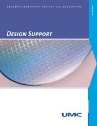
F O U N D R Y L E A D E R S H I P F O R T H E S o C G E N E R A T I O N<br />
40 <strong>Nanometer</strong><br />
40<br />
www.umc.com
40 <strong>Nanometer</strong> - Customer-Driven Foundry Solutions<br />
<strong>UMC</strong>’s volume production 40-nanometer technology supports today’s high performance and low power requirements. Many customers<br />
have engaged with <strong>UMC</strong> for their <strong>40nm</strong> projects, with multiple designs in various stages of production. <strong>UMC</strong>'s <strong>40nm</strong> utilizes advanced<br />
processes such as immersion lithography, ultra shallow junction, mobility enhancement techniques and ultra low-k dielectrics for<br />
maximum power and performance optimization. <strong>UMC</strong>'s <strong>40nm</strong> process consists of a low power platform (LP) focusing on the low<br />
power and low leakage design requirements for mobile and consumer applications, and a generic platform (G) that is optimized for<br />
a broad range of consumer and high-speed applications. Designers also benefit from comprehensive device offerings that include<br />
features to help optimize power and performance, different I/O voltage choices and analog/RF design resources.<br />
<strong>40nm</strong> Key Features<br />
• Integrated flows for logic, Mixed-Signal/RF<br />
• Shallow trench isolation<br />
• Advanced mobility enhancement<br />
techniques (Channel orientation, SMT, DSL,<br />
eSiGe)<br />
• Retrograde twin well (Triple well option)<br />
Prtbe . Wires. Consumer• Wirless<br />
• Immersion Lithography implemented by<br />
NA=1.2<br />
• Up to 1P11M copper metal layers with ULK<br />
(k=2.5)<br />
• 6T/8T SRAM bit cell option<br />
• Mini-second anneal Portable technology . Wireless for ultra . Consumer • e-Fuse option<br />
shallow junction<br />
Portable . Wireless . Consumer • BOAC (Bonding Over Active Circuit)<br />
• Poly gate & S/D with NiSi process<br />
• Wire Bond/Flip Chip option<br />
Technology to Meet Broad Applications<br />
<strong>UMC</strong> <strong>40nm</strong> Technology<br />
Low Power (LP)<br />
Generic (G)<br />
Portable • Wireless • Consumer<br />
Graphics • Network
<strong>40nm</strong> Logic/MS/RF Devices<br />
<strong>40nm</strong> Logic/MS/RF Technology<br />
Core Devices<br />
I/O Devices<br />
MS/RF Devices<br />
G_LVt 0.9V(1.0V)<br />
1.8V I/O<br />
Native Vt<br />
G_RVt 0.9V(1.0V)<br />
2.5V I/O (OD 3.3V;UD 1.8V)<br />
Bipolar<br />
G_HVt 0.9V(1.0V)<br />
Diodes<br />
LP_uLVt 1.1V<br />
MIM/MOM<br />
LP_LVt 1.1V<br />
NCAP<br />
LP_RVt 1.1V<br />
Resistors<br />
LP_HVt 1.1V<br />
Inductor<br />
G: Generic Platform LP: Low Power : RF model available; other models available upon customer request<br />
Comprehensive IP Portfolio<br />
<strong>UMC</strong> offers comprehensive design<br />
resources that enable our customers<br />
to fully realize the advantages of<br />
<strong>UMC</strong>'s advanced technologies. <strong>UMC</strong>'s<br />
fundamental IPs (standard cells, I/Os,<br />
and memory compilers) help customers<br />
easily migrate their designs to the next<br />
process generation to realize significant<br />
performance advantages while also<br />
reducing die size. Customers can also<br />
leverage application specific IPs that are<br />
specialized for all types of mainstream<br />
applications such as digital TVs, cellular<br />
baseband controllers, graphics, and<br />
networking to overcome time-to-market<br />
challenges.<br />
DTV<br />
PLL, USB, LVDS,<br />
Embedded Memory,<br />
HDMI, DDRn<br />
Graphic<br />
DDRn, PCI-e,<br />
HDMI, LVDS,<br />
Embedded Memory<br />
Baseband<br />
Mobile DDR,USB,<br />
LVDS, PLL,<br />
Embedded Memory<br />
Networking<br />
Mobile DDR, USB,<br />
PCI-e, SATA,<br />
Embedded Memory
Fundamental IP Support<br />
Fundamental IPs (standard cells, I/Os, and memory compilers listed below) are optimized to <strong>UMC</strong> technologies, and are planned<br />
for development from several leading vendors to be available free-of-charge (please contact a <strong>UMC</strong> account manager for more<br />
information). Customers can also leverage application specific IPs for DTV, graphics, networking, etc. IPs available through <strong>UMC</strong> are<br />
DFM (Design for Manufacturing) compliant for better manufacturability.<br />
Process Node<br />
G<br />
<strong>40nm</strong><br />
LP<br />
Ultra-LVT - Þ<br />
Standard Cell Library<br />
LVT Þ Þ<br />
RVT Þ Þ<br />
HVT Þ Þ<br />
I/O Library 2.5V *(2) Þ Þ<br />
Single Port SRAM Compiler Þ Þ<br />
Dual Port SRAM Compiler Þ Þ<br />
Single Port Register File Þ Þ<br />
Dual Port Register File Þ Þ<br />
ROM Compiler Þ Þ<br />
*(1) The listed IPs are planned for <strong>40nm</strong> development. For the most updated information, please contact your account manager.<br />
*(2) 1.8V/2.5V/3.3V multi-voltage I/O library<br />
Interface/Functional IP Support<br />
ITEM Feature Vandor <strong>40nm</strong> LP<br />
USB 2.0 pico PHY Synopsys Þ<br />
USB 3.0 5Gb/s Synopsys Þ<br />
PCIE Gen II Synopsys Þ<br />
SATA3 6G Synopsys Þ<br />
DDR multi PHY DDR2, 3, 3L, mDDR, LPDDR2 PHY(1066) Synopsys Þ<br />
DDR 3/2 1600MHz Synopsys Þ<br />
HDMI 1.4a TX & HEAC Synopsys Þ<br />
OTP 8Kb~4Mb Kilopass Þ<br />
MIPI D PHY TX & RX Synopsys Þ<br />
PLL<br />
Input frequency range:25~66MHz,<br />
Output frequency range:200~400MHz<br />
FTC<br />
Þ<br />
PLL<br />
Input frequency range:20~200MHz,<br />
Output frequency range:500~ 1000MHz<br />
FTC<br />
Þ<br />
*For more information, please contact your account manager.
Low Power Features of Standard Cell Library<br />
With today's proliferation of low power applications, lowering energy consumption without sacrificing performance has become<br />
a critical concern for designers of power management chips for portable electronics. <strong>UMC</strong> supports its standard cell library with<br />
low power design features, including multiple Vt, clock-gating, level shifter and other features to complement <strong>UMC</strong>’s complete low<br />
power solution.<br />
Operating<br />
Power<br />
Type<br />
Voltage Island<br />
& Scaling<br />
Clock Gating &<br />
Frequency<br />
Scaling<br />
Support Features<br />
Level Shifters<br />
w / Insulator<br />
Power &<br />
Timing Model<br />
@ 80% of Vdd<br />
Support<br />
<strong>40nm</strong> 65nm 90nm 0.13um<br />
Þ Þ Þ Þ<br />
Clock Gated F/F Þ Þ Þ Þ<br />
Multi-Vt Multi-Vt cells Þ Þ Þ Þ<br />
Leakage<br />
Power<br />
Power Gating<br />
Isolation cells, Retention F/F<br />
Headers / Footers, etc.<br />
Þ Þ Þ Þ<br />
Body Bias<br />
Tapless cells<br />
Timing /<br />
Power Model<br />
Þ Þ Þ Þ
Low Power Design Support<br />
Front-end design<br />
Low leakage<br />
process<br />
Power<br />
gating<br />
Multi Vth<br />
Multi VDD<br />
Low power<br />
synthesis<br />
Clock<br />
gating<br />
Voltage and<br />
frequency scaling<br />
Body bias<br />
Back-end design<br />
80%<br />
60% 40% 20% 20% 40% 60% 80%<br />
Leakage Power Saving<br />
Dynamic Power Saving<br />
<strong>UMC</strong> Reference Design Flow<br />
<strong>UMC</strong> Reference Design Flow provides a design<br />
methodology and flow validated with a<br />
“Leon2” system demonstration board. The flow<br />
incorporates 3rd-party EDA vendors’ baseline<br />
design flows to address issues such as timing<br />
closure, signal integrity, leakage power and design<br />
for manufacturability and adopts a hierarchical<br />
design approach built upon silicon validated<br />
process libraries. <strong>UMC</strong> Reference Design Flow<br />
covers from RTL coding all the way to GDS-II<br />
generation and supports Cadence, Magma,<br />
Mentor and Synopsys EDA tools. All of these tools<br />
can be interchanged for added flexibility.<br />
I/O & Memory<br />
Simulation View<br />
Timing View<br />
Timing Constraint &<br />
DFT Requirements<br />
Cell Function, Area,<br />
Timing & Power View<br />
Physical & Noise View<br />
DRC/LVS<br />
Rule Deck<br />
Product Definition/Spec & Tech-dependent Setting<br />
RTL Coding & Simulation<br />
Logic Synthesis<br />
Static Timing Analysis & Gate-level Simulation<br />
Floorplan & Partition<br />
Block & Top Implementation<br />
Physical Verification<br />
Tape-out
Reference Design Flow and Vendor Support<br />
<strong>UMC</strong> works with leading EDA tool companies to provide a verified Reference Design Flow program to ensure the accuracy of customer<br />
designs in a proven environment. <strong>UMC</strong>’s Reference Design Flow program integrates solutions for digital designs and low power<br />
solutions that incorporate the latest DFM resources available from leading third-party providers. Tools can be interchanged for added<br />
flexibility.<br />
Features of Design Flow Cadence Synopsys Magma Mentor<br />
Functional Logic Simulation -<br />
Schematic Entry - - - -<br />
Logic Synthesis -<br />
Static Timing Analysis -<br />
Timing Closure -<br />
Signal Integrity -<br />
Floor Planning -<br />
Physical Synthesis -<br />
Multi-Vt Low Power -<br />
Multi-Vdd Low Power -<br />
Design For Test -<br />
Design For Diagnosis -<br />
DFM - double via insertion<br />
DFM - dummy metal filling<br />
Circuits Simulation<br />
Power Analysis -<br />
Layout Editor - -<br />
Place & Route -<br />
Physical Verification<br />
Formal Verification -<br />
Parasitic Extraction<br />
Noise Analysis -<br />
Note:<br />
Available
DFM Methodology<br />
<strong>UMC</strong> offers optimal DFM (Design For<br />
Manufacturability) solutions to effectively<br />
and efficiently address factors that may<br />
negatively affect yield and performance for<br />
advanced technology designs. <strong>UMC</strong>’s DFM<br />
solutions include advanced process models<br />
incorporated in SPICE and extraction decks<br />
for predicting random and systematic<br />
variations, technology files, DFM-compliant<br />
libraries and IP that embrace the intricacies<br />
of the fabrication process. Concise DFM<br />
recommendation rules are available<br />
along with a comprehensive rule-deck<br />
runset strategy to fulfill various design<br />
requirements.<br />
DFM Methodology Roadmap<br />
Restricted Rules<br />
Statistical Timing Analysis<br />
Critical Area Analysis<br />
Modeling with CMP Effects<br />
Litho Simulation Checks<br />
Modeling with LOD & WPE<br />
Monte Carlo Models<br />
Modeling with WEE<br />
<strong>UMC</strong> also offers pre-tapeout Optical<br />
Proximity Correction (OPC) and Litho Rule DFM Rules<br />
Check (LRC) for custom designs in addition<br />
to our standard post-tapeout services that<br />
include OPC, Litho Simulation Check (LSC),<br />
dummy fill, and metal slotting. At 65nm<br />
and below, <strong>UMC</strong> offers a DFM Design<br />
0.13um 90nm 65nm <strong>40nm</strong><br />
Enablement Kit (DEK) to seamlessly support model-based DFM tools. The DEK has a built-in Graphic User Interface (GUI) for DFM design<br />
database setup, and is completed with application notes and qualification reports for design reference.<br />
<strong>UMC</strong> e-Fuse Features<br />
To reduce chip area, achieve better reliability<br />
performance, and shorten repair time<br />
compared to conventional Al fuse, <strong>UMC</strong><br />
has developed an e-fuse solution to target<br />
the needs of a broad range of applications.<br />
The fuse array and complete functional<br />
macro are offered to ease the integration<br />
process for customers. Both wafer level and<br />
package level fuse are supported. Moreover,<br />
customers can use e-fuse for the OTP (one<br />
time programming) function to save overall<br />
costs.<br />
Logic Compatible<br />
Complete Functional<br />
IP Macros<br />
Design-Friendly Features<br />
Flexibility<br />
• No extra masks necessary<br />
• Only one extra pad required<br />
• Fuse array, programming circuit, sensing amplifier<br />
• Serial and parallel architecture<br />
• Allows metal routing over fuses (M6 and above)<br />
• Programmable at package level<br />
• Wafer level fuse options<br />
• Package level fuse options
Virtual Inductor Library<br />
<strong>UMC</strong> has worked with its EDA tool partners<br />
to deliver the industry's first parameterized<br />
inductor design kit based on full-wave<br />
simulation: the Virtual Inductor Library (VIL).<br />
The VIL enables RFCMOS designers to create<br />
and simulate custom inductor geometries<br />
that are compatible with <strong>UMC</strong>'s processes.<br />
It is built upon <strong>UMC</strong>'s Electromagnetic<br />
Design Methodology (EMDM), which allows<br />
engineers to easily and accurately create<br />
any RF structure. EMDM gives designers<br />
the flexibility to innovate new geometries<br />
simply by editing parameters such as<br />
diameter, number of turns or width.<br />
Spiral<br />
Differential w/o<br />
center tap<br />
Differential with<br />
center tap<br />
The GUI based VIL can be used to simulate all types of RF inductors.<br />
Stack<br />
Virtual Capacitor Library<br />
<strong>UMC</strong> and its EDA tool partners have delivered<br />
the industry's first parameterized MOM<br />
capacitor design kit based on full-wave<br />
simulation: the Virtual Capacitor Library<br />
(VCL). The VCL enables RFCMOS designers<br />
to create and simulate custom capacitor<br />
geometries that are compatible with<br />
<strong>UMC</strong>'s processes. It is built upon <strong>UMC</strong>'s<br />
Electromagnetic Design Methodology<br />
(EMDM), which allows engineers to easily<br />
and accurately create any RF structure.<br />
EMDM gives designers the flexibility to<br />
innovate new geometries simply by editing<br />
parameters such as number of metal and<br />
fingers, arrays, and length of fingers for<br />
capacitor.<br />
The GUI based VCL can be used to simulate all types of RF capacitors.
Virtual Transformer Library<br />
<strong>UMC</strong> has also worked with its EDA tool partners to deliver the industry's first parameterized transformer design kit based on fullwave<br />
simulation: the Virtual Transformer Library (VTL). The VTL enables RFCMOS designers to create and simulate custom transformer<br />
geometries that are compatible with <strong>UMC</strong>'s processes. It is built upon <strong>UMC</strong>'s Electromagnetic Design Methodology (EMDM), which allows<br />
engineers to easily and accurately create any RF structure. EMDM gives designers the flexibility to innovate new geometries simply by<br />
editing parameters such as primary impedance, secondary impedance, number of turns, mode, and frequency for transformer.<br />
Square<br />
Octagon<br />
• Input: single/differential end<br />
• Output: single/differential end<br />
• Turn Ratio: 1:n, n:2n, n:n<br />
The GUI based VTL can be used to simulate all types of RF transformers.<br />
MS/RF Design Flow and<br />
FDK<br />
The FDK (Foundry Design Kit) provides<br />
IC designers with an automatic design<br />
environment. The methodology provides<br />
access to circuit-level design and simulation,<br />
circuit layout, and layout verification with<br />
accurate RF device models. In the front-end,<br />
fundamental components of <strong>UMC</strong>'s MS/<br />
RF process are implemented in common<br />
design environments and simulation tools.<br />
The back-end includes parameterized<br />
cells (P Cell), which include a schematic<br />
driven layout to provide an automatic and<br />
complete design flow. Callback functions are<br />
also provided in the design flow to minimize<br />
data entry. EDA tools for MS/RF designs are<br />
also supported.<br />
Cadence<br />
Schematic (Composer)<br />
(Symbols & CDF)<br />
Schematic<br />
Driven Layout<br />
Circuit Layout<br />
Virtuoso(P-cell)<br />
Verification & Extraction<br />
(DRC/LVS/LPE)<br />
Calibre/XRC<br />
Assura<br />
Tape Out<br />
Virtual Inductor/<br />
Capacitor/Transformer Spec.<br />
Virtual Inductor/<br />
Capacitor/Transformer<br />
Library<br />
Virtual Inductor/<br />
Capacitor/Transformer<br />
Library<br />
Spectre / Spectre RF<br />
Artist<br />
Spectre / Spectre RF<br />
Spectre / Spectre RF<br />
Simulation with Verified<br />
RF/Mixed Signal Models
Optimum Inductor Finder (OIF)<br />
<strong>UMC</strong> offers the Optimum Inductor Finder (OIF) in the FDK package. The OIF gives designers the ability to quickly access a large library<br />
of inductors calibrated to <strong>UMC</strong>'s silicon. It also allows users to perform inductor optimization through just a few simple steps with the<br />
user-friendly interface. For instance, customers can define a desired inductor and make trade-offs between Q-factor and area. The OIF<br />
will select a design that best fits the specifications in a matter of seconds.<br />
Optimum Capacitor Finder (OCF)<br />
<strong>UMC</strong> offers the Optimum Capacitor Finder (OCF) in the FDK package. The OCF gives designers the ability to quickly access a large library<br />
of capacitors calibrated to <strong>UMC</strong>'s silicon. It also allows users to perform capacitor optimization through just a few simple steps with<br />
the user-friendly interface. For instance, customers can define a desired capacitor and make trade-offs between Q-factor and area. The<br />
OCF will select a design that best fits the specifications in a matter of seconds.<br />
Optimum Transformer Finder (OTF)<br />
<strong>UMC</strong> offers the Optimum Transformer Finder (OTF) in the FDK package. The OTF gives designers the ability to quickly access a large library<br />
of transformers calibrated to <strong>UMC</strong>'s silicon. It also allows users to perform transformer optimization through just a few simple steps<br />
with the user-friendly interface. For instance, customers can define a desired transformer and make trade-offs between impedance and<br />
area. The OTF will select a design that best fits the specifications in a matter of seconds.<br />
Analog Design Methodology<br />
FDK EDA Supported Tools<br />
MS/RF<br />
Design Flow<br />
Cadence Mentor ADS Synopsys<br />
Schematic Entry<br />
Composer<br />
ADS<br />
Pre-simulation<br />
Hspice/Spectre<br />
Models<br />
Spectre<br />
SpectreRF<br />
Eldo<br />
EldoRF<br />
ADS<br />
HSPICE<br />
Physical Design<br />
Virtuoso XL<br />
Physical<br />
Verification<br />
(DRC/LVS/RCX)<br />
QRC<br />
Calibre<br />
Calibre XRC<br />
Star RCXT
www.umc.com<br />
F O U N D R Y L E A D E R S H I P F O R T H E S o C G E N E R A T I O N<br />
New Customers<br />
For new customer inquiries,<br />
please direct all questions to<br />
sales@umc.com<br />
Worldwide Contacts<br />
Headquarters:<br />
<strong>UMC</strong><br />
No. 3, Li-Hsin 2nd Road,<br />
Hsinchu Science Park,<br />
Hsinchu, Taiwan, R.O.C.<br />
Tel: 886-3-578-2258<br />
Fax: 886-3-577-9392<br />
Email: foundry@umc.com<br />
In China:<br />
<strong>UMC</strong> Beijing:<br />
Room #521, 5F, South Block,<br />
Raycom InfoTech Park, No.2,<br />
Kexueyuan South Road,<br />
Zhongguancun,<br />
Haidian District,<br />
Beijing 100190, China<br />
Tel: 86-10-59822250<br />
86-18913138053<br />
Fax: 86-10-59822588<br />
HeJian Technology (Suzhou):<br />
No. 333, Xinghua Street, Suzhou<br />
Industrial Park, Suzhou, Jiangsu<br />
Province 215025, China<br />
Tel: 86-512-65931299<br />
Fax: 86-512-62530172<br />
In Japan:<br />
<strong>UMC</strong> Group Japan<br />
15F Akihabara Centerplace Bldg.,<br />
1 Kanda Aioi-Cho Chiyoda-Ku<br />
Tokyo 101-0029 Japan<br />
Tel : 81-3-5294-2701<br />
Fax: 81-3-5294-2707<br />
In Singapore:<br />
<strong>UMC</strong>-SG<br />
No. 3, Pasir Ris Drive 12,<br />
Singapore 519528<br />
Tel: 65-6213-0018<br />
Fax: 65-6213-0005<br />
In Korea:<br />
<strong>UMC</strong> Korea<br />
1117, Hanshin Intervally24, 322,<br />
Teheran-ro, Gangnam-gu,<br />
Seoul, Korea<br />
Tel: 82-2-2183-1790<br />
Fax: 82-2-2183-1794<br />
Email:korea@umc.com<br />
In North America:<br />
<strong>UMC</strong> USA<br />
488 De Guigne Drive,<br />
Sunnyvale, CA 94085, USA<br />
Tel: 1-408-523-7800<br />
Fax: 1-408-733-8090<br />
In Europe:<br />
<strong>UMC</strong> Europe BV<br />
De entree 77<br />
1101 BH Amsterdam Zuidoost<br />
The Netherlands<br />
Tel: 31-(0)20-5640950<br />
Fax: 31-(0)20-6977826<br />
For more information: visit www.umc.com or e-mail sales@umc.com<br />
1402