IEEE Paper Template in A4 (V1) - International Journal of Computer ...
IEEE Paper Template in A4 (V1) - International Journal of Computer ...
IEEE Paper Template in A4 (V1) - International Journal of Computer ...

Create successful ePaper yourself
Turn your PDF publications into a flip-book with our unique Google optimized e-Paper software.
<strong>International</strong> <strong>Journal</strong> <strong>of</strong> <strong>Computer</strong> Applications <strong>in</strong> Eng<strong>in</strong>eer<strong>in</strong>g Sciences<br />
[VOL II, ISSUE III, SEPTEMBER 2012] [ISSN: 2231-4946]<br />
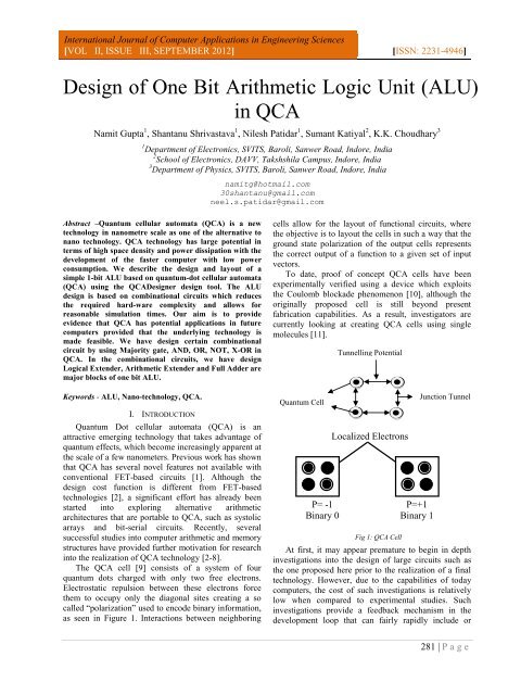
Design <strong>of</strong> One Bit Arithmetic Logic Unit (ALU)<br />
<strong>in</strong> QCA<br />
Namit Gupta 1 , Shantanu Shrivastava 1 , Nilesh Patidar 1 , Sumant Katiyal 2 , K.K. Choudhary 3<br />
1 Department <strong>of</strong> Electronics, SVITS, Baroli, Sanwer Road, Indore, India<br />
2 School <strong>of</strong> Electronics, DAVV, Takshshila Campus, Indore, India<br />
3 Department <strong>of</strong> Physics, SVITS, Baroli, Sanwer Road, Indore, India<br />
namitg@hotmail.com<br />
30shantanu@gmail.com<br />
neel.s.patidar@gmail.com<br />
Abstract –Quantum cellular automata (QCA) is a new<br />
technology <strong>in</strong> nanometre scale as one <strong>of</strong> the alternative to<br />
nano technology. QCA technology has large potential <strong>in</strong><br />
terms <strong>of</strong> high space density and power dissipation with the<br />
development <strong>of</strong> the faster computer with low power<br />
consumption. We describe the design and layout <strong>of</strong> a<br />
simple 1-bit ALU based on quantum-dot cellular automata<br />
(QCA) us<strong>in</strong>g the QCADesigner design tool. The ALU<br />
design is based on comb<strong>in</strong>ational circuits which reduces<br />
the required hard-ware complexity and allows for<br />
reasonable simulation times. Our aim is to provide<br />
evidence that QCA has potential applications <strong>in</strong> future<br />
computers provided that the underly<strong>in</strong>g technology is<br />
made feasible. We have design certa<strong>in</strong> comb<strong>in</strong>ational<br />
circuit by us<strong>in</strong>g Majority gate, AND, OR, NOT, X-OR <strong>in</strong><br />
QCA. In the comb<strong>in</strong>ational circuits, we have design<br />
Logical Extender, Arithmetic Extender and Full Adder are<br />
major blocks <strong>of</strong> one bit ALU.<br />
Keywords - ALU, Nano-technology, QCA.<br />
I. INTRODUCTION<br />
Quantum Dot cellular automata (QCA) is an<br />
attractive emerg<strong>in</strong>g technology that takes advantage <strong>of</strong><br />
quantum effects, which become <strong>in</strong>creas<strong>in</strong>gly apparent at<br />
the scale <strong>of</strong> a few nanometers. Previous work has shown<br />
that QCA has several novel features not available with<br />
conventional FET-based circuits [1]. Although the<br />
design cost function is different from FET-based<br />
technologies [2], a significant effort has already been<br />
started <strong>in</strong>to explor<strong>in</strong>g alternative arithmetic<br />
architectures that are portable to QCA, such as systolic<br />
arrays and bit-serial circuits. Recently, several<br />
successful studies <strong>in</strong>to computer arithmetic and memory<br />
structures have provided further motivation for research<br />
<strong>in</strong>to the realization <strong>of</strong> QCA technology [2-8].<br />
The QCA cell [9] consists <strong>of</strong> a system <strong>of</strong> four<br />
quantum dots charged with only two free electrons.<br />
Electrostatic repulsion between these electrons force<br />
them to occupy only the diagonal sites creat<strong>in</strong>g a so<br />
called “polarization” used to encode b<strong>in</strong>ary <strong>in</strong>formation,<br />
as seen <strong>in</strong> Figure 1. Interactions between neighbor<strong>in</strong>g<br />
cells allow for the layout <strong>of</strong> functional circuits, where<br />
the objective is to layout the cells <strong>in</strong> such a way that the<br />
ground state polarization <strong>of</strong> the output cells represents<br />
the correct output <strong>of</strong> a function to a given set <strong>of</strong> <strong>in</strong>put<br />
vectors.<br />
To date, pro<strong>of</strong> <strong>of</strong> concept QCA cells have been<br />
experimentally verified us<strong>in</strong>g a device which exploits<br />
the Coulomb blockade phenomenon [10], although the<br />
orig<strong>in</strong>ally proposed cell is still beyond present<br />
fabrication capabilities. As a result, <strong>in</strong>vestigators are<br />
currently look<strong>in</strong>g at creat<strong>in</strong>g QCA cells us<strong>in</strong>g s<strong>in</strong>gle<br />
molecules [11].<br />
Quantum Cell<br />
Tunnell<strong>in</strong>g Potential<br />
Localized Electrons<br />
P= -1 P=+1<br />
B<strong>in</strong>ary 0 B<strong>in</strong>ary 1<br />
Fig 1: QCA Cell<br />
Junction Tunnel<br />
At first, it may appear premature to beg<strong>in</strong> <strong>in</strong> depth<br />
<strong>in</strong>vestigations <strong>in</strong>to the design <strong>of</strong> large circuits such as<br />
the one proposed here prior to the realization <strong>of</strong> a f<strong>in</strong>al<br />
technology. However, due to the capabilities <strong>of</strong> today<br />
computers, the cost <strong>of</strong> such <strong>in</strong>vestigations is relatively<br />
low when compared to experimental studies. Such<br />
<strong>in</strong>vestigations provide a feedback mechanism <strong>in</strong> the<br />
development loop that can fairly rapidly <strong>in</strong>clude or<br />
281 | P a g e
Gupta et. al.<br />
exclude new device implementation concepts based on<br />
their potential application <strong>in</strong> these larger circuits. Us<strong>in</strong>g<br />
simulations we have, for example, identified a<br />
fundamental requirement for multilayer capability <strong>in</strong><br />
complex circuits, previously believe unnecessary [12].<br />
The physical <strong>in</strong>teractions between cells may be used<br />
to realize elementary Boolean logic functions. The basic<br />
logic gates <strong>in</strong> QCA are the Majority logic function and<br />
the Inverter which are illustrated <strong>in</strong> Fig. 2. The Majority<br />
logic function can be realized by only 5 QCA cells. The<br />
logic AND function can be implemented from a<br />
Majority logic function by sett<strong>in</strong>g one <strong>in</strong>put<br />
permanently to 0 and the logic OR function can be<br />
Implemented from a Majority logic function by sett<strong>in</strong>g<br />
one <strong>in</strong>put permanently to 1.<br />
Input<br />
Input2<br />
(a) QCA Inverter<br />
(b) QCA Majority Voter<br />
Fig 2: QCA Logic Gates<br />
II. QCA CLOCKING AND DEVICE LEVEL LATCHING<br />
Unlike the transistor, a basic QCA cell has no<br />
<strong>in</strong>herent directionality for <strong>in</strong>formation flow, and a<br />
circuit made <strong>of</strong> un-clocked cells would propagate<br />
<strong>in</strong>formation <strong>in</strong> uncontrollable directions. In order to<br />
control the flow <strong>of</strong> <strong>in</strong>formation <strong>in</strong> a QCA circuit, four<br />
clock signals, each shifted <strong>in</strong> phase by 90o, as shown <strong>in</strong><br />
Figure 3, are used [13,14]. These clock signals are<br />
expected to be generated by a support<strong>in</strong>g technology<br />
such as a CMOS circuit which is used to control the<br />
tunnel<strong>in</strong>g ability <strong>of</strong> electrons with<strong>in</strong> the cell.<br />
Clock Zone 0<br />
Clock Zone 1<br />
Clock Zone 2<br />
Clock Zone 3<br />
1 0<br />
1<br />
0<br />
0<br />
Input1<br />
Input3<br />
Fig 3: QCA Clock<strong>in</strong>g Zones<br />
0<br />
Output<br />
Output<br />
The clock signals act to pump <strong>in</strong>formation <strong>in</strong><br />
controlled directions <strong>in</strong> the circuit as a result <strong>of</strong> the<br />
successive latch<strong>in</strong>g and unlatch<strong>in</strong>g <strong>in</strong> cells connected to<br />
different clock phases. For example, a wire, which is<br />
clocked from left to right with <strong>in</strong>creas<strong>in</strong>g clock<strong>in</strong>g<br />
zones, will carry <strong>in</strong>formation <strong>in</strong> the same direction; i.e.,<br />
from left to right. This acts to pipel<strong>in</strong>e QCA circuits at a<br />
device level. QCA wires allow more than one bit <strong>of</strong><br />
<strong>in</strong>formation to be propagated along the same wire at any<br />
one time. When the clock drops it latches the cells <strong>in</strong>to<br />
one <strong>of</strong> two possible polarizations based on the <strong>in</strong>fluence<br />
<strong>of</strong> all its neighbor<strong>in</strong>g cells. When the clock signal is<br />
high, the cells are relaxed, and have no polarization. The<br />
m<strong>in</strong>imum size <strong>of</strong> the clock<strong>in</strong>g zone is determ<strong>in</strong>ed by the<br />
m<strong>in</strong>imum feature size <strong>of</strong> the technology used to support<br />
clock<strong>in</strong>g. Large clock<strong>in</strong>g zones can be problematic<br />
because signals travel<strong>in</strong>g down long QCA wires have<br />
<strong>in</strong>creased probability <strong>of</strong> error from outside <strong>in</strong>fluences.<br />
These <strong>in</strong>clude thermal effects, which can potentially flip<br />
the state <strong>of</strong> a cell. Small clock<strong>in</strong>g zones allow the<br />
designer the ability to create more complicated and<br />
dense circuits. They also decrease the probability <strong>of</strong><br />
error <strong>in</strong> the circuit. However, smaller clock<strong>in</strong>g zones are<br />
generally more difficult to fabricate.<br />
III. QCA INFORMATION FLOW<br />
Switch<strong>in</strong>g is driven by perturbations <strong>in</strong>troduced by<br />
outside <strong>in</strong>fluences, such as neighbor<strong>in</strong>g cells, which<br />
cause the cell to switch from one polarization to another<br />
as illustrated <strong>in</strong> Fig. 4. This <strong>in</strong>volves the transfer <strong>of</strong><br />
electrons between the sites <strong>of</strong> the cell, which is made<br />
possible due to quantum mechanical tunnel<strong>in</strong>g.<br />
Quantum tunnel<strong>in</strong>g enables particles to be transmitted<br />
through potential barriers without hav<strong>in</strong>g the required<br />
energy to overcome the barrier. The design <strong>of</strong> QCA<br />
circuits <strong>in</strong>volves f<strong>in</strong>d<strong>in</strong>g a layout <strong>of</strong> cells, where the<br />
ground state <strong>of</strong> the layout for a particular set <strong>of</strong><br />
boundary conditions provided by the <strong>in</strong>puts is the<br />
solution to the designed logical function. By provid<strong>in</strong>g a<br />
suitable environment, the cell will relax to the ground<br />
state. Changes <strong>in</strong> the boundary conditions (<strong>in</strong>put values)<br />
cause the system to relax to a new ground state, and a<br />
new output. Unfortunately, comput<strong>in</strong>g with the ground<br />
state implies that the system is sensitive to temperature<br />
effects. In order for the system to be thermodynamically<br />
robust, the k<strong>in</strong>k energy, E k<strong>in</strong>k , and other relevant<br />
energies must be larger than the thermal ambient energy<br />
K B T.<br />
Input<br />
ClockZone0ClockZone1ClockZone2ClockZone3<br />
Fig 4: QCA Wire<br />
IV. ARCHITECTURE OF ALU<br />
Output<br />
282 | P a g e
Design <strong>of</strong> One Bit Arithmetic Logic Unit (ALU) <strong>in</strong> QCA<br />
The Arithmetic Logic Unit (ALU) performs the<br />
basic arithmetic and logical operation and consists <strong>of</strong><br />
arithmetic extender, logical extender and one bit full<br />
adder as shown <strong>in</strong> figure 5.<br />
Three control signals determ<strong>in</strong>e the operation <strong>of</strong> the<br />
ALU. M is the mode control variable used to select<br />
between arithmetic and logical operations. S1 and S0<br />
are used <strong>in</strong> comb<strong>in</strong>ation with M to select between the<br />
eight arithmetic and logical operation the ALU supports.<br />
S 0<br />
S 1<br />
M<br />
A<br />
B<br />
Accord<strong>in</strong>g to truth table we write Boolean equation<br />
<strong>of</strong> arithmetic extender shown <strong>in</strong> equation (1) and design<br />
logic circuit <strong>of</strong> arithmetic extender shown <strong>in</strong> fig. 6.<br />
S 0<br />
S 1<br />
M<br />
Y = MS 1 B + MS 0 B … (1)<br />
B<br />
Logical<br />
Extender<br />
Arithmetic<br />
Extender<br />
C 0<br />
Full<br />
Adder<br />
Y<br />
Fig 6: Logic Circuit <strong>of</strong> Arithmetic Extender<br />
A. Arithmetic Extender<br />
F<br />
C out<br />
Fig 5: Architecture <strong>of</strong> ALU<br />
The Arithmetic extender modifies the second<br />
operand and passes it to the Full adder to the arithmetic.<br />
TABLE I<br />
FUNCTION TABLE OF ARITHMETIC EXTENDER<br />
M S 1 S 0 Function Function X Y C 0<br />
name<br />
1 0 0 Decrement A-1 A all 0<br />
1’s<br />
1 0 1 Add A+1 A B 0<br />
1 1 0 Subtract A+B’+1 A B’ 1<br />
1 1 1 Increment A+1 A all<br />
0’s<br />
1<br />
TABLE II<br />
TRUTH TABLE OF ARITHMETIC EXTENDER<br />
M S 1 S 0 B Y<br />
1 0 0 0 1<br />
1 0 0 1 1<br />
1 0 1 0 0<br />
1 0 1 1 1<br />
1 1 0 0 1<br />
1 1 1 0 0<br />
1 1 1 0 0<br />
1 1 1 1 0<br />
B. Logical Extender<br />
The logic operations are performed <strong>in</strong> the logic<br />
extender. The FAs are used simply as connection for the<br />
outputs.<br />
TABLE IIII<br />
FUNCTION TABLE OF LOGICAL EXTENDER<br />
M S 1 S 0 Function Function X Y C 0<br />
Name<br />
0 0 0 Complement A’ A’ 0 0<br />
0 0 1 AND A and B A&B 0 0<br />
0 1 0 Identity A A 0 0<br />
0 1 1 OR A or B A|B 0 0<br />
TABLE IIIV<br />
FUNCTION TABLE OF LOGICAL EXTENDER<br />
M S 1 S 0 X<br />
0 0 0 A’<br />
0 0 1 A & B<br />
0 1 0 A<br />
0 1 1 A | B<br />
1 X X A<br />
Accord<strong>in</strong>g to truth table we write Boolean equation <strong>of</strong><br />
logical extender shown <strong>in</strong> equation (2) and design logic<br />
circuit <strong>of</strong> logical extender shown <strong>in</strong> fig. 7.<br />
X = MS 1 S 0 A + MS 1 S 0 B + S 0 AB + S 1 A + MA … (2)<br />
Page | 283
Gupta et. al.<br />
A<br />
B<br />
X<br />
Y<br />
F<br />
S 0<br />
C 0<br />
M<br />
C out<br />
S 1<br />
M<br />
Fig 8: Logic Circuit <strong>of</strong> Full adder<br />
V. IMPLEMENTATION OF ALU IN QCA<br />
Implementation <strong>of</strong> one bit ALU <strong>in</strong> QCA is verified<br />
us<strong>in</strong>g QCA Designer tool. The proposed design is<br />
shown <strong>in</strong> Figure 9.<br />
X<br />
C. Full Adder<br />
Fig 7: Logic Circuit <strong>of</strong> Logical Extender<br />
Full adder performs the addition <strong>of</strong> three bits. In full<br />
adder, we have given three <strong>in</strong>puts X, Y and C 0 , where<br />
C 0 is carry <strong>in</strong> signals shown <strong>in</strong> equation (3).<br />
C 0 = MS 1 . . . (3)<br />
TABLE V<br />
TRUTH TABLE OF FULL ADDER<br />
X Y C 0 F C out<br />
0 0 0 0 0<br />
0 0 1 1 0<br />
0 1 0 1 0<br />
0 1 1 0 1<br />
1 0 0 1 0<br />
1 0 1 0 1<br />
1 1 0 0 1<br />
1 1 1 1 1<br />
The Boolean equations for Full adder are shown <strong>in</strong><br />
equations (4) & (5) and logic circuit <strong>of</strong> full adder as<br />
shown <strong>in</strong> figure 8.<br />
F = X ⊕ Y⨁C 0 … (4)<br />
C out = MV X, Y, C 0 … (5)<br />
Fig 9: QCA layout <strong>of</strong> one bit ALU<br />
VI. SIMULATION RESULTS AND DISCUSSION<br />
All the designs were verified us<strong>in</strong>g QCADesigner tool<br />
ver. 2.0.3. In the bi-stable approximation, we used the<br />
follow<strong>in</strong>g parameters: cell size=18 nm, number <strong>of</strong><br />
samples=12800, convergence tolerance=0.001000,<br />
radius <strong>of</strong> effect=65.00 nm, relative<br />
permittivity=12.900000, clock high=9.800000e-022,<br />
clock low=3.800000e-023, clock amplitude<br />
factor=2.000000, layer separation=11.500000,<br />
maximum iteration per sample=100. All <strong>of</strong> these<br />
parameters which used are default parameters <strong>in</strong><br />
284 | P a g e
Design <strong>of</strong> One Bit Arithmetic Logic Unit (ALU) <strong>in</strong> QCA<br />
QCADesigner tool. In our QCA layouts, we have the<br />
goal <strong>of</strong> workable designs with compact layout. The<br />
simulation Results <strong>of</strong> one bit ALU is shown <strong>in</strong> figure 10.<br />
Accord<strong>in</strong>g to simulation results, as we seen the<br />
highlighted area is the output <strong>of</strong> ALU and the QCA<br />
circuit <strong>of</strong> ALU has delay <strong>of</strong> 9 clocks. This result shows<br />
the outputs are same as truth table <strong>of</strong> ALU.<br />
Fig 10: Simulation results <strong>of</strong> One bit ALU<br />
VII.<br />
CONCLUSION AND FUTURE WORK<br />
This paper proposes one bit ALU (Arithmetic Logic<br />
Unit) <strong>in</strong> QCA which uses arithmetic and Logical<br />
Extender and Full adder. The proposed work shows that<br />
the Functions <strong>of</strong> ALU design <strong>in</strong> QCA is same as<br />
traditional ALU designed <strong>in</strong> CMOS technology. By<br />
us<strong>in</strong>g QCA we have reduces complexity, size, power<br />
consumption, delay & cost and Improve the<br />
performance <strong>of</strong> ALU is much beneficial.<br />
In future, we will design 2-bit, 4-bit & 8-bit ALU <strong>in</strong><br />
QCA. We will also design 1-bit ALU (Arithmetic Logic<br />
Unit) us<strong>in</strong>g Reversible logic gates <strong>in</strong> QCA.<br />
ACKNOWLEDGEMENT<br />
F<strong>in</strong>ancial assistance from Madhya Pradesh Council<br />
<strong>of</strong> Science & Technology, Bhopal, India is gratefully<br />
acknowledged.<br />
REFERENCES<br />
[1] P. D. Tougaw et al., “Logical devices implemented us<strong>in</strong>g<br />
quantum cellular automata”, J. Appl. Phys., vol. 73, pp. 1818-<br />
1825, 1994.<br />
[2] K. Walus, G. A. Jullien, V. S. Dimitrov, “<strong>Computer</strong> Arithmetic<br />
Structures for Quantum Cellular Automata”, Asilomar<br />
Conference on Signals, Systems, and <strong>Computer</strong>s, Pacific Grove,<br />
CA. 2003.<br />
[3] W. Wang, K. Walus, G. A. Jullien, “Quantum-Dot Cellular<br />
Automata Adders”, <strong>IEEE</strong> Nano 2003 Conference, San<br />
Francisco, CA, vol. 1, pp. 461-464, 2003.<br />
[4] A. Vetteth, K. Walus, V. S. Dimitrov, G. A. Jullien, “Quantum<br />
dot cellular automata carry-look-ahead adder and barrel shifter”,<br />
<strong>IEEE</strong> Emerg<strong>in</strong>g Telecommunications Technologies Conference,<br />
Dallas, TX, 2002.<br />
[5] M. T. Niemier, A. F. Rodrigues, P. M. Kogge “A Potentially<br />
Implementable FPGA for Quantum Dot Cellular Automata”, 1st<br />
Workshop on Non-Silicon Computation (NSC-1), Boston, MS,<br />
2002.<br />
[6] K. Walus, A. Vetteth, G. A. Jullien, V. S. Dimitrov, “RAM<br />
design us<strong>in</strong>g quantum-dot cellular automata”, 2003<br />
Nanotechnology Conference, San Francisco, CA, vol. 2, pp. 160-<br />
163, 2003.<br />
[7] D. Berzon, T. J Founta<strong>in</strong>, “A Memory Design <strong>in</strong> QCAs us<strong>in</strong>g the<br />
SQUARES Formulism”, Technical Report, University Collage<br />
London, UK, 1998.<br />
[8] S. Frost, A. F. Rodrigues, A. W. Janiszewski, R. T. Raush, P. M.<br />
Kogge, “Memory <strong>in</strong> motion: A study <strong>of</strong> storage structures <strong>in</strong><br />
QCA”, First Workshop on Non-Silicon Comput<strong>in</strong>g, 2002.<br />
[9] C. S. Lent et al., “Quantum Cellular Automata”,<br />
Nanotechnology, vol. 4 pp. 49-57, 1993.<br />
[10] G. L. Snider et al., “Experimental Demonstration <strong>of</strong> Quantum-<br />
Dot Cellular Automata”, Sem. Sci. Tech., vol. 13, pp. A130-<br />
A134, 1998.<br />
[11] C. S. Lent, B. Isaksen, M. Lieberman, “Molecular Quantum-Dot<br />
Cellular Automata”, J. Am. Chem. Soc., vol. 125, pp.1056-1063,<br />
2003.<br />
[12] K. Walus, G. Schulh<strong>of</strong>, G. A. Jullien, “High Level Exploration<br />
<strong>of</strong> Quantum-Dot Cellular Automata (QCA)”, <strong>IEEE</strong> Asilomar<br />
Conference on Signals, Systems, and <strong>Computer</strong>s, Pacific Grove,<br />
CA, 2004.<br />
[13] G. Toth and C. S. Lent, “Quasidiabatic Switch<strong>in</strong>g <strong>of</strong> Metalisland<br />
Quantum-dot Cellular Automata”, J. Appl. Phys., 85(5):<br />
2977-2984, 1999.<br />
[14] K. Hennessy and C. S. Lent, “Clock<strong>in</strong>g <strong>of</strong> Molecular Quantumdot<br />
Cellular Automata”, J. Vac. Sci. Technol. B., vol. 19, no. 5,<br />
pp. 1752- 1755, 2001.<br />
[15] K. Walus “ATIPS laboratory QCADesigner homepage”,<br />
http://www.qcadesigner.ca, ATIPS Laboratory, University <strong>of</strong><br />
Calgary, Canada, 2002.<br />
Page | 285