Vishwakarma Institute of Technology B.E. (Electronics)
Vishwakarma Institute of Technology B.E. (Electronics) Vishwakarma Institute of Technology B.E. (Electronics)
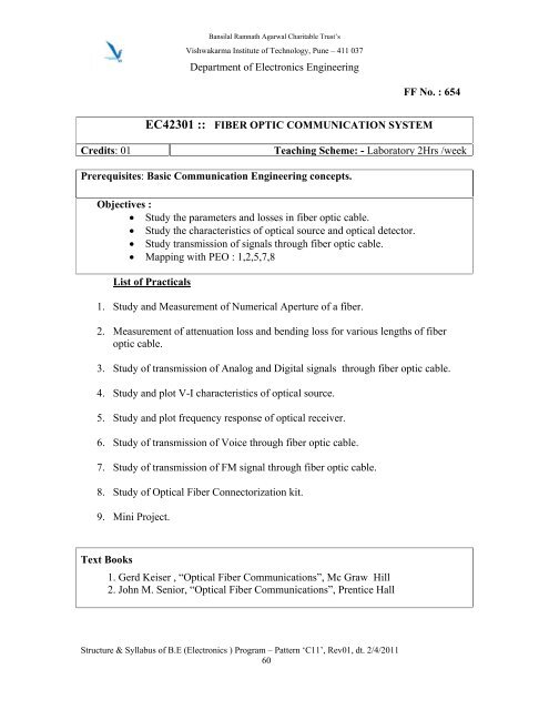
Bansilal Ramnath Agarwal Charitable Trust’s Vishwakarma Institute of Technology, Pune – 411 037 Department of Electronics Engineering FF No. : 654 EC42301 :: FIBER OPTIC COMMUNICATION SYSTEM Credits: 01 Teaching Scheme: - Laboratory 2Hrs /week Prerequisites: Basic Communication Engineering concepts. Objectives : • Study the parameters and losses in fiber optic cable. • Study the characteristics of optical source and optical detector. • Study transmission of signals through fiber optic cable. • Mapping with PEO : 1,2,5,7,8 List of Practicals 1. Study and Measurement of Numerical Aperture of a fiber. 2. Measurement of attenuation loss and bending loss for various lengths of fiber optic cable. 3. Study of transmission of Analog and Digital signals through fiber optic cable. 4. Study and plot V-I characteristics of optical source. 5. Study and plot frequency response of optical receiver. 6. Study of transmission of Voice through fiber optic cable. 7. Study of transmission of FM signal through fiber optic cable. 8. Study of Optical Fiber Connectorization kit. 9. Mini Project. Text Books 1. Gerd Keiser , “Optical Fiber Communications”, Mc Graw Hill 2. John M. Senior, “Optical Fiber Communications”, Prentice Hall Structure & Syllabus of B.E (Electronics ) Program – Pattern ‘C11’, Rev01, dt. 2/4/2011 60
Bansilal Ramnath Agarwal Charitable Trust’s Vishwakarma Institute of Technology, Pune – 411 037 Department of Electronics Engineering FF No. : 654 EC42302:: VLSI DESIGN Credits: 01 Teaching Scheme: - Laboratory 2 Hrs/Week Prerequisites: Nil Objectives: • Design and conduct experiments using SPICE to characterize and optimize digital integrated circuits. • Design, Verify, Analyze and Evaluate the performance (speed, Power, Area, Noise margins of different MOS digital integrated circuits for different design specifications. • Use CAD tool in the design and verification of digital integrated circuits. • Mapping with PEO : 2,3,5,6,7,8,9 List of Practical I-V characteristics of MOS using SPICE To simulate MOS as a switch To simulate Current mirror To simulate Differential Amplifier To simulate Adder. To simulate Latch. To draw the layout of CMOS inverter. To draw the layout of two input logic gate. Course project based on Spice and/or Layout tool Text Books 1. “Digital Integrated Circuits: A Design Perspective”, J. Rabaey, Prentice Hall India. 2. “CMOS analog circuit Design”, P.E. Allen and D.r. Holberg, second Edition, Oxford. 3. “VLSI Technology”, S.M.Sze, , TMH. Reference Books 1. “Principles of CMOS VLSI Design”, N. Weste and K. Eshranghian, Addison Wesley. 2. “CMOS”, RJ Baker, Wiley IEEE Press, 2004. Structure & Syllabus of B.E (Electronics ) Program – Pattern ‘C11’, Rev01, dt. 2/4/2011 61
- Page 9 and 10: Bansilal Ramnath Agarwal Charitable
- Page 11 and 12: Bansilal Ramnath Agarwal Charitable
- Page 13 and 14: Bansilal Ramnath Agarwal Charitable
- Page 15 and 16: Bansilal Ramnath Agarwal Charitable
- Page 17 and 18: Bansilal Ramnath Agarwal Charitable
- Page 19 and 20: Bansilal Ramnath Agarwal Charitable
- Page 21 and 22: Bansilal Ramnath Agarwal Charitable
- Page 23 and 24: Bansilal Ramnath Agarwal Charitable
- Page 25 and 26: Bansilal Ramnath Agarwal Charitable
- Page 27 and 28: Bansilal Ramnath Agarwal Charitable
- Page 29 and 30: Bansilal Ramnath Agarwal Charitable
- Page 31 and 32: Bansilal Ramnath Agarwal Charitable
- Page 33 and 34: Bansilal Ramnath Agarwal Charitable
- Page 35 and 36: Structure, B.E. (Module VII) Subjec
- Page 37 and 38: Bansilal Ramnath Agarwal Charitable
- Page 39 and 40: Bansilal Ramnath Agarwal Charitable
- Page 41 and 42: Bansilal Ramnath Agarwal Charitable
- Page 43 and 44: Unit III Practical Radar considerat
- Page 45 and 46: Bansilal Ramnath Agarwal Charitable
- Page 47 and 48: Bansilal Ramnath Agarwal Charitable
- Page 49 and 50: Bansilal Ramnath Agarwal Charitable
- Page 51 and 52: Bansilal Ramnath Agarwal Charitable
- Page 53 and 54: Bansilal Ramnath Agarwal Charitable
- Page 55 and 56: Bansilal Ramnath Agarwal Charitable
- Page 57 and 58: Bansilal Ramnath Agarwal Charitable
- Page 59: Bansilal Ramnath Agarwal Charitable
- Page 63 and 64: Bansilal Ramnath Agarwal Charitable
- Page 65 and 66: Structure, B.E. (Module VIII) Bansi
- Page 67 and 68: BRACT’S Vishwakarma Institute of
- Page 69 and 70: BRACT’S Vishwakarma Institute of
- Page 71 and 72: BRACT’S Vishwakarma Institute of
- Page 73 and 74: BRACT’S Vishwakarma Institute of
- Page 75 and 76: BRACT’S Vishwakarma Institute of
- Page 77 and 78: BRACT’S Vishwakarma Institute of
- Page 79 and 80: BRACT’S Vishwakarma Institute of
- Page 81 and 82: BRACT’S Vishwakarma Institute of
- Page 83 and 84: BRACT’S Vishwakarma Institute of
- Page 85 and 86: BRACT’S Vishwakarma Institute of
- Page 87 and 88: BRACT’S Vishwakarma Institute of
- Page 89 and 90: BRACT’S Vishwakarma Institute of
- Page 91 and 92: BRACT’S Vishwakarma Institute of
- Page 93 and 94: BRACT’S Vishwakarma Institute of
- Page 95 and 96: BRACT’S Vishwakarma Institute of
- Page 97 and 98: BRACT’S Vishwakarma Institute of
- Page 99 and 100: BRACT’S Vishwakarma Institute of
- Page 101 and 102: BRACT’S Vishwakarma Institute of
- Page 103 and 104: BRACT’S Vishwakarma Institute of
- Page 105 and 106: BRACT’S Vishwakarma Institute of
- Page 107: BRACT’S Vishwakarma Institute of
Bansilal Ramnath Agarwal Charitable Trust’s<br />
<strong>Vishwakarma</strong> <strong>Institute</strong> <strong>of</strong> <strong>Technology</strong>, Pune – 411 037<br />
Department <strong>of</strong> <strong>Electronics</strong> Engineering<br />
FF No. : 654<br />
EC42301 :: FIBER OPTIC COMMUNICATION SYSTEM<br />
Credits: 01<br />
Teaching Scheme: - Laboratory 2Hrs /week<br />
Prerequisites: Basic Communication Engineering concepts.<br />
Objectives :<br />
• Study the parameters and losses in fiber optic cable.<br />
• Study the characteristics <strong>of</strong> optical source and optical detector.<br />
• Study transmission <strong>of</strong> signals through fiber optic cable.<br />
• Mapping with PEO : 1,2,5,7,8<br />
List <strong>of</strong> Practicals<br />
1. Study and Measurement <strong>of</strong> Numerical Aperture <strong>of</strong> a fiber.<br />
2. Measurement <strong>of</strong> attenuation loss and bending loss for various lengths <strong>of</strong> fiber<br />
optic cable.<br />
3. Study <strong>of</strong> transmission <strong>of</strong> Analog and Digital signals through fiber optic cable.<br />
4. Study and plot V-I characteristics <strong>of</strong> optical source.<br />
5. Study and plot frequency response <strong>of</strong> optical receiver.<br />
6. Study <strong>of</strong> transmission <strong>of</strong> Voice through fiber optic cable.<br />
7. Study <strong>of</strong> transmission <strong>of</strong> FM signal through fiber optic cable.<br />
8. Study <strong>of</strong> Optical Fiber Connectorization kit.<br />
9. Mini Project.<br />
Text Books<br />
1. Gerd Keiser , “Optical Fiber Communications”, Mc Graw Hill<br />
2. John M. Senior, “Optical Fiber Communications”, Prentice Hall<br />
Structure & Syllabus <strong>of</strong> B.E (<strong>Electronics</strong> ) Program – Pattern ‘C11’, Rev01, dt. 2/4/2011<br />
60


