Vishwakarma Institute of Technology B.E. (Electronics)
Vishwakarma Institute of Technology B.E. (Electronics) Vishwakarma Institute of Technology B.E. (Electronics)
Bansilal Ramnath Agarwal Charitable Trust’s Vishwakarma Institute of Technology, Pune – 411 037 Department of Electronics Engineering $ Please Refer Academic Information ! Please Refer F.Y. B.Tech. Structure and Syllabi Booklet @ Please Refer GP-PD-OE Structure & Syllabi Booklet Structure & Syllabus of B.E (Electronics ) Program – Pattern ‘C11’, Rev01, dt. 2/4/2011 4
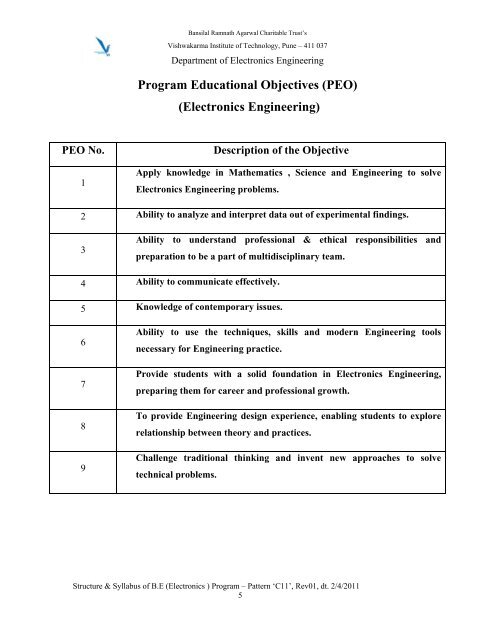
Bansilal Ramnath Agarwal Charitable Trust’s Vishwakarma Institute of Technology, Pune – 411 037 Department of Electronics Engineering Program Educational Objectives (PEO) (Electronics Engineering) PEO No. 1 Description of the Objective Apply knowledge in Mathematics , Science and Engineering to solve Electronics Engineering problems. 2 Ability to analyze and interpret data out of experimental findings. 3 Ability to understand professional & ethical responsibilities and preparation to be a part of multidisciplinary team. 4 Ability to communicate effectively. 5 Knowledge of contemporary issues. 6 7 8 9 Ability to use the techniques, skills and modern Engineering tools necessary for Engineering practice. Provide students with a solid foundation in Electronics Engineering, preparing them for career and professional growth. To provide Engineering design experience, enabling students to explore relationship between theory and practices. Challenge traditional thinking and invent new approaches to solve technical problems. Structure & Syllabus of B.E (Electronics ) Program – Pattern ‘C11’, Rev01, dt. 2/4/2011 5
- Page 1 and 2: Bansilal Ramnath Agarwal Charitable
- Page 3: Bansilal Ramnath Agarwal Charitable
- Page 7 and 8: Structure, T.E. (Module V) Subject
- Page 9 and 10: Bansilal Ramnath Agarwal Charitable
- Page 11 and 12: Bansilal Ramnath Agarwal Charitable
- Page 13 and 14: Bansilal Ramnath Agarwal Charitable
- Page 15 and 16: Bansilal Ramnath Agarwal Charitable
- Page 17 and 18: Bansilal Ramnath Agarwal Charitable
- Page 19 and 20: Bansilal Ramnath Agarwal Charitable
- Page 21 and 22: Bansilal Ramnath Agarwal Charitable
- Page 23 and 24: Bansilal Ramnath Agarwal Charitable
- Page 25 and 26: Bansilal Ramnath Agarwal Charitable
- Page 27 and 28: Bansilal Ramnath Agarwal Charitable
- Page 29 and 30: Bansilal Ramnath Agarwal Charitable
- Page 31 and 32: Bansilal Ramnath Agarwal Charitable
- Page 33 and 34: Bansilal Ramnath Agarwal Charitable
- Page 35 and 36: Structure, B.E. (Module VII) Subjec
- Page 37 and 38: Bansilal Ramnath Agarwal Charitable
- Page 39 and 40: Bansilal Ramnath Agarwal Charitable
- Page 41 and 42: Bansilal Ramnath Agarwal Charitable
- Page 43 and 44: Unit III Practical Radar considerat
- Page 45 and 46: Bansilal Ramnath Agarwal Charitable
- Page 47 and 48: Bansilal Ramnath Agarwal Charitable
- Page 49 and 50: Bansilal Ramnath Agarwal Charitable
- Page 51 and 52: Bansilal Ramnath Agarwal Charitable
- Page 53 and 54: Bansilal Ramnath Agarwal Charitable
Bansilal Ramnath Agarwal Charitable Trust’s<br />
<strong>Vishwakarma</strong> <strong>Institute</strong> <strong>of</strong> <strong>Technology</strong>, Pune – 411 037<br />
Department <strong>of</strong> <strong>Electronics</strong> Engineering<br />
Program Educational Objectives (PEO)<br />
(<strong>Electronics</strong> Engineering)<br />
PEO No.<br />
1<br />
Description <strong>of</strong> the Objective<br />
Apply knowledge in Mathematics , Science and Engineering to solve<br />
<strong>Electronics</strong> Engineering problems.<br />
2 Ability to analyze and interpret data out <strong>of</strong> experimental findings.<br />
3<br />
Ability to understand pr<strong>of</strong>essional & ethical responsibilities and<br />
preparation to be a part <strong>of</strong> multidisciplinary team.<br />
4 Ability to communicate effectively.<br />
5 Knowledge <strong>of</strong> contemporary issues.<br />
6<br />
7<br />
8<br />
9<br />
Ability to use the techniques, skills and modern Engineering tools<br />
necessary for Engineering practice.<br />
Provide students with a solid foundation in <strong>Electronics</strong> Engineering,<br />
preparing them for career and pr<strong>of</strong>essional growth.<br />
To provide Engineering design experience, enabling students to explore<br />
relationship between theory and practices.<br />
Challenge traditional thinking and invent new approaches to solve<br />
technical problems.<br />
Structure & Syllabus <strong>of</strong> B.E (<strong>Electronics</strong> ) Program – Pattern ‘C11’, Rev01, dt. 2/4/2011<br />
5


