Vishwakarma Institute of Technology B.E. (Electronics)
Vishwakarma Institute of Technology B.E. (Electronics)
Vishwakarma Institute of Technology B.E. (Electronics)

Create successful ePaper yourself
Turn your PDF publications into a flip-book with our unique Google optimized e-Paper software.
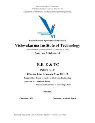
Bansilal Ramnath Agarwal Charitable Trust’s<br />
<strong>Vishwakarma</strong> <strong>Institute</strong> <strong>of</strong> <strong>Technology</strong>, Pune – 411 037<br />
Department <strong>of</strong> <strong>Electronics</strong> Engineering<br />
Bansilal Ramnath Agarwal Charitable Trust’s<br />
<strong>Vishwakarma</strong> <strong>Institute</strong> <strong>of</strong> <strong>Technology</strong><br />
(An Autonomous <strong>Institute</strong> affiliated to University <strong>of</strong> Pune)<br />
Structure & Syllabus <strong>of</strong><br />
B.E. (<strong>Electronics</strong>)<br />
Pattern ‘C11’<br />
Effective from Academic Year 2011-12<br />
Prepared by: - Board <strong>of</strong> Studies in <strong>Electronics</strong> Engineering<br />
Approved by: - Academic Board,<br />
<strong>Vishwakarma</strong> <strong>Institute</strong> <strong>of</strong> <strong>Technology</strong>, Pune<br />
Signed by,<br />
Chairman – BOS<br />
Chairman – Academic Board<br />
Structure & Syllabus <strong>of</strong> B.E (<strong>Electronics</strong> ) Program – Pattern ‘C11’, Rev01, dt. 2/4/2011<br />
1
Bansilal Ramnath Agarwal Charitable Trust’s<br />
<strong>Vishwakarma</strong> <strong>Institute</strong> <strong>of</strong> <strong>Technology</strong>, Pune – 411 037<br />
Department <strong>of</strong> <strong>Electronics</strong> Engineering<br />
Content<br />
Sr. No. Title Page No.<br />
1 Program Educational Objectives 5<br />
2 Module V 6<br />
3 Course Structure 7<br />
4 Course Syllabi For Courses - Module V<br />
Theory Course<br />
4.1 EC30101 Microcontroller & Applications 8<br />
4.2 EC30102 Digital Communication 10<br />
4.3 EC30103 Digital Signal Processing 12<br />
4.4 EC31101 Mechatronics (MD) 14<br />
Tutorial<br />
4.5 EC30201 Digital Communication Microcontroller & 16<br />
4.6 EC30202 Digital Communication 17<br />
Practicals<br />
4.7 EC30301 Microcontroller & Mechatronics Lab 18<br />
4.8 EC30302 Signal Processing And Communication Lab. 19<br />
4.9 EC37401 $ Mini Project<br />
4.10 @ Pr<strong>of</strong>essional Development Course<br />
4.11 EC30401 $ Comprehensive Viva Voce<br />
4.12 EC37301 $ Seminar<br />
Module VI 20<br />
5 Course Structure 21<br />
6 Course Syllabi For Courses – Module VI<br />
Theory Course<br />
6.1 EC30104 Electromagnetic Engineering 22<br />
6.2 EC30108 Linear Integrated circuits & Applications 24<br />
6.3 EC30106 Power <strong>Electronics</strong> 26<br />
6.4 EC30107 Digital Integrated Circuits 28<br />
Tutorial<br />
6.5 EC30203 Electromagnetic Engineering 30<br />
6.6 EC30205 Linear Integrated circuits & Applications 31<br />
Practicals<br />
6.7 EC30305 Linear Integrated circuits & Applications 32<br />
6.8 EC30304 Power & Integrated Circuits Lab 33<br />
6.0 EC37402 $ Mini Project<br />
6.10 @ Pr<strong>of</strong>essional Development Course<br />
6.11 EC30402 $ Comprehensive Viva Voce<br />
6.12 EC37302 $ Project Stage I<br />
Module VII 34<br />
7 Course Structure 35<br />
8 Course Syllabi For Courses - Module VII<br />
Theory Course<br />
8.1 EC40101 Electronic Circuit Design 37<br />
Structure & Syllabus <strong>of</strong> B.E (<strong>Electronics</strong> ) Program – Pattern ‘C11’, Rev01, dt. 2/4/2011<br />
2
Bansilal Ramnath Agarwal Charitable Trust’s<br />
<strong>Vishwakarma</strong> <strong>Institute</strong> <strong>of</strong> <strong>Technology</strong>, Pune – 411 037<br />
Department <strong>of</strong> <strong>Electronics</strong> Engineering<br />
8.2 EC40103 Coding & Data Compression 39<br />
Elective I - Theory Course 41<br />
8.3 EC42101 Remote Sensing 42<br />
8.4 EC42102 Artificial Intelligence 44<br />
8.5 EC42103 Pattern Recognition 46<br />
Elective II - Theory Course 48<br />
8.6 EC42104 Fibre Optic Communication 49<br />
8.7 EC42105 VLSI Design 51<br />
8.9 EC42106 Digital Image Processing 53<br />
Tutorial<br />
8.10 EC40201 Electronic Circuit Design 55<br />
8.11 EC42201 Remote Sensing 56<br />
8.12 EC42202 Artificial Intelligence 57<br />
8.13 EC42203 Pattern Recognition 58<br />
Practicals<br />
8.14 EC40301 Coding & Data Compression 59<br />
Practicals – Elective - II<br />
8.15 EC42301 Fibre Optic Communication 60<br />
8.16 EC42302 VLSI Design 61<br />
8.17 EC42303 Digital Image Processing 62<br />
8.18 EC47301 Project Stage - II 63<br />
Module VIII 64<br />
9 Course Structure 65<br />
10 Course Syllabi For Courses - Module VIII<br />
Theory Course<br />
10.1 EC40104 Computer Networks 66<br />
10.2 EC41101 Embedded Systems (MD) 68<br />
Elective III - Theory 70<br />
10.3 EC42107 Microwave Engineering 71<br />
10.4 EC42109 Electronic Automation 73<br />
10.5 EC42110 Artificial Neural Networks And Fuzzy Logic 75<br />
10.6 EC42111 Wireless Sensor Networks 77<br />
Elective IV - Theory Course 79<br />
10.7 EC42112 Audio Video Engineering 80<br />
10.8 EC42113 Advanced Power <strong>Electronics</strong> 82<br />
10.9 EC42114 Biomedical <strong>Electronics</strong> 84<br />
Tutorial<br />
10.10 EC40203 Computer Networks 86<br />
10.11 EC42204 Microwave Engineering 87<br />
10.12 EC42206 Electronic Automation 88<br />
10.13 EC42207 Artificial Neural Networks And Fuzzy Logic 89<br />
10.14 EC42208 Wireless Sensor Networks 90<br />
Practicals<br />
10.15 EC41301 Embedded Systems 91<br />
Practicals – Elective - IV<br />
10.16 EC42304 Audio Video Engineering 92<br />
10.17 EC42305 Advanced Power <strong>Electronics</strong> 93<br />
10.18 EC42306 Biomedical <strong>Electronics</strong> 94<br />
10.19 EC47302 Project Stage-III 95<br />
11 ACADEMIC INFO<br />
Structure & Syllabus <strong>of</strong> B.E (<strong>Electronics</strong> ) Program – Pattern ‘C11’, Rev01, dt. 2/4/2011<br />
3
Bansilal Ramnath Agarwal Charitable Trust’s<br />
<strong>Vishwakarma</strong> <strong>Institute</strong> <strong>of</strong> <strong>Technology</strong>, Pune – 411 037<br />
Department <strong>of</strong> <strong>Electronics</strong> Engineering<br />
$ Please Refer Academic Information<br />
! Please Refer F.Y. B.Tech. Structure and Syllabi Booklet<br />
@ Please Refer GP-PD-OE Structure & Syllabi Booklet<br />
Structure & Syllabus <strong>of</strong> B.E (<strong>Electronics</strong> ) Program – Pattern ‘C11’, Rev01, dt. 2/4/2011<br />
4
Bansilal Ramnath Agarwal Charitable Trust’s<br />
<strong>Vishwakarma</strong> <strong>Institute</strong> <strong>of</strong> <strong>Technology</strong>, Pune – 411 037<br />
Department <strong>of</strong> <strong>Electronics</strong> Engineering<br />
Program Educational Objectives (PEO)<br />
(<strong>Electronics</strong> Engineering)<br />
PEO No.<br />
1<br />
Description <strong>of</strong> the Objective<br />
Apply knowledge in Mathematics , Science and Engineering to solve<br />
<strong>Electronics</strong> Engineering problems.<br />
2 Ability to analyze and interpret data out <strong>of</strong> experimental findings.<br />
3<br />
Ability to understand pr<strong>of</strong>essional & ethical responsibilities and<br />
preparation to be a part <strong>of</strong> multidisciplinary team.<br />
4 Ability to communicate effectively.<br />
5 Knowledge <strong>of</strong> contemporary issues.<br />
6<br />
7<br />
8<br />
9<br />
Ability to use the techniques, skills and modern Engineering tools<br />
necessary for Engineering practice.<br />
Provide students with a solid foundation in <strong>Electronics</strong> Engineering,<br />
preparing them for career and pr<strong>of</strong>essional growth.<br />
To provide Engineering design experience, enabling students to explore<br />
relationship between theory and practices.<br />
Challenge traditional thinking and invent new approaches to solve<br />
technical problems.<br />
Structure & Syllabus <strong>of</strong> B.E (<strong>Electronics</strong> ) Program – Pattern ‘C11’, Rev01, dt. 2/4/2011<br />
5
Bansilal Ramnath Agarwal Charitable Trust’s<br />
<strong>Vishwakarma</strong> <strong>Institute</strong> <strong>of</strong> <strong>Technology</strong>, Pune – 411 037<br />
Department <strong>of</strong> <strong>Electronics</strong> Engineering<br />
- V<br />
Structure & Syllabus <strong>of</strong> B.E (<strong>Electronics</strong> ) Program – Pattern ‘C11’, Rev01, dt. 2/4/2011<br />
6<br />
MODULE
Structure, T.E. (Module V)<br />
Subject<br />
No.<br />
Subject<br />
Code<br />
Bansilal Ramnath Agarwal Charitable Trust’s<br />
<strong>Vishwakarma</strong> <strong>Institute</strong> <strong>of</strong> <strong>Technology</strong>, Pune – 411 037<br />
Department <strong>of</strong> <strong>Electronics</strong> Engineering<br />
FF653, Issue No. 3, Rev 1, dt 02/04/2011<br />
Subject Name Teaching Scheme (Hrs/week) Credits<br />
Lect. Tutorial Practical<br />
S 1 EC30101 Microcontroller & Applications 3 0 0 3<br />
S 2 EC30102 Digital Communication 3 0 0 3<br />
S 3 EC30103 Digital Signal Processing 3 0 0 3<br />
S 4 EC31101 Mechatronics (MD) 3 0 0 3<br />
T 1 EC30201 Microcontroller & Applications 0 1 0 1<br />
T 2 EC30202 Digital Communication 0 1 0 1<br />
P 1 EC30301 Microcontroller & Mechatronics Lab. 0 0 2 1<br />
P 2 EC30302 Signal Processing and Communication Lab. 0 0 2 1<br />
MP 5 EC37401 Mini Project 0 0 2 1<br />
* PD 1 EC333XX <strong>Institute</strong> Level Elective 0 0 2 1<br />
CVV 3 EC30401 Comprehensive Viva Voce Based on Courses S1 & S3 1<br />
SM 1 EC37301 Seminar 0 0 2 2<br />
Total 12 2 10 21<br />
Structure & Syllabus <strong>of</strong> B.E (<strong>Electronics</strong> ) Program – Pattern ‘C11’, Rev01, dt. 2/4/2011<br />
7
Bansilal Ramnath Agarwal Charitable Trust’s<br />
<strong>Vishwakarma</strong> <strong>Institute</strong> <strong>of</strong> <strong>Technology</strong>, Pune – 411 037<br />
Department <strong>of</strong> <strong>Electronics</strong> Engineering<br />
FF No. : 654<br />
EC30101:: MICROCONTROLLER AND APPLICATIONS<br />
Credits: 03<br />
Teaching Scheme: - Theory 3 Hrs/Week<br />
Prerequisites: Concepts <strong>of</strong> digital electronics, C language programming<br />
Objectives:<br />
To study<br />
• Architecture <strong>of</strong> 80C51microcontroller<br />
• Interfacing <strong>of</strong> peripherals to microcontroller<br />
• Assembly language and embedded C language programming.<br />
• Serial communication protocols.<br />
• RISC microcontrollers.<br />
• Mapping with PEO : 3,6,7,8,9<br />
Unit I<br />
(8 Hrs)<br />
INTRODUCTION TO MICROCONTROLLER<br />
A. Microprocessor and microcontroller, Features and architecture <strong>of</strong> 80C51<br />
microcontroller, Addressing modes , Instruction set<br />
B. Features and architecture <strong>of</strong> 89V51RD2 microcontroller<br />
Unit II<br />
ONCHIP PERIPHERALS OF 80C51<br />
(8 Hrs)<br />
A. Port structure, Timers and counters, Serial port, Interrupt structure and simple<br />
assembly language program<br />
B. On chip peripherals <strong>of</strong> 89V51RD2( PCA with PWM, Timers and counters, Interrupts<br />
etc)<br />
Unit III<br />
SERIAL AND PARALLEL PORT INTERFACING<br />
(9 Hrs)<br />
A. Interfacing <strong>of</strong> display devices like LED, Seven segment, 2 x 16 character LCD (8bit<br />
mode),serial communication protocols-RS232, RS485, Buses-I2C and its implementation<br />
, SPI<br />
B. Interfacing <strong>of</strong> 2 x 16 character LCD (4bit mode)<br />
Structure & Syllabus <strong>of</strong> B.E (<strong>Electronics</strong> ) Program – Pattern ‘C11’, Rev01, dt. 2/4/2011<br />
8
Bansilal Ramnath Agarwal Charitable Trust’s<br />
<strong>Vishwakarma</strong> <strong>Institute</strong> <strong>of</strong> <strong>Technology</strong>, Pune – 411 037<br />
Department <strong>of</strong> <strong>Electronics</strong> Engineering<br />
Unit IV<br />
INTERFACING AND PROGRAMMING USING EMBEDDED C<br />
(8 Hrs)<br />
A. 4 X 4 matrix keypad, DAC( Binary weighted and R2R ladder), ADC(Dual slope and<br />
Successive approximation type), Stepper motor( Unipolar, permanent magnet)<br />
B. Interfacing <strong>of</strong> relay and DC motor<br />
Unit V<br />
RISC MICROCONTROLLERS<br />
(7 Hrs)<br />
A. Memory interfacing, Features and Architecture <strong>of</strong> PIC 16F877A and AVR Atmega32,<br />
Theoretical minimum system design.<br />
B.Instruction set <strong>of</strong> PIC 16F877A<br />
Outcomes<br />
After studying the syllabus, students will be able to<br />
1) Write Assembly and C language Program for 8051<br />
2) Interface various peripheral devices to 8051<br />
Text Books<br />
1. ‘8051 and Embedded C programming’- Mazidi and Mazidi, Second edition, Pearson<br />
education<br />
2. ‘8051 microcontroller Architecture, programming and Applications- Kenath Ayala,<br />
third edition, Peneram publication<br />
References<br />
1. Datasheets <strong>of</strong> 89C51RD2, ADC 0809,DAC 0808, PIC 16F877A, AVR Atmega32,<br />
PCF 8591<br />
2. ‘Serial port complete’- Jan Axelson, Peneram publication<br />
Structure & Syllabus <strong>of</strong> B.E (<strong>Electronics</strong> ) Program – Pattern ‘C11’, Rev01, dt. 2/4/2011<br />
9
Bansilal Ramnath Agarwal Charitable Trust’s<br />
<strong>Vishwakarma</strong> <strong>Institute</strong> <strong>of</strong> <strong>Technology</strong>, Pune – 411 037<br />
Department <strong>of</strong> <strong>Electronics</strong> Engineering<br />
FF No. : 654<br />
EC30102 :: DIGITAL COMMUNICATION<br />
Credits: 03<br />
Teaching Scheme: - Theory 3 Hrs/Week<br />
Prerequisites: Fourier series, Fourier transform, probability theory, Analog<br />
communication<br />
Objectives:<br />
To study-<br />
• The basics <strong>of</strong> Sampling Theorem & Aliasing Effect<br />
• Digital Communication Techniques<br />
• Spread Spectrum Techniques<br />
• Mapping with PEO : 1,2,3,6,7,8,9<br />
Unit I<br />
Sampling & Waveform Coding<br />
(8 Hrs)<br />
A Introduction to digital communication, Sampling, reconstruction, ideal sampling, Flat<br />
top & Natural Sampling Aliasing, Aperture effect. Pulse code modulation &<br />
reconstruction, Quantization noise, Companded PCM, Delta modulation, Adaptive delta<br />
modulation, Differential PCM, ISI and eye diagram.<br />
B. LPC and Line Coding, equalizers.<br />
Unit II<br />
Digital modulation techniques<br />
(8 Hrs)<br />
A. Digital modulation techniques such as Binary Phase Shift Keying, Quadrature Phase<br />
Shift Keying, M-Ary PSK , Quadrature Amplitude Shift Keying, Binary Frequency Shift<br />
Keying, M-Ary Frequency Shift Keying, Minimum Shift Keying<br />
B. Differential Phase Shift Keying, Differentially encoded PSK , Gaussian Minimum<br />
Shift Keying.<br />
Unit III<br />
(8 Hrs)<br />
Detection & Performance Analysis Of Digital Signal<br />
A.Base Band signal receiver ,Derivation for Error prob <strong>of</strong> int. & dump Filter, Optimum<br />
Filter, white noise matched filter, probability error <strong>of</strong> match filter, correlation, FSK, PSK,<br />
non- coherent detection <strong>of</strong> FSK, DPSK, QPSK, Calculation <strong>of</strong> error probability for BPSK<br />
& BFSK , Signal Space to calculate Probability <strong>of</strong> error.<br />
B Correlator receiver.<br />
Structure & Syllabus <strong>of</strong> B.E (<strong>Electronics</strong> ) Program – Pattern ‘C11’, Rev01, dt. 2/4/2011<br />
10
Bansilal Ramnath Agarwal Charitable Trust’s<br />
<strong>Vishwakarma</strong> <strong>Institute</strong> <strong>of</strong> <strong>Technology</strong>, Pune – 411 037<br />
Department <strong>of</strong> <strong>Electronics</strong> Engineering<br />
Unit IV<br />
(8 Hrs)<br />
Spread Spectrum<br />
A. Pusedo-random Sequence, Direct Sequence Spread Spectrum Phase Shift Keying<br />
block details & mathematical treatment , Power Spectrum Density curves, Jamming<br />
margin and processing gain, Probability <strong>of</strong> error, Frequency Hop Spread Spectrum.<br />
B. applications <strong>of</strong> DSSSPSK and FHSS<br />
Unit V<br />
Introduction to Link Design and Link Budget Analysis<br />
(8 Hrs)<br />
A. CDMA,TDMA,FDMA, Kepler’s Laws, Satellite orbits, Satellite system link models,<br />
Satellite system parameters and link budget.<br />
B. Geostationary satellites<br />
Text Books<br />
1. Taub Schilling, ‘Principles <strong>of</strong> communication system’, Tata McGraw Hill, 2 nd<br />
Edition<br />
2 . B.Sklar , ‘Digital Communication’, Pearson, 2 nd edition …..<br />
Reference Books<br />
1. Simon Haykin , ‘Digital Communications’, Wiley Publications, 4 th edition<br />
2. Carlson , ‘Communication System’, McGrawHill, 4 th edition<br />
Structure & Syllabus <strong>of</strong> B.E (<strong>Electronics</strong> ) Program – Pattern ‘C11’, Rev01, dt. 2/4/2011<br />
11
Bansilal Ramnath Agarwal Charitable Trust’s<br />
<strong>Vishwakarma</strong> <strong>Institute</strong> <strong>of</strong> <strong>Technology</strong>, Pune – 411 037<br />
Department <strong>of</strong> <strong>Electronics</strong> Engineering<br />
FF No. : 654<br />
EC 30103 :: DIGITAL SIGNAL PROCESSING<br />
Credits: 03<br />
Teaching Scheme: - Theory 3 Hrs/Week<br />
Prerequisites: Knowledge <strong>of</strong> signals and systems, Fourier Theory<br />
Objectives:<br />
• To learn properties <strong>of</strong> discrete time signals and systems<br />
• To learn processing <strong>of</strong> signals in frequency domain using mathematical<br />
transforms<br />
• To learn filter design based on approximations<br />
• To learn filter design based on truncation <strong>of</strong> impulse response<br />
• Mapping with PEO : 1,2, 6,7,8,9<br />
Unit I : Z Transform<br />
(10 Hrs.)<br />
A. Discrete time signals & Systems, Z- transform and its properties, Inverse Z-transform,<br />
analysis <strong>of</strong> LTI systems in Z domain, Unilateral Z-transform.<br />
B. Sampling process, Convolution and Correlation<br />
Unit II : Discrete Fourier Transform<br />
(12+ 1Hrs.)<br />
A. Discrete time Fourier transform(DTFT), Discrete Fourier transform(DFT), Relation <strong>of</strong><br />
DFT to other transforms, Properties <strong>of</strong> DFT, Overlap_add and overlap_save methods,<br />
FFT algorithms- Decimation in Time and Decimation in frequency<br />
B. Goertzel algorithm, applications <strong>of</strong> DFT and FFT<br />
Unit III : FIR Filters<br />
(6 Hrs.)<br />
A. FIR filter structures - Direct form structure, cascade form structure, Design <strong>of</strong> linear<br />
phase FIR filters using windows , Design <strong>of</strong> linear phase FIR filters using frequency<br />
sampling method.<br />
B. Lattice Structure, Design <strong>of</strong> FIR filters using Fourier series method, applications <strong>of</strong><br />
FIR filters<br />
Structure & Syllabus <strong>of</strong> B.E (<strong>Electronics</strong> ) Program – Pattern ‘C11’, Rev01, dt. 2/4/2011<br />
12
Bansilal Ramnath Agarwal Charitable Trust’s<br />
<strong>Vishwakarma</strong> <strong>Institute</strong> <strong>of</strong> <strong>Technology</strong>, Pune – 411 037<br />
Department <strong>of</strong> <strong>Electronics</strong> Engineering<br />
Unit IV : IIR Filters<br />
A. IIR filter structures - Direct form, Parallel form, cascade structure.<br />
IIR Filter design methods - Bilinear transformation, Impulse invariance<br />
B. IIR Filter design by Approximation <strong>of</strong> Derivatives.<br />
(6 Hrs.)<br />
Unit V : Finite Word Length Effects<br />
(6 Hrs.)<br />
A. Rounding and Truncation errors, Coefficient Quantization effects in FIR and IIR<br />
filters,Limit Cycle Oscillations, Product Quantization<br />
B. Quantization Errors in DFT Computaions and FFT algorithms.<br />
Text Books<br />
1. Sanjit Mitra, ‘Digital Signal Processing’, TMH, 3 rd edition<br />
2. John Proakis, Dimitri Manolakis, ‘Digital Signal Processing – Principles,<br />
Algorithms & Applications’, PHI<br />
Reference Books<br />
1. Ramesh Babu, ‘Digital Signal Processing’ , Scitech publications, 2001<br />
2. Shalivahanan, Vallavraj, Gnanapriya C., ‘Digital Signal Processing’, TMH, 2001<br />
Structure & Syllabus <strong>of</strong> B.E (<strong>Electronics</strong> ) Program – Pattern ‘C11’, Rev01, dt. 2/4/2011<br />
13
Bansilal Ramnath Agarwal Charitable Trust’s<br />
<strong>Vishwakarma</strong> <strong>Institute</strong> <strong>of</strong> <strong>Technology</strong>, Pune – 411 037<br />
Department <strong>of</strong> <strong>Electronics</strong> Engineering<br />
FF No. : 654<br />
Credits: 03<br />
EC31101:: MECHATRONICS<br />
Teaching Scheme: - Theory 3 Hrs/Week<br />
Prerequisites: Basics <strong>of</strong> Op-Amp, Network theory, Control system<br />
Objectives:<br />
• Understand the synergistic integration <strong>of</strong> multidisciplinary engineering.<br />
• Understand the key elements <strong>of</strong> measurement system.<br />
• Be able to design mechatronics system.<br />
• Mapping with PEO : 1,3,5,6,7,8,9<br />
Unit I<br />
(8 Hrs)<br />
Unit Name: Introduction to Mechatronics<br />
A. Scope & importance <strong>of</strong> Mechatronics with respect to interdisciplinary approach Roll<br />
<strong>of</strong> <strong>Electronics</strong> in Mechatronics, Mathematical Modeling <strong>of</strong> Physical Systems: -<br />
Mechanical, Electrical, Thermal, and Fluid.<br />
B. Study <strong>of</strong> automated systems- Industrial robots, Automatic weighing machine.<br />
Unit II<br />
Unit Name: Sensors and Transducers<br />
(8 Hrs)<br />
A. Static & dynamic Characteristics <strong>of</strong> Sensors and Systems, Performance Terminology<br />
<strong>of</strong> sensors (Selection criteria <strong>of</strong> sensors), Study <strong>of</strong> Temperature, pressure and force,<br />
motion, proximity, displacement, flow sensors.<br />
B. Vibration, Range Sensors<br />
Unit III<br />
Unit Name: Signal Conditioning<br />
Structure & Syllabus <strong>of</strong> B.E (<strong>Electronics</strong> ) Program – Pattern ‘C11’, Rev01, dt. 2/4/2011<br />
14<br />
(8 Hrs)<br />
A. Importance <strong>of</strong> signal conditioning, Use <strong>of</strong> AC and DC bridges, filters, Operational<br />
Amplifier circuits, Overview <strong>of</strong> ADC and DAC, and its selection criteria.<br />
B. Types <strong>of</strong> ADC & DAC<br />
Unit IV<br />
Unit Name: Actuators<br />
(8 Hrs)<br />
A. Introduction to Pneumatic and Hydraulic systems, Linear and Rotary actuators,<br />
Control valves, Electrical actuators – relay, solenoid, and stepper motor, servomotor.
Bansilal Ramnath Agarwal Charitable Trust’s<br />
<strong>Vishwakarma</strong> <strong>Institute</strong> <strong>of</strong> <strong>Technology</strong>, Pune – 411 037<br />
Department <strong>of</strong> <strong>Electronics</strong> Engineering<br />
B. Mechanical Actuating Systems<br />
Unit V<br />
Unit Name: Data Acquisition and PLC<br />
(8 Hrs)<br />
A. Elements <strong>of</strong> Data Acquisition, Types and selection criteria <strong>of</strong> key components in DAS.<br />
Introduction to PLC-Basic Architecture, I/O Processing, Ladder Programming,<br />
Interfacing <strong>of</strong> sensors and actuators to PLC.<br />
B. Specification and selection <strong>of</strong> PLC, Microcontroller Interfacing, Development Tools.<br />
Outcomes:<br />
Upon completion <strong>of</strong> this course, students will be able to:<br />
• Design signal conditioning circuit.<br />
• Design Data Acquisition System.<br />
• Design Mechatronics system.<br />
Text Books<br />
1. W. Boltan, ‘Mechatronics’. Pearson education, 3 rd edition.<br />
2. Devdas Shetty, ‘Mechatronics Systems Design’ Thomson publication.<br />
Reference Books<br />
1. Rangan,Mani,Sarma, ‘Instrumentation Devices & Systems’, Tata Mcgraw Hill,<br />
2 nd edition.<br />
2. A.K Sawhney, ‘Electrical and Electronic Measurement and Instrumentation’,<br />
Dhanapat Rai and Co., 7 th edition.<br />
3. K.P.Ramchandran, ‘Mechatronics- Integrated Mechanical Electronic Systems’,<br />
Wiley India.<br />
4. N.P. Mahalik, ‘Mechatronics Principles, Concepts & Applications’, Tata Mcgraw<br />
Hill, 2 nd Edition<br />
Structure & Syllabus <strong>of</strong> B.E (<strong>Electronics</strong> ) Program – Pattern ‘C11’, Rev01, dt. 2/4/2011<br />
15
Bansilal Ramnath Agarwal Charitable Trust’s<br />
<strong>Vishwakarma</strong> <strong>Institute</strong> <strong>of</strong> <strong>Technology</strong>, Pune – 411 037<br />
Department <strong>of</strong> <strong>Electronics</strong> Engineering<br />
FF No. : 654<br />
EC 30201: MICROCONTROLLER AND APPLICATIONS<br />
Credits: 1<br />
Tutorials - 1 Hr/Week<br />
Mapping with PEO : 3,6,7,8,9<br />
List <strong>of</strong> Tutorials<br />
1. Assembly language program for unsigned arithmetic operations.<br />
2. Assembly language program for multibyte addition.<br />
3. Assembly language program for block transfer.<br />
4. Assembly language program to find Largest/smallest number from a given array<br />
5. Implementation <strong>of</strong> Boolean expression<br />
6. Interfacing switches and LEDs and its Assembly language program<br />
7. PWM generation<br />
8. Assembly language program using interrupts<br />
9. Seven segment display interfacing and its programming in assembly language<br />
10. 4 X 4 matrix keypad interfacing and its programming in embedded C language<br />
11. Implementation <strong>of</strong> I2C protocol.<br />
12. Stepper motor interfacing and its program in embedded C language<br />
Text Books<br />
3. ‘8051 and Embedded C programming’- Mazidi and Mazidi, Second edition, Pearson<br />
education<br />
4. ‘8051 microcontroller Architecture, programming and Applications- Kenath Ayala,<br />
third edition, Peneram publication<br />
References<br />
3. Datasheets <strong>of</strong> 89C51RD2, ADC 0809,DAC 0808, PIC 16F877A, AVR Atmega32,<br />
PCF 8591<br />
4. ‘Serial port complete’- Jan Axelson, Peneram publication<br />
Structure & Syllabus <strong>of</strong> B.E (<strong>Electronics</strong> ) Program – Pattern ‘C11’, Rev01, dt. 2/4/2011<br />
16
Bansilal Ramnath Agarwal Charitable Trust’s<br />
<strong>Vishwakarma</strong> <strong>Institute</strong> <strong>of</strong> <strong>Technology</strong>, Pune – 411 037<br />
Department <strong>of</strong> <strong>Electronics</strong> Engineering<br />
FF No. : 654<br />
EC30202 :: DIGITAL COMMUNICATION<br />
Credits: 01<br />
Tutorials - 1 Hr/Week<br />
Prerequisites: Fourier series, Fourier transform, probability theory, Analog<br />
communication<br />
Objectives:<br />
To study<br />
• The basics <strong>of</strong> Sampling Theorem & Aliasing Effect<br />
• Digital Communication Techniques<br />
• Spread Spectrum Techniques<br />
• Mapping with PEO : 1,2,3,6,7,8,9<br />
List <strong>of</strong> Tutorials<br />
1. PAM- TDM<br />
2. Code Modulation.<br />
3. Pulse Code Modulation Companding.<br />
4. Differential PCM<br />
5. Adaptive Delta Modulation<br />
6. Study <strong>of</strong> data formats.<br />
7. To Study BPSK<br />
8. To Study QAM.<br />
9. PN Sequence Generator<br />
10. Study <strong>of</strong> FHSS<br />
11. Study <strong>of</strong> Satellite Receiver.<br />
12. GMSK<br />
Text Books<br />
1. Taub Schilling, ‘Principles <strong>of</strong> communication system’, Tata McGraw Hill, 2 nd<br />
Edition<br />
2 . B.Sklar , ‘Digital Communication’, Pearson, 2 nd edition …..<br />
Reference Books<br />
3. Simon Haykin , ‘Digital Communications’, Wiley Publications, 4 th edition<br />
4. Carlson , ‘Communication System’, McGrawHill, 4 th edition<br />
Structure & Syllabus <strong>of</strong> B.E (<strong>Electronics</strong> ) Program – Pattern ‘C11’, Rev01, dt. 2/4/2011<br />
17
Bansilal Ramnath Agarwal Charitable Trust’s<br />
<strong>Vishwakarma</strong> <strong>Institute</strong> <strong>of</strong> <strong>Technology</strong>, Pune – 411 037<br />
Department <strong>of</strong> <strong>Electronics</strong> Engineering<br />
FF No. : 654<br />
EC 30301: MICROCONTROLLER & MECHATRONICS LAB<br />
Credits: 1<br />
Teaching Scheme: - Laboratory 2 Hrs/Week<br />
Part A :: MICROCONTROLLER AND APPLICATIONS<br />
Objectives:<br />
• To interface various peripherals and develop its assembly language and embedded<br />
language program.<br />
• To implement serial communication protocol<br />
• To study sensors and its characteristics.<br />
• To design signal conditioning circuits for sensors.<br />
• To study PLC and its applications.<br />
Mapping with PEO :2,3,6,8,9<br />
List <strong>of</strong> practicals:<br />
1. Arithmetic operations on signed numbers<br />
2. 2 X 16 character LCD interfacing<br />
3. Serial communication interfacing<br />
4. DAC/ADC interfacing<br />
5. Study <strong>of</strong> sensors – Temperature, LVDT, Encoder<br />
6. Study pneumatic actuators.<br />
7. Study <strong>of</strong> PLC – implementation <strong>of</strong> Ladder programming.<br />
8. Study <strong>of</strong> Applications <strong>of</strong> PLC. / Simulation <strong>of</strong> Physical Systems.<br />
9. Mini Project: - Signal conditioning <strong>of</strong> Sensors, Interfacing <strong>of</strong> Pneumatic<br />
Components to PLC/ other semester – Sensor and Actuators interfacing to 8051<br />
Microcontroller.<br />
Text Books<br />
1. ‘8051 and Embedded C programming’- Mazidi and Mazidi, Second<br />
edition, Pearson education<br />
2. ‘8051 microcontroller Architecture, programming and Applications-<br />
Kenath Ayala, third edition, Peneram publication<br />
3. W. Boltan, ‘Mechatronics’. Pearson education, 3 rd edition.<br />
4. Devdas Shetty, ‘Mechatronics Systems Design’ Thomson publication.<br />
Structure & Syllabus <strong>of</strong> B.E (<strong>Electronics</strong> ) Program – Pattern ‘C11’, Rev01, dt. 2/4/2011<br />
18
Bansilal Ramnath Agarwal Charitable Trust’s<br />
<strong>Vishwakarma</strong> <strong>Institute</strong> <strong>of</strong> <strong>Technology</strong>, Pune – 411 037<br />
Department <strong>of</strong> <strong>Electronics</strong> Engineering<br />
FF No. : 654<br />
EC 30302 :: SIGNAL PROCESSING AND COMMUNICATION LAB<br />
Credits: 01<br />
Teaching Scheme: - Practical 2 Hrs/Week<br />
Prerequisites: Knowledge <strong>of</strong> programming language such as MATLAB, Fourier series,<br />
Fourier transform, probability theory, Analog communication<br />
Objectives:<br />
• Implementation <strong>of</strong> Decimation in Time/ Decimation in frequency FFT<br />
• To design FIR and IIR filters<br />
• Real time application on DSP Processor<br />
• Mapping with PEO : 1,2, 6,7,8,9<br />
List <strong>of</strong> Practicals<br />
1. Magnitude and phase spectrum plot.<br />
2. Decimation in Time/ Decimation in frequency FFT.<br />
3. FIR/IIR Filter Design<br />
4. Study <strong>of</strong> finite word length effects in FIR, IIR digital filters.<br />
5. Verification <strong>of</strong> Sampling Theorem (PAM)<br />
6. To Study PCM (Tr & Rx )<br />
7. To Study DM (Tr & Rx )<br />
8. To Study QPSK<br />
9. To Study BFSK<br />
10. To Study DS-SS PSK<br />
11. Mini Project<br />
Text Books<br />
1. Sanjit Mitra, ‘Digital Signal Processing’, TMH, 3 rd edition<br />
2. John Proakis, Dimitri Manolakis, ‘Digital Signal Processing – Principles,<br />
Algorithms & Applications’, PHI<br />
3. Taub Schilling, ‘Principles <strong>of</strong> communication system’, Tata McGraw Hill<br />
4. B.Sklar , ‘Digital Communication’, Pearson, 2 nd edition …..<br />
Structure & Syllabus <strong>of</strong> B.E (<strong>Electronics</strong> ) Program – Pattern ‘C11’, Rev01, dt. 2/4/2011<br />
19
Bansilal Ramnath Agarwal Charitable Trust’s<br />
<strong>Vishwakarma</strong> <strong>Institute</strong> <strong>of</strong> <strong>Technology</strong>, Pune – 411 037<br />
Department <strong>of</strong> <strong>Electronics</strong> Engineering<br />
MODULE - VI<br />
Structure & Syllabus <strong>of</strong> B.E (<strong>Electronics</strong> ) Program – Pattern ‘C11’, Rev01, dt. 2/4/2011<br />
20
Bansilal Ramnath Agarwal Charitable Trust’s<br />
<strong>Vishwakarma</strong> <strong>Institute</strong> <strong>of</strong> <strong>Technology</strong>, Pune – 411 037<br />
Department <strong>of</strong> <strong>Electronics</strong> Engineering<br />
Structure, T.E. (Module VI)<br />
Subject<br />
No.<br />
Subject<br />
Code<br />
FF653, Issue No. 3, Rev 1, dt 02/04/2011<br />
Subject Name Teaching Scheme (Hrs/week) Credits<br />
Lect. Tutorial Practical<br />
S 5 EC30104 Electromagnetic Engineering 3 0 0 3<br />
S 6 EC30108 Linear Integrated Circuits & Applications 3 0 0 3<br />
S 7 EC30106 Power <strong>Electronics</strong> 3 0 0 3<br />
S 8 EC30107 Digital Integrated Circuits 3 0 0 3<br />
T 3 EC30203 Electromagnetic Engineering 0 1 0 1<br />
T 4 EC30205 Linear Integrated Circuits & Applications 0 1 0 1<br />
P 3 EC30305 Linear Integrated Circuits & Applications 0 0 2 1<br />
P 4 EC30304 Power & Integrated Circuits Lab 0 0 2 1<br />
MP 6 EC37402 Mini Project 0 0 2 1<br />
* PD 2 <strong>Institute</strong> Level Elective 0 0 2 1<br />
CVV 4 EC30402 Comprehensive Viva Voce Based on Courses S7 & S8 1<br />
PS 1 EC37302 Project stage - I 0 0 4 2<br />
Total 12 2 12 21<br />
Structure & Syllabus <strong>of</strong> B.E (<strong>Electronics</strong> ) Program – Pattern ‘C11’, Rev01, dt. 2/4/2011<br />
21
Bansilal Ramnath Agarwal Charitable Trust’s<br />
<strong>Vishwakarma</strong> <strong>Institute</strong> <strong>of</strong> <strong>Technology</strong>, Pune – 411 037<br />
Department <strong>of</strong> <strong>Electronics</strong> Engineering<br />
FF No. : 654<br />
EC30104:: ELECTROMAGNETIC ENGINEERING<br />
Credits: 03<br />
Teaching Scheme: - Theory 3 Hrs/Week<br />
Prerequisites: Basics <strong>of</strong> ‘ C’ Programming Language<br />
Objectives:<br />
• To study force experienced by a charge(s) in electrostatic, magnetostatic and<br />
electromagnetic fields<br />
• To study power transmitted by electromagnetic waves in different media<br />
• Mapping with PEO : 1,2, 6,7,8<br />
Unit I<br />
Vectors and Coordinate Systems<br />
(4 Hrs)<br />
A. Addition, subtraction, dot product and vector product <strong>of</strong> vectors, unit vectors,<br />
position and displacement vectors, Cartesian, cylindrical and spherical coordinate<br />
systems<br />
Unit II<br />
Electrostatics<br />
(12 Hrs)<br />
A. Coulomb’s Law, Concept <strong>of</strong> Electric Field intensity, Electric Field Intensity due<br />
to various charge distributions, Gauss’s law and its applications, Divergence<br />
theorem, Work, Energy, Potential, Gradient, Electric Fields in conductors and<br />
dielectrics, Continuity Equation, Boundary Conditions<br />
B. Laplace, Poisson’s equations<br />
Unit III<br />
Applications <strong>of</strong> Linear Data Structures<br />
(10 Hrs)<br />
Structure & Syllabus <strong>of</strong> B.E (<strong>Electronics</strong> ) Program – Pattern ‘C11’, Rev01, dt. 2/4/2011<br />
22
Bansilal Ramnath Agarwal Charitable Trust’s<br />
<strong>Vishwakarma</strong> <strong>Institute</strong> <strong>of</strong> <strong>Technology</strong>, Pune – 411 037<br />
Department <strong>of</strong> <strong>Electronics</strong> Engineering<br />
A. Biot Savart law, Magnetic Field Intensity due to various current distributions,<br />
Ampere’s circuital law and its applications, Curl, Stokes’ theorem, Magnetic Flux<br />
and magnetic flux density, Scalar and vector magnetic potentials, Forces due to<br />
magnetic fields, Magnetization and Permeability, Boundary conditions, Magnetic<br />
Energy<br />
B. Magnetic circuits, Inductance and Mutual Inductance.<br />
Unit IV<br />
Maxwell’s Equations & Time Varying Fields<br />
(8 Hrs)<br />
A. Faraday’s law, Displacement current, Maxwell’s equations, Time varying fields, Time<br />
harmonic fields, Energy stored in electric and magnetic time varying field<br />
B. Retarded potentials<br />
Unit V<br />
Uniform Plane Wave And Propagation<br />
(8 Hrs)<br />
A. Wave equation, Wave propagation in free space, dielectrics and conductors, Skin<br />
Effect, Polarization, Reflection <strong>of</strong> uniform plane waves at normal and oblique<br />
incidence, Standing wave ratio, Wave reflection from multiple interfaces<br />
B. Wave propagation in dispersive media<br />
Text Books<br />
1. Sadiku Matthew N O, ‘Elements <strong>of</strong> Electromagnetics’, Oxford University Press,<br />
3 rd edition, 2002/2003.<br />
2. Hayt W H, ‘Engineering Electromagnetics’, Mc_graw Hill Book Co., 7 th edition,<br />
1981<br />
Reference Books<br />
1. Kruse R L, Leung B P & Tondo C L: Data Structure And Programming Design In<br />
C. Prentice Hall Of<br />
India Pvt.ltd.<br />
2. Kakde O G & Deshpande ,” Data Structures And Algorithms”. Indian Society For<br />
Technical E<br />
3. Sahni S: Data Structures, Algorithms,& Applications In C++. Mcgraw Hill<br />
Boston.<br />
Structure & Syllabus <strong>of</strong> B.E (<strong>Electronics</strong> ) Program – Pattern ‘C11’, Rev01, dt. 2/4/2011<br />
23
Bansilal Ramnath Agarwal Charitable Trust’s<br />
<strong>Vishwakarma</strong> <strong>Institute</strong> <strong>of</strong> <strong>Technology</strong>, Pune – 411 037<br />
Department <strong>of</strong> <strong>Electronics</strong> Engineering<br />
FF No. : 654<br />
EC30108 :: LINEAR INTEGRATED CIRCUITS AND<br />
APPLICATIONS<br />
Credits: 03<br />
Teaching Scheme: - Theory 3 Hrs/Week<br />
Prerequisites:<br />
• Solid State Devices<br />
• <strong>Electronics</strong> Circuits and Applications<br />
Objectives:<br />
• Fundamentals <strong>of</strong> Op-Amp<br />
• Design aspects <strong>of</strong> Op-Amp circuits<br />
• Linear and non-linear applications <strong>of</strong> Op-Amp<br />
• Fundamentals <strong>of</strong> Phase Locked Loop and its Applications<br />
• Mapping with PEO : 1,2,5,6,7,8,9<br />
Unit I: OP-AMP Fundamentals (6+1<br />
Hrs)<br />
A. Basic building blocks <strong>of</strong> operational amplifier, Current sources like Widlar, Active<br />
level shifters, Output Stage, Single supply operation and biasing, open loop and closed<br />
loop operation, Inverting and non-inverting configurations <strong>of</strong> op-amp, Concept <strong>of</strong> virtual<br />
short and virtual ground.<br />
B. Wilson and MOSFET sources<br />
Unit II: OP-AMP Parameters<br />
(6 Hrs)<br />
A. Ideal op-amp parameters, Non-ideal op-amp behavior in terms <strong>of</strong> AC and DC<br />
parameters and its effect on performance. External <strong>of</strong>fset control <strong>of</strong> op-amp, input <strong>of</strong>fset<br />
voltage, output <strong>of</strong>fset voltage, input <strong>of</strong>fset current, bias current, CMRR, PSRR, open loop<br />
gain, Input resistance, Output resistance, Frequency response <strong>of</strong> op-amp.<br />
B. Measurement <strong>of</strong> op-amp parameters<br />
Unit III: Linear Applications <strong>of</strong> OP-AMP<br />
(10 Hrs)<br />
A. Summing amplifier, difference amplifier, voltage follower, Instrumentation amplifier,<br />
Guard Shield circuits, Integrator, Integrator set, run and hold modes, Differentiator, V to I<br />
and I to V converters, Log Amplifier and Antilog amplifiers with log ratio and<br />
temperature compensation circuits.<br />
B. Signal Phase Shifter<br />
Structure & Syllabus <strong>of</strong> B.E (<strong>Electronics</strong> ) Program – Pattern ‘C11’, Rev01, dt. 2/4/2011<br />
24
Bansilal Ramnath Agarwal Charitable Trust’s<br />
<strong>Vishwakarma</strong> <strong>Institute</strong> <strong>of</strong> <strong>Technology</strong>, Pune – 411 037<br />
Department <strong>of</strong> <strong>Electronics</strong> Engineering<br />
Unit IV: Non Linear Applications <strong>of</strong> OP-AMP<br />
(10 Hrs)<br />
A. Precision half wave and full wave rectifiers, Comparators, Schmitt Triggers, Window<br />
Comparators, Limitations <strong>of</strong> op-amp as comparator, Peak Detectors, Clipper and clamper<br />
circuits, Sample and Hold circuits, V to F and F to V converters. Design <strong>of</strong> sine, square,<br />
Triangle and ramp waveform generator, Astable multi-vibrator and its applications,<br />
Mono-stable Multi-vibrator and its applications, Bi-stable multivibrator, timer IC 555,<br />
block diagram and applications.<br />
B. Timer ICs 555 applications.<br />
Unit V: Phase Locked Loop<br />
(8 Hrs)<br />
A. Voltage controlled oscillator, VCO IC 566, and its applications, PLL-Block Diagram,<br />
FM Demodulator, FSK, Frequency Multiplier and Synthesizer, Tracking Filter,<br />
Synchronizer Tone Detector.<br />
B. AM Detector<br />
Outcomes:<br />
After completing this course students will be able to:<br />
• Select op-amp based on op-amp parameters &<br />
• Design op-amp based circuits.<br />
Text Books<br />
1. Sergio Franco, ‘Design with opearational amplifiers and analog integrated circuits’,<br />
TMH, Third edition<br />
2. Ramakant Gayakwad, ‘Op- amp and Integrated Circuits’, PHI<br />
Reference Books<br />
1. G. B. Clayton, ‘Operational Amplifiers’, Mc Graw hill International Edition<br />
2. Coughlin, Discroll, ‘Opearational Amplifiers and Linear Integrated Circuits’, PHI,<br />
4th edition<br />
3. D. Roy Choudhary, ‘Linear Integrated Circuits’<br />
Structure & Syllabus <strong>of</strong> B.E (<strong>Electronics</strong> ) Program – Pattern ‘C11’, Rev01, dt. 2/4/2011<br />
25
Bansilal Ramnath Agarwal Charitable Trust’s<br />
<strong>Vishwakarma</strong> <strong>Institute</strong> <strong>of</strong> <strong>Technology</strong>, Pune – 411 037<br />
Department <strong>of</strong> <strong>Electronics</strong> Engineering<br />
FF No. : 654<br />
EC30106:: POWER ELECTRONICS<br />
Credits: 03<br />
Teaching Scheme: - Theory 3 Hrs/Week<br />
Prerequisites: Basics <strong>of</strong> semiconductor devices, Fourier series analysis approach<br />
Objectives:<br />
• To explain the necessity <strong>of</strong> power conversion.<br />
• To discuss physics & applications <strong>of</strong> various devices used for conversion<br />
• To explain techniques & control <strong>of</strong> power conversions<br />
• To apply analytical tools for performance evaluation<br />
• Mapping with PEO : 1,2,3,6,7,8,9<br />
Unit I<br />
POWER DEVICES<br />
(10 Hrs)<br />
A. Structural modifications for power devices.<br />
Structure, Characteristics, ratings <strong>of</strong> Power Diode SCR, GTO, IGBT<br />
Comparison <strong>of</strong> above devices with Power MOSFET & Power BJT<br />
Driver Circuits (isolated & non-isolated) for IGBT & SCR<br />
Commutation circuits for SCR<br />
Protection circuits for IGBT & SCR<br />
B. Comparison <strong>of</strong> all power devices and suitability for applications.<br />
Silicon Carbide (SiC), Gallium Nitride (GaN)-based power devices. Suitability <strong>of</strong> these<br />
devices for high power circuits.<br />
Unit II<br />
CONTROLLED RECTIFIER<br />
Structure & Syllabus <strong>of</strong> B.E (<strong>Electronics</strong> ) Program – Pattern ‘C11’, Rev01, dt. 2/4/2011<br />
26<br />
(8 Hrs)<br />
A. Concept <strong>of</strong> line commutation.<br />
Single-phase half wave and full wave controlled rectifier: Circuit diagram, operation,<br />
waveforms for resistive and level (highly inductive) loads.<br />
Single phase semi and full bridge controlled rectifier: Circuit diagram, operation,<br />
waveforms for R, L and RLE loads. Average and RMS expressions for o/p voltage.<br />
Fourier analysis <strong>of</strong> supply current. Performance metrics : Fundamental power factor,<br />
Current distortion factor, Active, reactive & apparent power.<br />
B. Numericals based on converters.
Bansilal Ramnath Agarwal Charitable Trust’s<br />
<strong>Vishwakarma</strong> <strong>Institute</strong> <strong>of</strong> <strong>Technology</strong>, Pune – 411 037<br />
Department <strong>of</strong> <strong>Electronics</strong> Engineering<br />
Unit III<br />
INVERTERS DC / AC<br />
(8 Hrs)<br />
A. Half bridge and push pull type inverters : Circuit diagram, operation & waveforms.<br />
Full bridge inverters: Circuit diagram, operation & waveforms for R & RL loads.<br />
Switching techniques for obtaining square, quasi-square o/p waveforms.<br />
Fourier analysis <strong>of</strong> square and quasi-square voltage waveform & harmonics.<br />
Harmonic reduction techniques. Advantage <strong>of</strong> sine weighted PWM over single pulse<br />
PWM techniques.<br />
Inverter configuration for IM drive<br />
B. Numericals based on Inverter performance.<br />
Unit IV<br />
SWITCHED & RESONANT DC/ DC CONVERTERS<br />
(8 Hrs)<br />
A. Step Up / Down chopper: Circuit diagram, operation and waveforms for R and L load.<br />
Load voltage calculations.<br />
Two-quadrant, Four-quadrant chopper. Circuit diagram, operation and waveforms for R<br />
and L load. Chopper DC motor drives.<br />
SMPS : Circuit diagram, operation and waveforms, <strong>of</strong> Fly back converter and forward<br />
converter.<br />
Need for resonant converters. ZVS, ZCS Switches.<br />
B. Comparison <strong>of</strong> linear, switched and resonant power supplies.<br />
Unit V<br />
APPLICATIONS OF POWER ELECTRONICS<br />
(6 Hrs)<br />
A. Study <strong>of</strong> power circuits for Electronic ballast , HF induction heating, RF heating,<br />
Welding.<br />
ON-line and OFF line UPS, battery selection and design considerations.<br />
HVDC transmission, twelve pulse converter, and advantages over HVAC transmission.<br />
Stator voltage control for IM motors<br />
B. Industrial applications <strong>of</strong> motor drives, Study <strong>of</strong> Cycloconverter.<br />
Text Books<br />
1. M. H. Rashid, “POWER ELECTRONICS circuits devices and applications”, PHI, 3 rd<br />
edition, 2004.<br />
2. M D Singh, K B Khanchandani, “POWER ELECTRONICS”,2 nd Ed. TMH.<br />
Reference Books<br />
1. N. Mohan, T. M. Undeland & W. P. Robbins, “POWER ELECTRONICS,<br />
Converters Applications and Design” John Willey and sons, 3 rd edition,<br />
Singapore<br />
2. P. C. Sen,”MODERN POWER ELECTRONICS”, S Chand & Co., New Delhi<br />
Structure & Syllabus <strong>of</strong> B.E (<strong>Electronics</strong> ) Program – Pattern ‘C11’, Rev01, dt. 2/4/2011<br />
27
Bansilal Ramnath Agarwal Charitable Trust’s<br />
<strong>Vishwakarma</strong> <strong>Institute</strong> <strong>of</strong> <strong>Technology</strong>, Pune – 411 037<br />
Department <strong>of</strong> <strong>Electronics</strong> Engineering<br />
FF No. : 654<br />
EC30107 :: DIGITAL INTREGRATED CIRCUITS<br />
Credits: 03<br />
Teaching Scheme: - Theory 3 Hrs/Week<br />
Prerequisites: Nil<br />
Objectives:<br />
- To study behavior <strong>of</strong> CMOS inverter in detail.<br />
- To draw NAND, NOR, XOR gates using CMOS logic.<br />
- To study VHDL as EDA Tool.<br />
- Mapping with PEO :2,3,4,5,6,7,8<br />
Unit I : Introduction to HDL<br />
(8 Hr)<br />
A] What is HDL, VHDL, role <strong>of</strong> hardware description languages, motivation. Describing<br />
Hardware in VHDL- data types, data objects data operators, Event and transactions,<br />
attributes. Concurrency, Entity, Architecture, concurrent Signal assignments, resolved<br />
signals, conditional signal assignment statement, selected signal assignment statement,<br />
constructing VHDL models.<br />
Delays- Inertial Delay, transport delay, Delta delay, waveform and timing.<br />
B] predefined attributes.<br />
Unit II: Modeling in VHDL<br />
(8 Hr)<br />
A] Behavior Modeling- Process construct, programming constructs-If –then else<br />
statements, case statement, loop statements, more on process, wait statement, using signal<br />
in process, state machine modeling. Structural modeling, component declaration,<br />
instantiation, Generics, configuration and binding.<br />
B] Generate statement.<br />
Unit III: Advanced Topics<br />
(7 Hr)<br />
A] Sub-programs and overloading -Functions, Procedures. Packages and libraries. Basic<br />
principles <strong>of</strong> Synthesis,. Test benches-test bench for combinational and test bench for<br />
sequential circuits.<br />
B] Synthesizable and non-synthesizable statements.<br />
Structure & Syllabus <strong>of</strong> B.E (<strong>Electronics</strong> ) Program – Pattern ‘C11’, Rev01, dt. 2/4/2011<br />
28
Bansilal Ramnath Agarwal Charitable Trust’s<br />
<strong>Vishwakarma</strong> <strong>Institute</strong> <strong>of</strong> <strong>Technology</strong>, Pune – 411 037<br />
Department <strong>of</strong> <strong>Electronics</strong> Engineering<br />
Unit IV: Static CMOS<br />
(8 Hr)<br />
A] Recap <strong>of</strong> I-V characteristics for MOS , CMOS inverter, VTC, detail analysis <strong>of</strong> VTC,<br />
noise Margin, Regenerative property, performance, Power and energy consumption,<br />
Power consumption and Power delay product, CMOS logic design, Transmission gate,<br />
Ratioed logic, Pass transistor logic, power consumption in CMOS.<br />
B] Resistive MOS Inverter.<br />
Unit V: Dynamic CMOS design<br />
(9 Hr)<br />
A] Dynamic logic –basic principles, Domino logic, Zipper CMOS, DCVSL logic, CMOS<br />
Sequential circuit Design- CMOS flip-flops, dynamic sequential circuits- Pseudo static<br />
Latch, C2MOS Latch, NORA CMOS, TSPCL, Non-Bistable.<br />
B] Two phase Flip-flop, schmitt trigger<br />
Text Books<br />
1. “Digital Integrated Circuits: A Design Perspective”, J. Rabaey, Prentice Hall India, 1997.<br />
2. “ VHDL Primer”, J Bhaskar , Addison Wesley Longman, 2000.<br />
Reference Books<br />
1. “Principles <strong>of</strong> CMOS VLSI Design”, N. Weste and K. Eshranghian, Addison<br />
Wesley.<br />
2.”CMOS Digital Integrated Circuits”, Kang S. M.,TMH, 3rd edition, 2003.<br />
3. “VHDL”, D. Perry, 2nd Ed., McGraw Hill International, 1995.<br />
4. “Introductory VHDL from simulation to synthesis”Sudhakar Yalamanchili, ,<br />
Pearson education.<br />
Structure & Syllabus <strong>of</strong> B.E (<strong>Electronics</strong> ) Program – Pattern ‘C11’, Rev01, dt. 2/4/2011<br />
29
Bansilal Ramnath Agarwal Charitable Trust’s<br />
<strong>Vishwakarma</strong> <strong>Institute</strong> <strong>of</strong> <strong>Technology</strong>, Pune – 411 037<br />
Department <strong>of</strong> <strong>Electronics</strong> Engineering<br />
FF No. : 654<br />
EC30203 :: ELECTROMAGNETIC ENGINEERING<br />
Credits: 01<br />
Teaching Scheme: - Tutorial 1 Hrs/Week<br />
Prerequisites: Basics <strong>of</strong> ‘ C’ Programming Language<br />
Objectives:<br />
• To study force experienced by a charge(s) in electrostatic, magnetostatic and<br />
electromagnetic fields<br />
• To study power transmitted by electromagnetic waves in different media<br />
• Mapping with PEO : 1,2,6,7,8,9<br />
1. Coordinate Systems<br />
2. Coulomb’s Law<br />
3. Gauss’ Law<br />
4. Work, Energy, Potential<br />
5. Boundary Conditions<br />
6. Ampere’s Law<br />
7. Magnetization and Boundary Conditions<br />
8. Maxwell’s Equation and Wave Equation<br />
9. Polarization<br />
10. Wave reflection (normal incidence)<br />
11. Wave reflection (oblique incidence)<br />
12. VSWR<br />
Text Books<br />
1. Sadiku Matthew N O, ‘Elements <strong>of</strong> Electromagnetics’, Oxford University Press,<br />
3 rd edition, 2002/2003.<br />
2. Hayt W H, ‘Engineering Electromagnetics’, Mc_graw Hill Book Co., 7 th edition,<br />
1981<br />
Structure & Syllabus <strong>of</strong> B.E (<strong>Electronics</strong> ) Program – Pattern ‘C11’, Rev01, dt. 2/4/2011<br />
30
Bansilal Ramnath Agarwal Charitable Trust’s<br />
<strong>Vishwakarma</strong> <strong>Institute</strong> <strong>of</strong> <strong>Technology</strong>, Pune – 411 037<br />
Department <strong>of</strong> <strong>Electronics</strong> Engineering<br />
FF No. : 654<br />
EC30205 :: Linear Integrated Circuits And Applications<br />
Credits: 01<br />
Teaching Scheme: - Tutorial 1 Hrs/Week<br />
Prerequisites:<br />
• Solid State Devices<br />
• <strong>Electronics</strong> Circuits and Applications<br />
Objectives:<br />
To study<br />
• Parameters <strong>of</strong> Op-amps<br />
• Linear and non-linear applications <strong>of</strong> Op-amps<br />
• Phase Locked Loop<br />
• Mapping with PEO : 1,2,5,6,7,8,9<br />
List <strong>of</strong> Tutorials<br />
1. Wilson Circuit<br />
2. Op-parameters<br />
3. Signal Phase Shifter<br />
4. Instrumentation Amplifier<br />
5. Signal Conditioning Circuits<br />
6. Integrator and Differentiator<br />
7. Comparator IC<br />
8. Precision Rectifier<br />
9. Multivibrators<br />
10. Waveform Generator<br />
11. Timer ICs 555 applications<br />
12. Study characteristics <strong>of</strong> Phase Locked Loop<br />
Text Books<br />
3. Sergio Franco, ‘Design with opearational amplifiers and analog integrated circuits’,<br />
TMH, Third edition<br />
4. Ramakant Gayakwad, ‘Op- amp and Integrated Circuits’, PH<br />
Structure & Syllabus <strong>of</strong> B.E (<strong>Electronics</strong> ) Program – Pattern ‘C11’, Rev01, dt. 2/4/2011<br />
31
Bansilal Ramnath Agarwal Charitable Trust’s<br />
<strong>Vishwakarma</strong> <strong>Institute</strong> <strong>of</strong> <strong>Technology</strong>, Pune – 411 037<br />
Department <strong>of</strong> <strong>Electronics</strong> Engineering<br />
FF No. : 654<br />
EC30305:: Linear Integrated Circuits And Applications<br />
Credits: 03<br />
Teaching Scheme: - Laboratory Hrs/Week<br />
Prerequisites:<br />
• Solid State Devices<br />
• <strong>Electronics</strong> Circuits and Applications<br />
Objectives:<br />
To study<br />
• Parameters <strong>of</strong> Op-amps<br />
• Linear and non-linear applications <strong>of</strong> Op-amps<br />
• Phase Locked Loop<br />
• Mapping with PEO : 1,2,3,4,5,6,7,8<br />
List <strong>of</strong> Practicals<br />
1. Measurement <strong>of</strong> op-parameters<br />
2. Design <strong>of</strong> Integrator and Differentiator circuit<br />
3. Design <strong>of</strong> V to I and I to V converters<br />
4. Design <strong>of</strong> Comparator and Schmitt Trigger<br />
5. Design <strong>of</strong> Precision Rectifier<br />
6. Design <strong>of</strong> Waveform Generator<br />
7. Study characteristics <strong>of</strong> Phase Locked Loop<br />
8. Simulation <strong>of</strong> three circuits<br />
9. Mini-project<br />
Text Books<br />
1. Sergio Franco, ‘Design with opearational amplifiers and analog integrated<br />
circuits’, TMH, Third edition<br />
2. Ramakant Gayakwad, ‘Op- amp and Integrated Circuits’, PHI<br />
Reference Books<br />
1. G. B. Clayton, ‘Operational Amplifiers’, Mc Graw hill International Edition<br />
2. Coughlin, Discroll, ‘Opearational Amplifiers and Linear Integrated Circuits’, PHI,<br />
4th edition<br />
3. D. Roy Choudhary, ‘Linear Integrated Circuits’<br />
Structure & Syllabus <strong>of</strong> B.E (<strong>Electronics</strong> ) Program – Pattern ‘C11’, Rev01, dt. 2/4/2011<br />
32
Bansilal Ramnath Agarwal Charitable Trust’s<br />
<strong>Vishwakarma</strong> <strong>Institute</strong> <strong>of</strong> <strong>Technology</strong>, Pune – 411 037<br />
Department <strong>of</strong> <strong>Electronics</strong> Engineering<br />
FF No. : 654<br />
EC 30304: POWER & INTEGRATED CIRCUITS LAB<br />
Credits: 1<br />
Teaching Scheme: - Laboratory 2 Hrs/Week<br />
Part A :: Power <strong>Electronics</strong><br />
Objectives:<br />
• To study characteristics <strong>of</strong> Power devices<br />
• To study power circuits and control circuits.<br />
• Mapping with PEO :2,3,5,6,7,8,9<br />
• To study Triggering circuits for SCR.<br />
• To study Driver circuits for IGBT / MOSFET.<br />
• To simulate power electronic conversion system (AC-DC/DC-DC/DC-AC), with<br />
suitable load.<br />
• To study power electronic conversion system with R/L/E load (AC-DC/DC-<br />
DC/DC-AC).<br />
• Course Project based on power electronic circuit design.<br />
• To write VHDL code, simulate and implement 1 bit full adder/<br />
Multiplexer/decoder<br />
• To write VHDL code, simulate and implement D Flip flop/ Shift register/BCD<br />
Counter<br />
• To write VHDL code, simulate and implement a state machine description<br />
sequence detector / counter.<br />
• To study the characteristics <strong>of</strong> CMOS logic gate.<br />
• Course Project based on Hardware description language and simulation tool.<br />
Text Books<br />
1. M. H. Rashid, “POWER ELECTRONICS circuits devices and<br />
applications”, PHI, 3 rd edition, 2004, New Delhi.<br />
2. “A VHDL Primer”, J Bhaskar, Pearson,2000.<br />
Structure & Syllabus <strong>of</strong> B.E (<strong>Electronics</strong> ) Program – Pattern ‘C11’, Rev01, dt. 2/4/2011<br />
33
Bansilal Ramnath Agarwal Charitable Trust’s<br />
<strong>Vishwakarma</strong> <strong>Institute</strong> <strong>of</strong> <strong>Technology</strong>, Pune – 411 037<br />
Department <strong>of</strong> <strong>Electronics</strong> Engineering<br />
- VII<br />
Structure & Syllabus <strong>of</strong> B.E (<strong>Electronics</strong> ) Program – Pattern ‘C11’, Rev01, dt. 2/4/2011<br />
34<br />
MODULE
Structure, B.E. (Module VII)<br />
Subject<br />
No.<br />
Subject<br />
Code<br />
Bansilal Ramnath Agarwal Charitable Trust’s<br />
<strong>Vishwakarma</strong> <strong>Institute</strong> <strong>of</strong> <strong>Technology</strong>, Pune – 411 037<br />
Department <strong>of</strong> <strong>Electronics</strong> Engineering<br />
F653, Issue No. 3, Rev 1, dt 02/04/2011<br />
Subject Name Teaching Scheme (Hrs/week) Credits<br />
Lect. Tutorial Practical<br />
S 1 EC40101 Electronic Circuit Design 3 0 0 3<br />
S 2 EC40103 Coding & Data Compression 3 0 0 3<br />
S 3 EC421XX Elective I 3 0 0 3<br />
S 4 EC421XX Elective II 3 0 0 3<br />
T 1 EC40201 Electronic Circuit Design 0 1 0 1<br />
T 2 EC422XX Elective I 0 1 0 1<br />
P 1 EC40301 Coding & Data Compression 0 0 2 1<br />
P 2 EC423XX Elective II 0 0 2 1<br />
PS 2 EC47301 Project stage ‐ II 0 0 6 4<br />
Total 12 2 10 20<br />
Structure & Syllabus <strong>of</strong> B.E (<strong>Electronics</strong> ) Program – Pattern ‘C11’, Rev01, dt. 2/4/2011<br />
35
Bansilal Ramnath Agarwal Charitable Trust’s<br />
<strong>Vishwakarma</strong> <strong>Institute</strong> <strong>of</strong> <strong>Technology</strong>, Pune – 411 037<br />
Department <strong>of</strong> <strong>Electronics</strong> Engineering<br />
List <strong>of</strong> Elective 1<br />
Subject Subject Name Subject Code Teaching Scheme (Hrs. per week) Credits<br />
No.<br />
Lecture Tutorial Practical<br />
S2 Remote Sensing EC42101 3 0 0 3<br />
S2 Artificial EC42102 3 0 0 3<br />
Intelligence<br />
S2 Pattern Recognition EC42103 3 0 0 3<br />
T2 Remote Sensing EC42201 0 1 0 1<br />
T2 Artificial EC42202 0 1 0 1<br />
Intelligence<br />
T2 Pattern Recognition EC42203 0 1 0 1<br />
List <strong>of</strong> Elective 2<br />
Subject Subject Name Subject Code Teaching Scheme (Hrs. per week) Credits<br />
No.<br />
Lecture Tutorial Practical<br />
S4 Fiber Optic EC42104 3 0 0 3<br />
Communication<br />
S4 VLSI Design EC42105 3 0 0 3<br />
S4 Digital Image EC42106 3 0 0 3<br />
Processing<br />
P2 Fiber Optic EC42301 0 0 2 1<br />
Communication<br />
P2 VLSI Design EC42302 0 0 2 1<br />
P2 Digital Image<br />
Processing<br />
EC42303 0 0 2 1<br />
Structure & Syllabus <strong>of</strong> B.E (<strong>Electronics</strong> ) Program – Pattern ‘C11’, Rev01, dt. 2/4/2011<br />
36
Bansilal Ramnath Agarwal Charitable Trust’s<br />
<strong>Vishwakarma</strong> <strong>Institute</strong> <strong>of</strong> <strong>Technology</strong>, Pune – 411 037<br />
Department <strong>of</strong> <strong>Electronics</strong> Engineering<br />
FF No. : 654<br />
EC 40101 :: ELECTRONICS CIRCUIT DESIGN<br />
Credits: 03<br />
Teaching Scheme: - Theory 3 Hrs/Week<br />
Prerequisites: Basic knowledge <strong>of</strong> electronics.<br />
Objectives:<br />
1. To understand the design <strong>of</strong> basic electronics circuits like power supplies, audio<br />
amplifiers etc.<br />
2. To understand the effect <strong>of</strong> noise on electronics circuit performance.<br />
3. To be able to design high frequency RF circuits.<br />
4. To estimate the reliability <strong>of</strong> electronics circuits.<br />
Mapping with PEO : 2 to 9<br />
Unit I<br />
Design <strong>of</strong> Power Supplies<br />
(8 Hrs)<br />
A: Linear regulated power supply design, design <strong>of</strong> crowbar and foldback protection<br />
circuits, line filter, fuse selection, Positive, negative and dual power supply, floating<br />
power supply.<br />
Switched mode power supplies, forward, flyback, buck & boost converters, design <strong>of</strong><br />
transformers and control circuits for SMPS.<br />
B: Design <strong>of</strong> programmable power supply.<br />
Unit II<br />
Design <strong>of</strong> Audio Amplifier<br />
(8 Hrs)<br />
A. Selection <strong>of</strong> microphone, Signal conditioning; grounding, shielding and guarding<br />
techniques; design <strong>of</strong> multistage amplifier, power amplifier; impedance matching, biasing<br />
and stability issues, interfacing with loudspeaker; Volume control, Bass boost design,<br />
graphic equalizer.<br />
B. Design <strong>of</strong> Class D audio amplifier<br />
Unit III<br />
(8 Hrs)<br />
Discrete Circuit Design<br />
A. Switched capacitors- design issues and applications like DC to DC converters, filters,<br />
ADC etc. Phase Locked Loop, Voltage Controlled Oscillator, applications like FM<br />
detector, FSK demodulator, frequency multiplier. PLL IC 565<br />
Structure & Syllabus <strong>of</strong> B.E (<strong>Electronics</strong> ) Program – Pattern ‘C11’, Rev01, dt. 2/4/2011<br />
37
Bansilal Ramnath Agarwal Charitable Trust’s<br />
<strong>Vishwakarma</strong> <strong>Institute</strong> <strong>of</strong> <strong>Technology</strong>, Pune – 411 037<br />
Department <strong>of</strong> <strong>Electronics</strong> Engineering<br />
B. AM Detector<br />
Unit IV<br />
Introduction to RF Design<br />
(8 Hrs)<br />
A. RF behaviour <strong>of</strong> passive components, Chip components and circuit board<br />
considerations, scattering parameters, Analysis <strong>of</strong> amplifier using scattering parameter.<br />
RF filter – Basic resonator and filter configurations – Butterworth. Implementation <strong>of</strong><br />
microstrip filter design. Band pass filter and cascading <strong>of</strong> band pass filter elements,<br />
stability issues. RF amplifier design- Broad band, high power amplifiers, RF oscillator<br />
design- stability and phase noise, LNA design, Mixers and receiver design, Use <strong>of</strong> Smith<br />
Chart.<br />
B. ABCD parameters, Basic resonator and filter configurations – Chebyshev filters.<br />
Receiver and transmitter design<br />
Unit V<br />
Reliability & Noise considerations in design <strong>of</strong> electronics circuits.<br />
(8 Hrs)<br />
A. Introduction to reliability and quality, bath tub curve, MTBF, MTTR, failure rate,<br />
causes <strong>of</strong> failure, maintainability, availability, techniques to enhance system reliability,<br />
fault tree technique.<br />
Noise: definition, noise reduction and interference eliminating methods, grounding,<br />
shielding. Noise considerations in transistors and opamp.<br />
B. EMI, EMC, ESD constraints in circuit design.<br />
Text Books<br />
1. “Reliability Engineering”, E.Balagurusamy, Tata McGraw Hill Publications<br />
2. “Noise Reduction Techniques in Eletronics Circuits”, Henry Ott, John Wiley &<br />
Sons<br />
3. “SMPS Design”, Abraham Pressman,<br />
4. “Audio amplifier design handbook” Philips<br />
5. “Radio Frequency Transistors-Principles & Practical Applications”, Norman Dye,<br />
Helge Granberg, Elsevier Science- Newnes<br />
6. “Transistor Circuit Design”, Gerald Williams<br />
7. “RF Circuit Design- Theory and Applications”, Reinhold Ludwig, Pavel Bretchko<br />
Reference Books<br />
1. “High Frequency Switching Power Supplies: Theory & Design”, George<br />
Chryssis,<br />
2. “Solid State Radio Engineering”, Herbert Krauss, Charles Bostian, Frederick<br />
Raab, John Wiley & Sons<br />
3. Datasheets <strong>of</strong> regulated power supply IC, signal conditioning IC, graphic<br />
equalizer IC, Tone control IC, RF transistor, PLL IC 565, etc<br />
Structure & Syllabus <strong>of</strong> B.E (<strong>Electronics</strong> ) Program – Pattern ‘C11’, Rev01, dt. 2/4/2011<br />
38
Bansilal Ramnath Agarwal Charitable Trust’s<br />
<strong>Vishwakarma</strong> <strong>Institute</strong> <strong>of</strong> <strong>Technology</strong>, Pune – 411 037<br />
Department <strong>of</strong> <strong>Electronics</strong> Engineering<br />
FF No. : 654<br />
EC 40103 :: Coding and Data Compression<br />
Credits: 03<br />
Teaching Scheme: - Theory 3 Hrs/Week<br />
Prerequisites: Basic knowledge <strong>of</strong> Digital Communication , Matrix algebra<br />
Objectives:<br />
• To give inputs regarding Information Theory & coding techniques. Understand<br />
the structures <strong>of</strong> the codes through the practical and appreciate the applications in<br />
signal processing.<br />
• To understand the basics <strong>of</strong> Data compression and quantization techniques<br />
• To know the transform coding basics<br />
• Mapping with PEO : 1,2,6,7,8,9<br />
Unit I : Information Theory & Source Coding<br />
(8 Hrs.)<br />
A. Introduction, Information & Entropy, Probability & Markov models; Uniquely<br />
decodable codes, Prefix codes, Source Coding Theorem, Shannon Fanon, Huffman<br />
codes, optimality <strong>of</strong> Huffman Codes, Extended Huffman codes, adaptive Huffman codes<br />
B. Discrete Memory less Channel & Mutual Information<br />
Unit II : Error Control Coding<br />
(8Hrs.)<br />
A. Linear Block Codes, Trellis Codes, Cyclic codes, Convolution Codes, Viterbii<br />
decoding.<br />
B. Channel capacity and coding allocations<br />
Unit III : Lossless Coding Techniques<br />
(10 Hrs.)<br />
A. Golomb & Rice codes, Arithmetic Coding, adaptive arithmetic coding, Dictionary<br />
Techniques- Static & Adaptive Dictionary, Lempel Ziv Approaches- LZ77, LZ78, LZW,<br />
File Formats- Graphic Interchange Format(GIF), Portable Network Graphics (PNG)<br />
B. Applications– Lossless image compression, text compression, Audio Compression<br />
Unit IV : Scalar & Vector Quantization<br />
(7 Hrs.)<br />
A. Uniform Quantizer, Adaptive Quantizer – Forward & Backward adaptive quantizer,<br />
Jayant quantizer, non-uniform quantizer, vector quantization, Trellis coded quantization<br />
Structure & Syllabus <strong>of</strong> B.E (<strong>Electronics</strong> ) Program – Pattern ‘C11’, Rev01, dt. 2/4/2011<br />
39
Bansilal Ramnath Agarwal Charitable Trust’s<br />
<strong>Vishwakarma</strong> <strong>Institute</strong> <strong>of</strong> <strong>Technology</strong>, Pune – 411 037<br />
Department <strong>of</strong> <strong>Electronics</strong> Engineering<br />
B. Advantages <strong>of</strong> vector quantization over scalar quantization, Linde-Buzo-Gray (LBG)<br />
algorithm, application <strong>of</strong> LBG algorithm to image compression<br />
Unit V : Transform coding<br />
(7 Hrs.)<br />
A. Necessity <strong>of</strong> transforms, Discrete Cosine, Sine, Walsh, Hadamard transform, KL<br />
transform, Quantization and coding <strong>of</strong> transform coefficients, JPEG image compression.<br />
B. Applications– Lossy image compression, Audio & Video Compression, Modified<br />
Discrete Cosine Transform (MDCT)<br />
Text Books<br />
5. Simon Hyakins , ‘Communication systems’, Wiley Publications, 4 th edition<br />
6. Khalid Sayood , ‘Introduction to Data Compression’, Elsvier publication, 3 rd edition,<br />
7. Graham Wade, ‘Coding Techniques – Introduction to compression & Error<br />
control’,<br />
Palgrave Publications<br />
Reference Books<br />
1. Ranjan Bose, ‘Information Theory & cryptography’, Tata McGraw Hill, 2002/2006<br />
2. Saloman D, ‘Data compression – Complete reference ‘ , springer verlag, 3 rd edition<br />
3. Levis W.J. , ‘Data compression ‘ . Springer , 2 nd edition<br />
8. Nelson Mark . Gaily . Jean , Loup , ‘Data Compression book’ , BPB publication,<br />
2 nd edition<br />
Structure & Syllabus <strong>of</strong> B.E (<strong>Electronics</strong> ) Program – Pattern ‘C11’, Rev01, dt. 2/4/2011<br />
40
Bansilal Ramnath Agarwal Charitable Trust’s<br />
<strong>Vishwakarma</strong> <strong>Institute</strong> <strong>of</strong> <strong>Technology</strong>, Pune – 411 037<br />
Department <strong>of</strong> <strong>Electronics</strong> Engineering<br />
List <strong>of</strong> Elective 1<br />
Subject No. Subject Name Subject Code<br />
01 Remote Sensing EC42101<br />
02 Artificial Intelligence EC42102<br />
03 Pattern Recognition EC42103<br />
Structure & Syllabus <strong>of</strong> B.E (<strong>Electronics</strong> ) Program – Pattern ‘C11’, Rev01, dt. 2/4/2011<br />
41
Bansilal Ramnath Agarwal Charitable Trust’s<br />
<strong>Vishwakarma</strong> <strong>Institute</strong> <strong>of</strong> <strong>Technology</strong>, Pune – 411 037<br />
Department <strong>of</strong> <strong>Electronics</strong> Engineering<br />
FF No. : 654<br />
EC42101:: REMOTE SENSING<br />
Credits: 03<br />
Teaching Scheme: - Theory 3 Hrs/Week<br />
Prerequisites: Electromagnetics<br />
Objectives:<br />
1) To study remote sensing applications<br />
2) To study radar technology<br />
3) To study designing radar experiments<br />
4) To study interpreting radar results<br />
5) To study contemporary issues such as InSAR<br />
6) Mapping with PEO : 1,2,3,6,7,8,9<br />
Unit I<br />
Foundations and Scope <strong>of</strong> Remote Sensing<br />
(6 Hrs)<br />
A. History <strong>of</strong> remote sensing, Electromagnetic Spectrum, Energy sources and<br />
Radiation Principles, Energy Interactions in the Atmosphere, Energy<br />
Interactions with Earth Surface Features.<br />
B. Civil applications <strong>of</strong> remote sensing.<br />
Unit II<br />
Radar Basics<br />
(10 Hrs)<br />
A. Interaction <strong>of</strong> EM waves with matter, Basic Radar Configurations, Basic Radar<br />
Measurements, Doppler Shift, Radar Block Diagram, Radar Range Equation,<br />
Antenna Parameters, Radar Cross Section, Pulse Repetition Frequency, Range<br />
resolution, Time resolution, Pulse compression techniques, Design <strong>of</strong> radar<br />
experiments<br />
B. Radar Transmitters, Radar Receivers<br />
Structure & Syllabus <strong>of</strong> B.E (<strong>Electronics</strong> ) Program – Pattern ‘C11’, Rev01, dt. 2/4/2011<br />
42
Unit III<br />
Practical Radar considerations<br />
Bansilal Ramnath Agarwal Charitable Trust’s<br />
<strong>Vishwakarma</strong> <strong>Institute</strong> <strong>of</strong> <strong>Technology</strong>, Pune – 411 037<br />
Department <strong>of</strong> <strong>Electronics</strong> Engineering<br />
(8 + 1Hrs)<br />
A. Detection <strong>of</strong> Signals in Noise, Information from Radar signals, Radar clutter – land,<br />
sea, surface, weather clutter, propagation <strong>of</strong> radar waves.<br />
B. Theoretical accuracy <strong>of</strong> radar measurements.<br />
Unit IV<br />
Remote Sensing Applications in Space Sciences<br />
(8 Hrs)<br />
A. Study <strong>of</strong> High Power Large Aperture radars, Phased arrays, Coherent and<br />
Incoherent Scattering, Effect <strong>of</strong> radio science on actual radar measurements, Study<br />
<strong>of</strong> E-region <strong>of</strong> ionosphere and its effect on communications.<br />
B. Study <strong>of</strong> latest radar systems such as modular design radar such as the Advanced<br />
Modular Incoherent Scatter Radar.<br />
Unit V<br />
(8 Hrs)<br />
Remote Sensing Applications in Natural Disaster Assessment and Land Cover<br />
Mapping<br />
A. Radar Interferometer, Synthetic Aperture Radars (SAR), Interferometric Synthetic<br />
Aperture Radar (InSAR), Applications <strong>of</strong> SAR - polar research, mapping ocean<br />
currents, seismic events, volcanic hazards<br />
B. Study <strong>of</strong> Alaska SAR Facility<br />
Text Books<br />
1) Introduction to Radar Systems by Merrill Skolnik<br />
2) Radar Principles by Peyton Z. Peebles<br />
Reference Books<br />
1) Synthetic Aperture Radar Interferometry by Richard Balmer and Philipp<br />
Hartl(1998) Inverse Problems 14 R1.<br />
2) Radar Interferometry: A new technique for studying plasma turbulence in the<br />
ionosphere by Farley and Fejer (1981) Journal <strong>of</strong> Geophysical Research Vol. 86,<br />
No. A3<br />
Structure & Syllabus <strong>of</strong> B.E (<strong>Electronics</strong> ) Program – Pattern ‘C11’, Rev01, dt. 2/4/2011<br />
43
Bansilal Ramnath Agarwal Charitable Trust’s<br />
<strong>Vishwakarma</strong> <strong>Institute</strong> <strong>of</strong> <strong>Technology</strong>, Pune – 411 037<br />
Department <strong>of</strong> <strong>Electronics</strong> Engineering<br />
FF No. : 654<br />
EC42102 :: ARTIFICIAL INTELIGENCE<br />
Credits: 03<br />
Prerequsit: NIL<br />
Teaching Scheme: - Theory 3 Hrs/Week<br />
OBJECTIVE:-<br />
• To provide a strong foundation <strong>of</strong> fundamental concepts in Artificial Intelligence<br />
• To provide a basic exposition to the goals and methods <strong>of</strong> Artificial Intelligence<br />
• To enable the student to apply these techniques in applications which involve<br />
perception, reasoning and learning.<br />
Mapping with PEO : 2,3,6,7,8,9<br />
Unit 1 : Introduction To Artificial Intelligence<br />
(6 Hrs)<br />
A) AI task domain, problem representation in AI, Problem characteristics.<br />
B) Game playing using AI.<br />
Unit 2 : Searching Techniques<br />
(9 Hrs)<br />
A) A.I. search process, non-heuristic and heuristic search techniques, , constrain<br />
satisfaction and their applications.<br />
B) Min-max search procedure.<br />
Unit 3 : Knowledge Representation<br />
(8 Hrs)<br />
A) Hierarchy <strong>of</strong> knowledge, types <strong>of</strong> knowledge, knowledge representation, methods for<br />
knowledge representation, predicate logic, Problems on predicate logic.<br />
B) Introduction to PROLOG.<br />
Unit 4 : Planning<br />
(8 Hrs)<br />
A) Components <strong>of</strong> planning system, goal stack planning technique.<br />
B) Nonlinear Planning using Constraint Posting.<br />
Unit 5: AI Tools<br />
(9 Hrs)<br />
A) Expert System Shells, Explanation, and Knowledge Acquisition. Human expert<br />
behaviors, Expert system components, structure <strong>of</strong> expert system, the production system,<br />
how expert system work and Expert system development for particular application.<br />
Natural language processing: Introduction, Syntactic Processing, Semantic Analysis,<br />
Discourse and Pragmatic Processing.<br />
Architectures and functions in ANN, various learning rules. Building an ANN.<br />
B) Building an Expert System<br />
Structure & Syllabus <strong>of</strong> B.E (<strong>Electronics</strong> ) Program – Pattern ‘C11’, Rev01, dt. 2/4/2011<br />
44
Bansilal Ramnath Agarwal Charitable Trust’s<br />
<strong>Vishwakarma</strong> <strong>Institute</strong> <strong>of</strong> <strong>Technology</strong>, Pune – 411 037<br />
Department <strong>of</strong> <strong>Electronics</strong> Engineering<br />
Text Books:-<br />
1. Elain Rich and Kerin Knight, “Artificial Intelligance”<br />
2. Elements <strong>of</strong> Artificial Neural Networks - by Kishan Mehrotra, Chilukurik. Mohan,<br />
Sanjay Ranka Penram International Publishing (India) Pvt. Ltd. Second edition,<br />
Reference Books:-<br />
1. Eugane. Charniak, Frew, “Introduction to Artificial Intelligance”, McDermott<br />
2. Kishan Mehrotra, Sanjay Rawika, K. Mohan, “Arificial Neural Network”<br />
3. Rajendra Akerkar, “Introduction to Artificial Intelligance”, Prentice Hall<br />
Publication<br />
4. Relevant IEEE papers.<br />
Structure & Syllabus <strong>of</strong> B.E (<strong>Electronics</strong> ) Program – Pattern ‘C11’, Rev01, dt. 2/4/2011<br />
45
Bansilal Ramnath Agarwal Charitable Trust’s<br />
<strong>Vishwakarma</strong> <strong>Institute</strong> <strong>of</strong> <strong>Technology</strong>, Pune – 411 037<br />
Department <strong>of</strong> <strong>Electronics</strong> Engineering<br />
FF No. : 654<br />
EC42103 :: PATTERN RECOGNITION<br />
Credits: 03<br />
Teaching Scheme: - Theory 3 Hrs/Week<br />
Prerequisites: Digital Signal Processing, Digital Image Processing, Probability Theory.<br />
Objectives: To familiarize the student with<br />
• Pattern recognition Techniques<br />
• Bayesian decision theory<br />
• Non parametric Techniques<br />
• Different clustering Techniques.<br />
• Mapping with PEO : 2,3,6,7,8,9<br />
Unit I<br />
Basics <strong>of</strong> pattern recognition.<br />
(5 Hrs)<br />
A) Machine perception, Pattern recognition systems, design cycle, learning and<br />
adaptation.<br />
B) Case studies <strong>of</strong> Pattern recognition<br />
Unit II<br />
Bayesian decision theory<br />
(10 Hrs)<br />
A) Bayesian Decision theory continuous and discrete features, minimum error rate<br />
classification, classification discriminant function, Parameter estimation methods<br />
like Maximum-Likelihood estimation, Gaussian mixture models, Expectationmaximization<br />
method, and Bayesian estimation.<br />
B) Bayesian belief network<br />
Unit III<br />
Nonparametric Techniques<br />
(8 Hrs)<br />
A) Parzen-window method, K-Nearest Neighbour method, metrics and Nearest-<br />
Neighbor Classification.<br />
B) Fuzzy Classification<br />
Unit IV<br />
Linear discriminant function based classifiers<br />
( 8 Hrs)<br />
Structure & Syllabus <strong>of</strong> B.E (<strong>Electronics</strong> ) Program – Pattern ‘C11’, Rev01, dt. 2/4/2011<br />
46
Bansilal Ramnath Agarwal Charitable Trust’s<br />
<strong>Vishwakarma</strong> <strong>Institute</strong> <strong>of</strong> <strong>Technology</strong>, Pune – 411 037<br />
Department <strong>of</strong> <strong>Electronics</strong> Engineering<br />
A) Linear discriminant function and decision surface, Perceptron, Support vector<br />
machines<br />
B) Multicategory generalization<br />
Unit V<br />
Unsupervised learning and clustering<br />
(9 Hrs)<br />
A) Criterion functions for clustering, Algorithms for clustering: K-means,<br />
Hierarchical and other methods, Cluster validation, component analysis.<br />
B) Low dimensional representation and multidimensional scaling<br />
Text Books<br />
1. Pattern Classification, R.O.Duda, P.E.Hart and D.G.Stork, John Wiley, 2001<br />
2. Pattern Recognition, S.Theodoridis and K.Koutroumbas, 4th Ed., Academic Press,<br />
2009<br />
Reference Books<br />
1. Pattern Recognition and Machine Learning, C.M.Bishop, Springer, 2006<br />
Structure & Syllabus <strong>of</strong> B.E (<strong>Electronics</strong> ) Program – Pattern ‘C11’, Rev01, dt. 2/4/2011<br />
47
Bansilal Ramnath Agarwal Charitable Trust’s<br />
<strong>Vishwakarma</strong> <strong>Institute</strong> <strong>of</strong> <strong>Technology</strong>, Pune – 411 037<br />
Department <strong>of</strong> <strong>Electronics</strong> Engineering<br />
List <strong>of</strong> Elective 2<br />
Subject No. Subject Name Subject Code<br />
01 Fiber Optic Communication EC42104<br />
02 VLSI Design EC42105<br />
03 Digital Image Processing EC42106<br />
Structure & Syllabus <strong>of</strong> B.E (<strong>Electronics</strong> ) Program – Pattern ‘C11’, Rev01, dt. 2/4/2011<br />
48
Bansilal Ramnath Agarwal Charitable Trust’s<br />
<strong>Vishwakarma</strong> <strong>Institute</strong> <strong>of</strong> <strong>Technology</strong>, Pune – 411 037<br />
Department <strong>of</strong> <strong>Electronics</strong> Engineering<br />
FF No. : 654<br />
EC42104 :: FIBER OPTIC COMMUNICATION SYSTEM<br />
Credits: 03<br />
Teaching Scheme: - Theory 3 Hrs/Week<br />
Prerequisites: Basic Communication Engineering concepts.<br />
Objectives :<br />
• To study Basics <strong>of</strong> fiber optic communication system.<br />
• To study different fiber optic cable manufacturing techniques<br />
• To study Light sources and detectors.<br />
• To study losses in fiber optic communication system.<br />
• Mapping with PEO : 1,2,5,5,7,8<br />
Unit I<br />
INTRODUCTION TO FIBER OPTIC COMMUNICATION<br />
(8 Hrs)<br />
A. Overview <strong>of</strong> optical fiber communication: Fiber optic communication system,<br />
Advantages <strong>of</strong> optical fiber communication, Ray theory transmission, total internal<br />
reflection. Parameters <strong>of</strong> fiber optic cable: Acceptance angles, Numerical aperture, skew<br />
rays, Mode, Index Pr<strong>of</strong>ile, V number. Types <strong>of</strong> fiber optic cable.<br />
B. Material <strong>of</strong> fiber optic cable, Manufacturing process <strong>of</strong> fiber optic cable.<br />
Unit II<br />
(8 Hrs)<br />
SIGNAL DEGRADATION IN FIBER OPTIC CABLE<br />
A. Signal distortion in optical fibers : Attenuation ,Material absorption ,Scattering losses<br />
(linear) , Bending losses ,Dispersion present in FOC, Fiber attenuation measurement ,<br />
Optical Time Domain reflectometer ( Principle, concept & applications).<br />
B. Nonlinear scattering losses , Fiber dispersion measurement<br />
Unit III<br />
OPTICAL SOURCES , DETECTORS AND SENSORS<br />
(10 Hrs)<br />
Structure & Syllabus <strong>of</strong> B.E (<strong>Electronics</strong> ) Program – Pattern ‘C11’, Rev01, dt. 2/4/2011<br />
49
Bansilal Ramnath Agarwal Charitable Trust’s<br />
<strong>Vishwakarma</strong> <strong>Institute</strong> <strong>of</strong> <strong>Technology</strong>, Pune – 411 037<br />
Department <strong>of</strong> <strong>Electronics</strong> Engineering<br />
A. Light emitting diode: LED power and efficiency, LED structures, LED characteristics,<br />
Modulation.Light amplification by stimulated emission <strong>of</strong> Radiation : Basic concepts <strong>of</strong><br />
LASER, Injection LASER structures.<br />
Optical detectors: Optical detection principles, Characteristics <strong>of</strong> optical detector,<br />
photodiode, PIN diode, Avalanche photodiode.<br />
Optical sensors : Phase and polarization fiber sensors, Intrinsic fiber sensors, Extrinsic<br />
fiber sensors,<br />
B. Optical Connectors & splices to connect Fiber optic cables..<br />
Unit IV<br />
FIBER OPTIC SYSTEM<br />
(8 Hrs)<br />
A. Optical transmitter circuit, Optical receiver circuit, Link power budget, Rise time<br />
budget , Analog system design.<br />
B. Digital system design<br />
Unit V<br />
REAL WORLD APPLICATIONS OF FIBER OPTICS<br />
A. Study <strong>of</strong> fiber optics such as in<br />
i) Underwater communication<br />
ii) Telephone system<br />
iii) Military applications<br />
(6 Hrs)<br />
B. Optical Networks: SONET/ SDH , Wavelength Division multiplexing<br />
Text Books<br />
1. Gerd Keiser , “Optical Fiber Communications”, Mc Graw Hill<br />
2. John M. Senior, “Optical Fiber Communications”, Prentice Hall<br />
Reference Books<br />
1. D.K. Mynbaev , S.C. Gupta and Lowell L. Scheiner, “Fiber Optic<br />
Communications” Pearson Education, 2005.<br />
2.Govind P. Agarwal , John Wiley, “ Fiber Optic Communication Systems”,3rd<br />
Edition,2004. .<br />
Structure & Syllabus <strong>of</strong> B.E (<strong>Electronics</strong> ) Program – Pattern ‘C11’, Rev01, dt. 2/4/2011<br />
50
Bansilal Ramnath Agarwal Charitable Trust’s<br />
<strong>Vishwakarma</strong> <strong>Institute</strong> <strong>of</strong> <strong>Technology</strong>, Pune – 411 037<br />
Department <strong>of</strong> <strong>Electronics</strong> Engineering<br />
FF No. : 654<br />
EC42105:: VLSI DESIGN<br />
Credits: 03<br />
Teaching Scheme: - Theory 3 Hrs/Week<br />
Prerequisites: Nil<br />
Objectives:<br />
-To study concepts <strong>of</strong> CMOS Analog & Digital Design.<br />
- To be familiar with CMOS fabrication process.<br />
Mapping with PEO :2,3,5,6,7,8,9<br />
Unit I: MOSFET SPICE modeling<br />
(8 Hrs)<br />
A] Modeling <strong>of</strong> semiconductor devices, MOSFET modeling, small signal model for<br />
MOS transistor, Modeling <strong>of</strong> secondary & short channel effects, sub threshold modeling,<br />
understanding role <strong>of</strong> parameters in model, Introduction to industry standard models<br />
like PSP, Bsim.<br />
B] Surface potential and threshold voltage based model.<br />
Unit II: Analog CMOS sub-circuits<br />
(8 Hrs)<br />
A] MOS Switch, Calculation <strong>of</strong> charge feed through error, MOS diode, Current Sink and<br />
Sources, Designing cascade current sink for a given V min, Designing the self biased high<br />
swing cascade current sink for a given V min, Current Mirrors, Aspect ratio errors in<br />
current amplifiers, Reduction <strong>of</strong> the aspect ratio error in current amplifier, Current and<br />
voltage references, Bandgap reference.<br />
B] Design <strong>of</strong> a Bandgap voltage reference.<br />
Unit III: CMOS Amplifiers<br />
(8 Hrs)<br />
A] CMOS Amplifiers, Inverters, Active load Inverter, Current Source Inverter, Push pull<br />
inverter, Noise analysis <strong>of</strong> inverter, Differential amplifier, Large Signal analysis,<br />
Calculation <strong>of</strong> the worst case input common mode range <strong>of</strong> the N channel input<br />
differential amplifier, Small signal analysis <strong>of</strong> differential amplifier, Slew rate and noise,<br />
Structure & Syllabus <strong>of</strong> B.E (<strong>Electronics</strong> ) Program – Pattern ‘C11’, Rev01, dt. 2/4/2011<br />
51
Bansilal Ramnath Agarwal Charitable Trust’s<br />
<strong>Vishwakarma</strong> <strong>Institute</strong> <strong>of</strong> <strong>Technology</strong>, Pune – 411 037<br />
Department <strong>of</strong> <strong>Electronics</strong> Engineering<br />
Current source load differential amplifier, Design <strong>of</strong> a CMOS differential amplifier with<br />
a current mirror as a load.<br />
B] Cascode amplifier.<br />
Unit IV: Datapath and Memory Design<br />
(8 Hrs)<br />
A] Adder- Single bit adder, bit parallel adder, carry save adder, carry-lookahead adder,<br />
carry select adder, transmission adder, Parity generator, comparators, Multipliers- Array<br />
multiplier, Radix n-multiplier, Wallace tree multiplier, serial multiplier, Shifters-Barrel<br />
shifter, logarithemic shifter, Synchronizers and Arbiters, CMOS Memories-classification<br />
<strong>of</strong> memories, Memory architecture, read only memories, Nonvolatile read write<br />
memories, Read write memories, memory peripheral circuits, Booth’s Multiplier.<br />
B] Manchester Carry Adder.<br />
Unit V: Fabrication and Layout<br />
(8 Hrs)<br />
A] Basic CMOS fabrication flow, front end and back end fabrication steps, Self aligned<br />
CMOS process, N well, Twin tub, Design rules, Layout <strong>of</strong> CMOS Inverter, Verification<br />
<strong>of</strong> Layout.<br />
B] P well<br />
Text Books<br />
1. “Digital Integrated Circuits: A Design Perspective”, J. Rabaey, Prentice Hall<br />
India.<br />
2. “CMOS analog circuit Design”, P.E. Allen and D.r. Holberg, second Edition,<br />
Oxford.<br />
3. “VLSI <strong>Technology</strong>”, S.M.Sze, , TMH.<br />
Reference Books<br />
1. “Principles <strong>of</strong> CMOS VLSI Design”, N. Weste and K. Eshranghian, Addison<br />
Wesley.<br />
2. “CMOS”, RJ Baker, Wiley IEEE Press, 2004.<br />
Structure & Syllabus <strong>of</strong> B.E (<strong>Electronics</strong> ) Program – Pattern ‘C11’, Rev01, dt. 2/4/2011<br />
52
Bansilal Ramnath Agarwal Charitable Trust’s<br />
<strong>Vishwakarma</strong> <strong>Institute</strong> <strong>of</strong> <strong>Technology</strong>, Pune – 411 037<br />
Department <strong>of</strong> <strong>Electronics</strong> Engineering<br />
FF No. : 654<br />
EC42106 :: Digital Image Processing<br />
Credits: 03<br />
Teaching Scheme: - Theory 3 Hrs/Week<br />
Prerequisites: Digital Signal Processing.<br />
Objectives:<br />
• To familiarize the student with the basic concepts about image, its formation,<br />
human visual system and its limitations<br />
• To understand various image enhancement approaches<br />
• To apply the basic morphology principles<br />
• To understand image segmentation<br />
• To learn basic ideas <strong>of</strong> image compression<br />
• To prepare the background for student to apply principles learnt to practical cases<br />
• Mapping with PEO : 1,2,3,6,7,8,9<br />
Unit I<br />
Digital Image Fundamentals and Image Enhancement<br />
(8 Hrs)<br />
A) Elements <strong>of</strong> visual perception, Image sampling & Quantization, colour<br />
fundamentals, colour models, pseudo colour image processing. Basic grey level<br />
transformations, histogram processing, enhancement using arithmetic and logic<br />
operators, spatial filtering – smoothing and sharpening filters. Smoothing and<br />
sharpening<br />
B) frequency domain filters<br />
Unit II<br />
Morphological Image Processing<br />
(6 Hrs)<br />
A) Neighbourhood concepts, adjacency and distance measures, dilation & erosion,<br />
opening & closing operations, basic morphological operations such as region<br />
filling, thinning, thickening, skeletons, pruning for binary and gray scale images.<br />
B) Morphological operations for gray scale images.<br />
Unit III<br />
Image Segmentation<br />
(8 Hrs)<br />
Structure & Syllabus <strong>of</strong> B.E (<strong>Electronics</strong> ) Program – Pattern ‘C11’, Rev01, dt. 2/4/2011<br />
53
Bansilal Ramnath Agarwal Charitable Trust’s<br />
<strong>Vishwakarma</strong> <strong>Institute</strong> <strong>of</strong> <strong>Technology</strong>, Pune – 411 037<br />
Department <strong>of</strong> <strong>Electronics</strong> Engineering<br />
C) Detection <strong>of</strong> discontinuities, edge linking and boundary detection, thresholding,<br />
region based segmentation, use <strong>of</strong> watersheds, image representation- chain codes,<br />
boundary descriptors & regional descriptors<br />
D) Other segmentation techniques<br />
Unit IV<br />
Image Transforms<br />
(10 Hrs)<br />
C) Coding, interpixel and image redundancy; 2-D Discrete Fourier Transform,<br />
Discrete Cosine Transform – its application in Baseline JPEG , Walsh Hadamard<br />
Transform, Fast Walsh Transform, sub band coding Haar Transform – it’s<br />
application as a Wavelet, multi resolution expansions, 1-D Wavelet Transform,<br />
Fast Wavelet Transform; Introduction to Gabor Transform, Introduction to Radon<br />
Transform,<br />
D) Multycategory generalization<br />
Unit V<br />
Image Processing Applications<br />
(8 Hrs)<br />
C) Applications <strong>of</strong> transforms in fingerprinting, Medical applications, Morphological<br />
applications. Study <strong>of</strong> IEEE reference papers covering basic ideas <strong>of</strong> Transforms<br />
and their applications<br />
D) Other applications <strong>of</strong> image processing<br />
Text Books<br />
1. Digital Image Processing, Gonzalez, Woods, PHI , 2 nd edition<br />
2. Digital Image Processing, Pratt W.K., John Wiley, 2001<br />
Reference Books<br />
1. Fundamentals <strong>of</strong> Digital Image Processing, Jain A.K., PHI, 1997<br />
2. Image Processing , Analysis & Machine Vision, Milan Sonka, Thomson<br />
Publication .<br />
Structure & Syllabus <strong>of</strong> B.E (<strong>Electronics</strong> ) Program – Pattern ‘C11’, Rev01, dt. 2/4/2011<br />
54
Bansilal Ramnath Agarwal Charitable Trust’s<br />
<strong>Vishwakarma</strong> <strong>Institute</strong> <strong>of</strong> <strong>Technology</strong>, Pune – 411 037<br />
Department <strong>of</strong> <strong>Electronics</strong> Engineering<br />
EC 40201 :: ELECTRONICS CIRCUIT DESIGN<br />
FF No. : 654<br />
Credits: 01<br />
Teaching Scheme: - Tutorial 1 Hrs/Week<br />
Prerequisites: Basic knowledge <strong>of</strong> electronics<br />
Objectives:<br />
• To understand thoroughly and carry out design examples related to topics taught<br />
in the class.<br />
• Mapping with PEO : 2,3,6,7,8,9<br />
List <strong>of</strong> Tutorial Assignments<br />
1. To design a Linear regulated power supply.<br />
2. To design a Linear regulated power supply.<br />
3. To design a SMPS.<br />
4. To design a SMPS.<br />
5. To design a multi-stage amplifier.<br />
6. To design an Audio amplifier.<br />
7. To design an Audio amplifier.<br />
8. To design a circuit using switched capacitor.<br />
9. To design a circuit using PLL.<br />
10. To study Smith Chart.<br />
11. To design an RF amplifier.<br />
12. To design an RF amplifier.<br />
Structure & Syllabus <strong>of</strong> B.E (<strong>Electronics</strong> ) Program – Pattern ‘C11’, Rev01, dt. 2/4/2011<br />
55
Bansilal Ramnath Agarwal Charitable Trust’s<br />
<strong>Vishwakarma</strong> <strong>Institute</strong> <strong>of</strong> <strong>Technology</strong>, Pune – 411 037<br />
Department <strong>of</strong> <strong>Electronics</strong> Engineering<br />
FF No. : 654<br />
EC4220 :: REMOTE SENSING<br />
Credits: 03<br />
Teaching Scheme: - Tutorial 1 Hrs/Week<br />
Prerequisites: Electromagnetics<br />
Objectives:<br />
• To study remote sensing applications<br />
• To study radar technology<br />
• To study designing radar experiments<br />
• To study interpreting radar results<br />
• To study contemporary issues such as InSAR<br />
• Mapping with PEO : 1,2,3,6,7,8,9<br />
1. Electromagnetic Wave Propagation<br />
2. Interaction <strong>of</strong> Electromagnetic Waves with various media<br />
3. Radar Range Equation<br />
4. IPP, Time and Range Resolution<br />
5. Pulse compression techniques<br />
6. Antenna Parameters<br />
7. Polarization and Antenna Arrays<br />
8. Detection <strong>of</strong> signal in noise<br />
9. Design <strong>of</strong> real world radar experiments – I<br />
10. Design <strong>of</strong> real world radar experiments - II<br />
11. Faraday Rotation<br />
12. Radar Interferometry<br />
Text Books:<br />
3) Introduction to Radar Systems by Merrill Skolnik<br />
4) Radar Principles by Peyton Z. Peebles<br />
Structure & Syllabus <strong>of</strong> B.E (<strong>Electronics</strong> ) Program – Pattern ‘C11’, Rev01, dt. 2/4/2011<br />
56
Bansilal Ramnath Agarwal Charitable Trust’s<br />
<strong>Vishwakarma</strong> <strong>Institute</strong> <strong>of</strong> <strong>Technology</strong>, Pune – 411 037<br />
Department <strong>of</strong> <strong>Electronics</strong> Engineering<br />
FF No. : 654<br />
EC42202 :: ARTIFICIAL INTELIGENCE<br />
Credits: 01<br />
Objectives:-<br />
• To understand AI representations and applications<br />
• To get familiar with Statistical and Probabilistic Reasoning<br />
• To understand neural network architecture<br />
• To realize expert system using architecture and case studies<br />
• Mapping with PEO : 2,3,4,6,7,8,9<br />
Teaching Scheme: - Tutorial 1 Hrs/Week<br />
List<br />
1. T o study <strong>of</strong> any game playing using non heuristic search technique.<br />
2. T o study <strong>of</strong> Eight tile puzzle.<br />
3. T o study <strong>of</strong> heuristic search technique like A*.<br />
4. T o study <strong>of</strong> heuristic search technique like AO*.<br />
5. T o study <strong>of</strong> heuristic search technique like Hill Climbing.<br />
6. Neural network architecture for character recognition..<br />
7. Neural network architecture for pattern classification or clustering application.<br />
8. Build an Expert System.<br />
9. Mini-project (Individual task).<br />
Text Books<br />
1. Elain Rich and Kerin Knight, “Artificial Intelligence”<br />
2. Roberts, “Artificial Intelligence”<br />
Structure & Syllabus <strong>of</strong> B.E (<strong>Electronics</strong> ) Program – Pattern ‘C11’, Rev01, dt. 2/4/2011<br />
57
Bansilal Ramnath Agarwal Charitable Trust’s<br />
<strong>Vishwakarma</strong> <strong>Institute</strong> <strong>of</strong> <strong>Technology</strong>, Pune – 411 037<br />
Department <strong>of</strong> <strong>Electronics</strong> Engineering<br />
FF No. : 654<br />
EC42203 :: PATTERN RECOGNITION<br />
Credits: 01<br />
Teaching Scheme: - Tutorial 1 Hrs/Week<br />
Prerequisites:<br />
Objectives: To familiarize the student with<br />
• Pattern recognition Techniques<br />
• Bayesian decision theory<br />
• Non parametric Techniques<br />
• Different clustering Techniques.<br />
• Mapping with PEO : 1,2,3,6,7,8,9<br />
List <strong>of</strong> Contents<br />
1. Concept <strong>of</strong> pattern recognition and Machine perception.<br />
2. Analysis <strong>of</strong> Bayesian Decision theory continuous features<br />
3. Analysis <strong>of</strong> Bayesian Decision theory discrete features<br />
4. Analysis <strong>of</strong> Maximum-Likelihood estimation<br />
5. Study <strong>of</strong> different Classification methods.<br />
6. Analysis <strong>of</strong> Neighbour method-1<br />
7. Analysis <strong>of</strong> Neighbour method- 2<br />
8. Analysis <strong>of</strong> Linear discriminant function<br />
9. Analysis <strong>of</strong> Support vector machines<br />
10. Analysis <strong>of</strong> Algorithms for clustering-1<br />
11. Analysis <strong>of</strong> Algorithms for clustering -2<br />
12. Analysis <strong>of</strong> cluster validation<br />
Text Books<br />
1. Pattern Classification, R.O.Duda, P.E.Hart and D.G.Stork, John Wiley, 2001<br />
2. Pattern Recognition, S.Theodoridis and K.Koutroumbas, 4th Ed., Academic Press,<br />
2009<br />
Reference Books<br />
2. Pattern Recognition and Machine Learning, C.M.Bishop, Springer, 2006<br />
Structure & Syllabus <strong>of</strong> B.E (<strong>Electronics</strong> ) Program – Pattern ‘C11’, Rev01, dt. 2/4/2011<br />
58
Bansilal Ramnath Agarwal Charitable Trust’s<br />
<strong>Vishwakarma</strong> <strong>Institute</strong> <strong>of</strong> <strong>Technology</strong>, Pune – 411 037<br />
Department <strong>of</strong> <strong>Electronics</strong> Engineering<br />
FF No. : 654<br />
EC 40301 :: Coding and Data Compression<br />
Credits: 01<br />
Teaching Scheme: - Laboratory 2 Hrs/Week<br />
Prerequisites: Basic knowledge <strong>of</strong> MATLAB Programming<br />
Objectives: To learn the theoretical concepts <strong>of</strong> various types <strong>of</strong> coding and data<br />
compression techniques using a suitable programming platform.<br />
Mapping with PEO : 1,2,6,7,8,9<br />
List <strong>of</strong> Practicals<br />
1. Linear Block Coding/ Convolution Coding<br />
2. Unique Decodability Test<br />
3. Huffman Coding.<br />
4. Golomb Coding<br />
5. Arithmetic Coding<br />
6. Lempel Ziv-77<br />
7. Uniform Quantizer/Jayant /Trellis coded Quantizer<br />
8. Trellis Coded Quantizer<br />
9. Miniproject<br />
Structure & Syllabus <strong>of</strong> B.E (<strong>Electronics</strong> ) Program – Pattern ‘C11’, Rev01, dt. 2/4/2011<br />
59
Bansilal Ramnath Agarwal Charitable Trust’s<br />
<strong>Vishwakarma</strong> <strong>Institute</strong> <strong>of</strong> <strong>Technology</strong>, Pune – 411 037<br />
Department <strong>of</strong> <strong>Electronics</strong> Engineering<br />
FF No. : 654<br />
EC42301 :: FIBER OPTIC COMMUNICATION SYSTEM<br />
Credits: 01<br />
Teaching Scheme: - Laboratory 2Hrs /week<br />
Prerequisites: Basic Communication Engineering concepts.<br />
Objectives :<br />
• Study the parameters and losses in fiber optic cable.<br />
• Study the characteristics <strong>of</strong> optical source and optical detector.<br />
• Study transmission <strong>of</strong> signals through fiber optic cable.<br />
• Mapping with PEO : 1,2,5,7,8<br />
List <strong>of</strong> Practicals<br />
1. Study and Measurement <strong>of</strong> Numerical Aperture <strong>of</strong> a fiber.<br />
2. Measurement <strong>of</strong> attenuation loss and bending loss for various lengths <strong>of</strong> fiber<br />
optic cable.<br />
3. Study <strong>of</strong> transmission <strong>of</strong> Analog and Digital signals through fiber optic cable.<br />
4. Study and plot V-I characteristics <strong>of</strong> optical source.<br />
5. Study and plot frequency response <strong>of</strong> optical receiver.<br />
6. Study <strong>of</strong> transmission <strong>of</strong> Voice through fiber optic cable.<br />
7. Study <strong>of</strong> transmission <strong>of</strong> FM signal through fiber optic cable.<br />
8. Study <strong>of</strong> Optical Fiber Connectorization kit.<br />
9. Mini Project.<br />
Text Books<br />
1. Gerd Keiser , “Optical Fiber Communications”, Mc Graw Hill<br />
2. John M. Senior, “Optical Fiber Communications”, Prentice Hall<br />
Structure & Syllabus <strong>of</strong> B.E (<strong>Electronics</strong> ) Program – Pattern ‘C11’, Rev01, dt. 2/4/2011<br />
60
Bansilal Ramnath Agarwal Charitable Trust’s<br />
<strong>Vishwakarma</strong> <strong>Institute</strong> <strong>of</strong> <strong>Technology</strong>, Pune – 411 037<br />
Department <strong>of</strong> <strong>Electronics</strong> Engineering<br />
FF No. : 654<br />
EC42302:: VLSI DESIGN<br />
Credits: 01<br />
Teaching Scheme: - Laboratory 2 Hrs/Week<br />
Prerequisites: Nil<br />
Objectives:<br />
• Design and conduct experiments using SPICE to characterize and optimize<br />
digital integrated circuits.<br />
• Design, Verify, Analyze and Evaluate the performance (speed, Power, Area,<br />
Noise margins <strong>of</strong> different MOS digital integrated circuits for different design<br />
specifications.<br />
• Use CAD tool in the design and verification <strong>of</strong> digital integrated circuits.<br />
• Mapping with PEO : 2,3,5,6,7,8,9<br />
List <strong>of</strong> Practical<br />
I-V characteristics <strong>of</strong> MOS using SPICE<br />
To simulate MOS as a switch<br />
To simulate Current mirror<br />
To simulate Differential Amplifier<br />
To simulate Adder.<br />
To simulate Latch.<br />
To draw the layout <strong>of</strong> CMOS inverter.<br />
To draw the layout <strong>of</strong> two input logic gate.<br />
Course project based on Spice and/or Layout tool<br />
Text Books<br />
1. “Digital Integrated Circuits: A Design Perspective”, J. Rabaey, Prentice Hall<br />
India.<br />
2. “CMOS analog circuit Design”, P.E. Allen and D.r. Holberg, second Edition,<br />
Oxford.<br />
3. “VLSI <strong>Technology</strong>”, S.M.Sze, , TMH.<br />
Reference Books<br />
1. “Principles <strong>of</strong> CMOS VLSI Design”, N. Weste and K. Eshranghian, Addison<br />
Wesley.<br />
2. “CMOS”, RJ Baker, Wiley IEEE Press, 2004.<br />
Structure & Syllabus <strong>of</strong> B.E (<strong>Electronics</strong> ) Program – Pattern ‘C11’, Rev01, dt. 2/4/2011<br />
61
Bansilal Ramnath Agarwal Charitable Trust’s<br />
<strong>Vishwakarma</strong> <strong>Institute</strong> <strong>of</strong> <strong>Technology</strong>, Pune – 411 037<br />
Department <strong>of</strong> <strong>Electronics</strong> Engineering<br />
FF No. : 654<br />
EC42303 :: Digital Image Processing<br />
Credits: 01<br />
Teaching Scheme: - Laboratory 2 Hrs/Week<br />
Prerequisites: Nil<br />
Objectives:<br />
• To familiarize the student with the basic concepts about image file formats<br />
• To understand various image enhancement approaches<br />
• To apply the basic morphology principles<br />
• To understand image segmentation<br />
• Mapping with PEO : 1,2,3,6,7,8,9<br />
List <strong>of</strong> Practical<br />
1. Study <strong>of</strong> BMP file format<br />
2. Conversion <strong>of</strong> 24 bit color image to 8 bit , 4 bit, 1 bit image<br />
3. Image negation, power Law correction<br />
4. Histogram mapping & equalisation, stretching<br />
5. Image smoothing , sharpening<br />
6. Edge detection – use <strong>of</strong> Sobel, Prewitt and Roberts operators<br />
7. Morphological operations on binary images<br />
8. Morphological operations on Gray scale images<br />
9. Pseudo coloring<br />
10. Chain coding<br />
11. Image statistics<br />
12. DCT/IDCT computation<br />
13. Transform application assignment.<br />
Text Books<br />
1. Digital Image Processing, Gonzalez, Woods, PHI , 2 nd edition<br />
2. Digital Image Processing, Pratt W.K., John Wiley, 2001<br />
Reference Books<br />
1. Fundamentals <strong>of</strong> Digital Image Processing, Jain A.K., PHI, 1997<br />
2. Image Processing, Analysis & Machine Vision, Milan Sonka, Thomson<br />
Publication .<br />
Structure & Syllabus <strong>of</strong> B.E (<strong>Electronics</strong> ) Program – Pattern ‘C11’, Rev01, dt. 2/4/2011<br />
62
Bansilal Ramnath Agarwal Charitable Trust’s<br />
<strong>Vishwakarma</strong> <strong>Institute</strong> <strong>of</strong> <strong>Technology</strong>, Pune – 411 037<br />
Department <strong>of</strong> <strong>Electronics</strong> Engineering<br />
FF No. : 654<br />
EC 47301:: Project (Stage II)<br />
Credits: 4<br />
Teaching Scheme: - Lab 2 Hrs/Week<br />
Prerequisites: Knowledge <strong>of</strong> Basic engineering subjects.<br />
Objectives:<br />
• To support students’ learning and engagement with principles <strong>of</strong> undergraduate<br />
education.<br />
• To apply and enhance the knowledge acquired in the related field.<br />
• Mapping with PEO : 1 to 9<br />
Guidelines for students<br />
1. Group should maintain a logbook <strong>of</strong> activities throughout the project<br />
stages. It should have entries related to the work done, problems faced,<br />
solutions evolved, etc., duly signed by internal and external guides.<br />
2. Regular discussions should be carried out with project guide. Students<br />
should refer Journal and transactions to keep themselves updated with the<br />
cutting edge technology evolving in the respective area.<br />
3. Project progress review report must be submitted in the prescribed format<br />
only. No variation in the format will be accepted.<br />
Structure & Syllabus <strong>of</strong> B.E (<strong>Electronics</strong> ) Program – Pattern ‘C11’, Rev01, dt. 2/4/2011<br />
63
Bansilal Ramnath Agarwal Charitable Trust’s<br />
<strong>Vishwakarma</strong> <strong>Institute</strong> <strong>of</strong> <strong>Technology</strong>, Pune – 411 037<br />
Department <strong>of</strong> <strong>Electronics</strong> Engineering<br />
- VIII<br />
Structure & Syllabus <strong>of</strong> B.E (<strong>Electronics</strong> ) Program – Pattern ‘C11’, Rev01, dt. 2/4/2011<br />
64<br />
MODULE
Structure, B.E. (Module VIII)<br />
Bansilal Ramnath Agarwal Charitable Trust’s<br />
<strong>Vishwakarma</strong> <strong>Institute</strong> <strong>of</strong> <strong>Technology</strong>, Pune – 411 037<br />
Department <strong>of</strong> <strong>Electronics</strong> Engineering<br />
Subject<br />
No.<br />
Subject<br />
Code<br />
FF653, Issue No. 3, Rev 1, dt 02/04/2011<br />
Subject Name Teaching Scheme (Hrs/week) Credits<br />
Lect. Tutorial Practical<br />
S 5 EC40104 Computer Networks 3 0 0 3<br />
S 6 EC41101 Embedded Systems (MD) 3 0 0 3<br />
S 7 EC421XX Elective III 3 0 0 3<br />
S 8 EC421XX Elective IV 3 0 0 3<br />
T 3 EC40203 Computer Networks 0 1 0 1<br />
T 4 EC422XX Elective III 0 1 0 1<br />
P 3 EC41301 Embedded Systems (MD) 0 0 2 1<br />
P 4 EC423XX Elective IV 0 0 2 1<br />
PS 3 EC47302 Project stage ‐ III 0 0 8 6<br />
Total 12 2 12 22<br />
Structure & Syllabus <strong>of</strong> B.E (<strong>Electronics</strong> ) Program – Pattern ‘C11’, Rev01, dt. 2/4/2011<br />
65
BRACT’S<br />
<strong>Vishwakarma</strong> <strong>Institute</strong> <strong>of</strong> <strong>Technology</strong>, Pune – 411 037<br />
Department <strong>of</strong> <strong>Electronics</strong> Engineering<br />
List <strong>of</strong> Elective3<br />
Subject<br />
No.<br />
S6<br />
S6<br />
S6<br />
S6<br />
T4<br />
T4<br />
T4<br />
T4<br />
Subject Name Subject Code Teaching Scheme (Hrs. per week) Credits<br />
Lecture Tutorial Practical<br />
Microwave EC42107 3 0 0 3<br />
Engineering<br />
Electronic EC42109 3 0 0 3<br />
Automation<br />
Artificial Neural EC42110 3 0 0 3<br />
networks and Fuzzy<br />
Logic<br />
Wireless Sensor EC42111 3 0 0 3<br />
networks<br />
Microwave EC42204 0 1 0 1<br />
Engineering<br />
Electronic EC42206 0 1 0 1<br />
Automation<br />
Artificial Neural EC42207 0 1 0 1<br />
networks and Fuzzy<br />
Logic<br />
Wireless Sensor EC42208 0 1 0 1<br />
networks<br />
List <strong>of</strong> Elective 4<br />
Subject<br />
No.<br />
S8<br />
S8<br />
S8<br />
P4<br />
P4<br />
P4<br />
Subject Name Subject Code Teaching Scheme (Hrs. per week) Credits<br />
Lecture Tutorial Practical<br />
Audio Video EC42112 3 0 0 3<br />
Engineering<br />
Advanced Power EC42113 3 0 0 3<br />
<strong>Electronics</strong><br />
Biomedical EC42114 3 0 0 3<br />
<strong>Electronics</strong><br />
Audio Video EC42304 0 0 2 1<br />
Engineering<br />
Advanced Power EC42305 0 0 2 1<br />
<strong>Electronics</strong><br />
Biomedical EC42306 0 0 2 1<br />
<strong>Electronics</strong><br />
Structure & Syllabus <strong>of</strong> B.E (<strong>Electronics</strong>) Program – Pattern ‘C11’, Rev01, dt. 2/4/2011<br />
65
BRACT’S<br />
<strong>Vishwakarma</strong> <strong>Institute</strong> <strong>of</strong> <strong>Technology</strong>, Pune – 411 037<br />
Department <strong>of</strong> <strong>Electronics</strong> Engineering<br />
FF No. : 654<br />
EC 40104 :: Computer Network<br />
Credits: 03<br />
Teaching Scheme: - Theory 3 Hrs/Week<br />
Prerequisites: NIL<br />
Objectives:<br />
• To understand basics <strong>of</strong> computer networking<br />
• To study and implement various protocols.<br />
• To study and implement LAN, WAN.<br />
• To study Network management techniques.<br />
• Mapping with PEO : 1,2,3,6,7,8,9<br />
Unit I<br />
OSI Reference Model and Network Architecture<br />
(6 Hrs)<br />
A. Introduction to Computer Networks, Topologies, Types <strong>of</strong> Networks, Layering<br />
architecture <strong>of</strong> networks, OSI model, Functions <strong>of</strong> each layer, Services and Protocols <strong>of</strong><br />
each layer<br />
B. Communication media.<br />
Unit II<br />
TCP/IP Protocol suit<br />
(10 Hrs)<br />
A. Introduction, History <strong>of</strong> TCP/IP, Layers <strong>of</strong> TCP/IP, Protocols, Internet Protocol,<br />
Transmission Control Protocol , User Datagram Protocol, IP Addressing, IP address<br />
classes, Subnet Addressing, Internet Control Protocols, ARP, RARP, ICMP, Application<br />
Layer, Domain Name System, Email – SMTP, POP, FTP, WWW, HTTP,<br />
B. Overview <strong>of</strong> IP version 6.<br />
Unit III<br />
Local Area Networks<br />
(8 Hrs)<br />
A : Introduction to LANs, Features <strong>of</strong> LANs, Components <strong>of</strong> LANs, Usage <strong>of</strong> LANs,<br />
LAN Standards, IEEE 802 standards, Channel Access Methods, Aloha, CSMA,<br />
CSMA/CD, Token Passing, Ethernet, Fast Ethernet and Gigabit Ethernet<br />
B. Interconnecting devices: Hubs, Switches, Bridges, Routers, and Gateways.<br />
Unit IV<br />
(8 Hrs)<br />
Structure & Syllabus <strong>of</strong> B.E (<strong>Electronics</strong>) Program – Pattern ‘C11’, Rev01, dt. 2/4/2011<br />
66
Wide Area Networks<br />
BRACT’S<br />
<strong>Vishwakarma</strong> <strong>Institute</strong> <strong>of</strong> <strong>Technology</strong>, Pune – 411 037<br />
Department <strong>of</strong> <strong>Electronics</strong> Engineering<br />
A. Introduction <strong>of</strong> WANs, Routing, Congestion Control, WAN Technologies, Distributed<br />
Queue Dual Bus (DQDB), Synchronous Digital Hierarchy (SDH)/ Synchronous Optical<br />
Network (SONET), Asynchronous Transfer Mode (ATM), Frame Relay.<br />
B. Routing and congestion control algorithms<br />
Unit V<br />
Introduction to Network Management:<br />
(8 Hrs)<br />
A. Remote Monitoring Techniques: Polling, Traps, Performance Management, Class <strong>of</strong><br />
Service, Quality <strong>of</strong> Service, Security management, Firewalls, VLANs, Proxy Servers<br />
B. Simple encryption and decryption algorithms.<br />
Text Books<br />
1. Computer Networks (3rd edition), Tanenbaum Andrew S., International edition,<br />
2. Data communication and networking (4 th edition), Behrouz A Forouzan, McGraw<br />
– Hill.<br />
Reference Books<br />
1. Data and computer communication by William Stallings.<br />
2. Computer Networking , James kurose & Keith Ross. , Low Price Edition.<br />
Structure & Syllabus <strong>of</strong> B.E (<strong>Electronics</strong>) Program – Pattern ‘C11’, Rev01, dt. 2/4/2011<br />
67
BRACT’S<br />
<strong>Vishwakarma</strong> <strong>Institute</strong> <strong>of</strong> <strong>Technology</strong>, Pune – 411 037<br />
Department <strong>of</strong> <strong>Electronics</strong> Engineering<br />
FF No. : 654<br />
Credits: 03<br />
EC41101 :: Embedded Systems<br />
Teaching Scheme: - Theory 3 Hrs/Week<br />
Prerequisites: Digital <strong>Electronics</strong> and Microcontroller<br />
Objectives:<br />
• To study Hardware and S<strong>of</strong>tware architecture <strong>of</strong> ES.<br />
• To study ARM7 architecture and learn its assembly language programming<br />
• To study wireless protocols<br />
• To study field bus protocols<br />
• To study architecture <strong>of</strong> Real Time Operating Systems (RTOS )<br />
• To study System Design Techniques<br />
• Mapping with PEO : 2,3,4,5,6,7,8,9<br />
Unit I<br />
Embedded System Architecture<br />
(8 Hrs)<br />
A.Introduction, History, Application <strong>of</strong> embedded systems, Hardware and s<strong>of</strong>tware<br />
architecture ,Processor selection for Embedded System, Memory Architecture and IO<br />
devices , Interrupt Service Mechanism ,Context switching, Device Drivers<br />
B. Recent trends in embedded systems.<br />
Unit II<br />
Embedded processors<br />
(8 Hrs)<br />
A.<br />
ARM Processor: Architecture and Programming: RISC and CISC , ARM organization ,<br />
ARM Programmers model , operating modes , Exception Handling , Nomenclature.<br />
Introduction to ARM instruction set<br />
B. ARM Core Extensions<br />
Unit III<br />
Unit Name : Protocols<br />
A.<br />
Bluetooth , Wireless Ethernet ,MODBUS, CAN and USB<br />
(8 Hrs)<br />
Structure & Syllabus <strong>of</strong> B.E (<strong>Electronics</strong>) Program – Pattern ‘C11’, Rev01, dt. 2/4/2011<br />
68
B.<br />
Applications <strong>of</strong> protocols<br />
BRACT’S<br />
<strong>Vishwakarma</strong> <strong>Institute</strong> <strong>of</strong> <strong>Technology</strong>, Pune – 411 037<br />
Department <strong>of</strong> <strong>Electronics</strong> Engineering<br />
Unit IV<br />
Unit Name : : Real Time Operating System<br />
(8 Hrs)<br />
A.<br />
Architecture <strong>of</strong> the kernel , Task scheduler , ISR , Semaphores , Mailbox , Message<br />
queues , Pipes , Events , Timers , Memory Management .<br />
B.<br />
RTLinux architecture and specifications<br />
Unit V<br />
Unit Name : System Design Techniques<br />
(8 Hrs)<br />
A.<br />
Design goals ,Development strategies ,s<strong>of</strong>tware development, crosss<br />
compilation and code generation, porting to the final target system, generation<br />
<strong>of</strong> test modules, Target hardware testing ,future techniques, relevance to more<br />
complex design, the need for emulation<br />
Examples- Burglar alarm system, Set Top box, Smart card<br />
B.<br />
Automobile electronic<br />
Text Books<br />
1. Raj Kamal ,”Embedded Systems “ TMH<br />
2. Sloss etal ,”ARM Developers Guide”.<br />
Reference Books<br />
1 Dr. K.V.K.K. Prasad “Embedded / Real Time Systems” Dreamtech<br />
2 Iyer , Gupta “ Embedded Real systems programming “ TMH.<br />
3 Steve Heath “ Embedded System Design “ Neuwans.<br />
4 Frank Vahid , “Embedded System Design.<br />
Structure & Syllabus <strong>of</strong> B.E (<strong>Electronics</strong>) Program – Pattern ‘C11’, Rev01, dt. 2/4/2011<br />
69
BRACT’S<br />
<strong>Vishwakarma</strong> <strong>Institute</strong> <strong>of</strong> <strong>Technology</strong>, Pune – 411 037<br />
Department <strong>of</strong> <strong>Electronics</strong> Engineering<br />
List <strong>of</strong> Elective3<br />
Sr. No. Subject Name Subject Code<br />
01 Microwave Engineering EC42107<br />
02 Electronic Automation EC42109<br />
03 Artificial Neural networks and Fuzzy Logic EC42110<br />
04 Wireless Sensor networks EC42111<br />
Structure & Syllabus <strong>of</strong> B.E (<strong>Electronics</strong>) Program – Pattern ‘C11’, Rev01, dt. 2/4/2011<br />
70
BRACT’S<br />
<strong>Vishwakarma</strong> <strong>Institute</strong> <strong>of</strong> <strong>Technology</strong>, Pune – 411 037<br />
Department <strong>of</strong> <strong>Electronics</strong> Engineering<br />
FF No. : 654<br />
EC42107 :: MICROWAVE ENGINEERING<br />
Credits: 03<br />
Teaching Scheme: - Theory 3 Hrs/Week<br />
Prerequisites: Basic Communication Engineering concepts.<br />
Objectives :<br />
• To study Basics <strong>of</strong> Microwave communication system.<br />
• To study different Waveguide components and applications.<br />
• To study Microwave Tubes.<br />
• To study Microwave solid state devices<br />
• Mapping with PEO : 1,2,5,7<br />
Unit I<br />
MICROWAVE TRANSMISSION LINES<br />
(6 Hrs)<br />
A. Overview <strong>of</strong> Microwave communication : Microwave communication system ,<br />
Advantages and applications <strong>of</strong> Microwaves. Rectangular Waveguides – TE/TM mode<br />
analysis, Expressions for Fields, Characteristic Equation and Cut-<strong>of</strong>f Frequencies,<br />
Dominant Modes. Mode Characteristics – Phase velocity and Group Velocity. Power<br />
Transmission and Power Losses in Rectangular Waveguide.<br />
B.Circular Waveguides : Introduction, Nature <strong>of</strong> fields, Characteristic Equation,<br />
Dominant mode, Impossibility <strong>of</strong> TEM mode.<br />
Unit II<br />
WAVEGUIDE COMPONENTS AND APPLICATIONS<br />
(8 Hrs)<br />
A. Cavity Resonators– Introduction, Rectangular and Cylindrical Cavities, Dominant<br />
Modes and Resonant Frequencies, Q factor and Coupling Coefficients.<br />
Waveguide Multiport Junctions – E plane Tee, Magic Tee.<br />
Ferrite Components – Gyrator, Isolator. Scattering Matrix– Significance, Formulation<br />
and Properties. S Matrix Calculations for E plane, Magic Tee, Gyrator& Isolator.<br />
B. Study H-plane, Directional Coupler, Circulator & find out S Matrix Calculations for<br />
H-plane, Directional Coupler, Circulator.<br />
Unit III<br />
MICROWAVE TUBES<br />
(10 Hrs)<br />
Structure & Syllabus <strong>of</strong> B.E (<strong>Electronics</strong>) Program – Pattern ‘C11’, Rev01, dt. 2/4/2011<br />
71
BRACT’S<br />
<strong>Vishwakarma</strong> <strong>Institute</strong> <strong>of</strong> <strong>Technology</strong>, Pune – 411 037<br />
Department <strong>of</strong> <strong>Electronics</strong> Engineering<br />
A. Limitations and Losses <strong>of</strong> conventional tubes at microwave frequencies.<br />
Microwave tubes – O type and M type classifications.<br />
i)O-type tubes : 2 Cavity Klystrons – Structure, Velocity Modulation Process and<br />
Applegate Diagram, Bunching Process , Expressions for o/p Power and Efficiency.<br />
HELIX TWTS: Significance, Types and Characteristics <strong>of</strong> Slow Wave Structures;<br />
Structure <strong>of</strong> TWT , Expressions for o/p Power and Efficiency.<br />
ii) M-type Tubes<br />
Introduction, Cross-field effects, Magnetrons – Different Types, 8-Cavity Cylindrical<br />
Travelling Wave Magnetron – Hull Cut-<strong>of</strong>f, Modes <strong>of</strong> Resonance and PI-Mode<br />
Operation, o/p characteristics.<br />
B.Reflex Klystrons – Structure, Applegate Diagram and Principle <strong>of</strong> working,<br />
Mathematical Theory <strong>of</strong> Bunching, Power Output, Efficiency, Oscillating Modes and o/p<br />
Characteristics.<br />
Unit IV<br />
MICROWAVE SOLID STATE DEVICES<br />
A. Principle, Construction, Characteristics and applications <strong>of</strong> Gunn Diode , Tunnel<br />
Diode, PIN diode,Varactor diode, MASER.<br />
(8 Hrs)<br />
B Principle, Construction, Characteristics and applications <strong>of</strong> PIN diode, IMPATT and<br />
TRAPATT.<br />
Unit V<br />
REAL WORLD APPLICATIONS OF MICROWAVE ENGINEERING<br />
A. Study <strong>of</strong> Microwave engineering such as in<br />
i) Radars<br />
ii) Communication<br />
iii) Industrial applications<br />
(8 Hrs)<br />
B. Microwave Power Measurement – Bolometer Method. Measurement <strong>of</strong> Attenuation,<br />
Frequency, VSWR, Cavity Q. Impedance Measurements<br />
Text Books<br />
1. Microwave Devices and Circuits – Samuel Y. Liao, PHI, 3rd Edition .<br />
2. Micro Wave and Radar Engineering – M. Kulkarni, Umesh Publications<br />
Reference Books<br />
1.Elements <strong>of</strong> Microwave Engineering – R. Chatterjee, Affiliated East-West Press Pvt.<br />
Ltd., New Delhi, 1988.<br />
2. Microwave Engineering Passive Circuits – Peter A. Rizzi, PHI, 1999.<br />
Structure & Syllabus <strong>of</strong> B.E (<strong>Electronics</strong>) Program – Pattern ‘C11’, Rev01, dt. 2/4/2011<br />
72
BRACT’S<br />
<strong>Vishwakarma</strong> <strong>Institute</strong> <strong>of</strong> <strong>Technology</strong>, Pune – 411 037<br />
Department <strong>of</strong> <strong>Electronics</strong> Engineering<br />
FF No. : 654<br />
Credits: 03<br />
EC 42109:: ELECTRONIC AUTOMATION<br />
Teaching Scheme: - Theory 3 Hrs/Week<br />
Prerequisites: Basics <strong>of</strong> control system, Op-Amp, and PLC<br />
Objectives: To understand<br />
- Hierarchy <strong>of</strong> automation<br />
- Automation tools<br />
- Controller principles<br />
- Mapping with PEO : 1,2,5,6,7,9<br />
Unit I<br />
Unit Name: Introduction to Industrial Automation<br />
(6 Hrs)<br />
A. Introduction and Architecture <strong>of</strong> automation, Types, pyramid <strong>of</strong> automation,<br />
advantages and disadvantages, Advanced functions, Approach to automation, Manual<br />
labor, and control levels.<br />
B. Industrial Safety legislations and regulations, Safety by design.<br />
Unit II<br />
Unit Name: Automation Tools<br />
(8 Hrs)<br />
A. PLC- Architecture, Justification for use <strong>of</strong> PLC, Communication networking <strong>of</strong> PLC,<br />
Ladder programming. HMI- Functions, alarming modes, type <strong>of</strong> display-graphic, trend,<br />
group, detail. DCCS-advantages <strong>of</strong> decentralized control system, architecture, hierarchy,<br />
SCADA- Architecture, functions <strong>of</strong> key elements <strong>of</strong> SCADA, applications.<br />
B. Intelligent sensors in industrial and process automation, MEMS. Communication<br />
networking protocols in automation.<br />
Unit III<br />
Unit Name: Controller Principles<br />
(10 Hrs)<br />
A. Control system parameters, on-<strong>of</strong>f, two position, and multi-position controllers,<br />
Proportional, Derivative, and Integral controllers, PI, PD, PID controllers, analog<br />
representation <strong>of</strong> composite controller, Stability concepts, Controller tuning, Controller<br />
configurations, Fuzzy controller in control applications- concepts, membership<br />
functions, fuzzy inference, defuzzfication methods, Fuzzy controller in automation.<br />
Structure & Syllabus <strong>of</strong> B.E (<strong>Electronics</strong>) Program – Pattern ‘C11’, Rev01, dt. 2/4/2011<br />
73
BRACT’S<br />
<strong>Vishwakarma</strong> <strong>Institute</strong> <strong>of</strong> <strong>Technology</strong>, Pune – 411 037<br />
Department <strong>of</strong> <strong>Electronics</strong> Engineering<br />
B. Interacting and non-interacting PID controller.<br />
Unit IV<br />
Unit Name: Digital Controllers<br />
(8 Hrs)<br />
A. Introduction <strong>of</strong> digital controllers, Models <strong>of</strong> A/D and D/A converters, Types <strong>of</strong><br />
digital controller- recursive, non-recursive, Realization <strong>of</strong> digital PID controller- digital<br />
temperature control system, non-interacting velocity algorithm, digital position control<br />
system.<br />
B. Study <strong>of</strong> Model based controller, adaptive controller<br />
Unit V<br />
Unit Name: Automation Applications<br />
(8 Hrs)<br />
A. Building automation system- Building management system, HVAC control, wireless<br />
networking, Building control network. Railway signaling- Detection <strong>of</strong> trains, need <strong>of</strong><br />
signaling, release <strong>of</strong> locking, Implementation <strong>of</strong> railway signaling, PES in railway<br />
signaling. High speed rail signaling system, Automotive <strong>Electronics</strong>- navigation/driver<br />
guide system, ECU, vehicle communication standards, safety.<br />
B. Networking protocols in BAS and vehicles.<br />
Outcome: Students will be able to<br />
- Design controller for automation application<br />
- Design industrial automation system<br />
Text Books<br />
1. C. D. Johnson - Process Control Instrumentation<br />
2. M. Gopal - Digital Control and state variable methods<br />
Reference Books<br />
1. Ogata - Modern Control Systems<br />
2. Bela Liptak -Handbook <strong>of</strong> Process Control<br />
Structure & Syllabus <strong>of</strong> B.E (<strong>Electronics</strong>) Program – Pattern ‘C11’, Rev01, dt. 2/4/2011<br />
74
BRACT’S<br />
<strong>Vishwakarma</strong> <strong>Institute</strong> <strong>of</strong> <strong>Technology</strong>, Pune – 411 037<br />
Department <strong>of</strong> <strong>Electronics</strong> Engineering<br />
FF No. : 654<br />
EC42110:: ARTIFICIAL NEURAL NETWORKS AND FUZZY LOGIC<br />
Credits: 03<br />
Teaching Scheme: - Theory 3 Hrs/Week<br />
Prerequisites: nil<br />
Objectives:<br />
1. To give overview <strong>of</strong> Neural network systems and standards across the globe.<br />
2. To create awareness in the current trends and technologies in Neural networks<br />
3. To learn different neural Networks.<br />
4. Mapping with PEO : 1,2,4,5,6,7,8,9<br />
Unit_1 Introduction to ANN :-<br />
(04Hrs)<br />
PART ( A)<br />
History <strong>of</strong> Neural networks, Neural net architecture, Neural learning, Evaluation <strong>of</strong><br />
networks, Implementation.<br />
PART (B)<br />
Applications <strong>of</strong> neural networks.<br />
Unit_2 Supervised Learning<br />
(10Hrs)<br />
PART (A)<br />
Perceptions , Linear separability, preceptron training algorithms, modifications,<br />
Support vector machines, Multilevel discrimination, back propagation algorithm.<br />
Adaptive multilayer networks, predication networks, Polynomial Networks.<br />
PART (B)<br />
Radial basis functions, probabilistic networks.<br />
UNIT _3 Unsupervised & Associative Learning<br />
(12Hrs)<br />
PART (A)<br />
Winner-Takes –All network, Learning vector quantization, counter propagation<br />
networks, Adaptive Resonance theory, Topological Organized networks ,Distance based<br />
learning, Max Net, Competitive Net. Associative non iterative procedures for association,<br />
Hop field networks ,Optimization, Learning using Hopfield networks, Brain state in a<br />
box network.<br />
PART (B)<br />
Principal Component Analysis, Boltzman machines, Hetero-associators<br />
UNIT _4 Evolutionary Optimization :-<br />
(08Hrs)<br />
PART (A)<br />
Optimization and search, Evolutionary Computation, Evolutionary Algorithms for<br />
training neural networks, Learning connection weights, Learning architectures.<br />
PART (B)<br />
Hybrid evolutionary Approaches.<br />
Structure & Syllabus <strong>of</strong> B.E (<strong>Electronics</strong>) Program – Pattern ‘C11’, Rev01, dt. 2/4/2011<br />
75
BRACT’S<br />
<strong>Vishwakarma</strong> <strong>Institute</strong> <strong>of</strong> <strong>Technology</strong>, Pune – 411 037<br />
Department <strong>of</strong> <strong>Electronics</strong> Engineering<br />
UNIT _5 Fuzzy Logic<br />
(06Hrs)<br />
PART (A)<br />
Fuzzy sets and fuzzy rules, Fuzzy relations, Properties <strong>of</strong> Fuzzy sets, Fuzzy graphs ,<br />
Fuzzy numbers, Functions with Fuzzy arguments, Arithmetic operations on fuzzy<br />
numbers.<br />
PART(B)<br />
Applications <strong>of</strong> fuzzy logic.<br />
Text books<br />
1. Elements <strong>of</strong> Artificial Neural Networks - by Kishan Mehrotra, Chilukurik.<br />
Mohan, Sanjay Ranka Penram International Publishing (India) Pvt. Ltd. Second<br />
edition,<br />
2. Fuzzy Logic by John Yen,Reza Langari, Pearson Educations, First edition.<br />
Reference books<br />
1. Neural Network and Fuzzy system by Bart Kosko, John c. Burgess.<br />
2. Fundamental <strong>of</strong> Artificial Neural Networks. By M.H. Hassoun.<br />
3. Introduction to Artificial Neural Network system by M.Zurada.<br />
4. Relevant IEEE Papers.<br />
Structure & Syllabus <strong>of</strong> B.E (<strong>Electronics</strong>) Program – Pattern ‘C11’, Rev01, dt. 2/4/2011<br />
76
BRACT’S<br />
<strong>Vishwakarma</strong> <strong>Institute</strong> <strong>of</strong> <strong>Technology</strong>, Pune – 411 037<br />
Department <strong>of</strong> <strong>Electronics</strong> Engineering<br />
FF No. : 654<br />
EC 42111 :: WIRELESS SENSOR NETWORKS<br />
Credits: 03<br />
Teaching Scheme: - Theory 3 Hrs/Week<br />
Prerequisites: Students having basic knowledge <strong>of</strong> electronics.<br />
Objectives:<br />
1. To create awareness about the challenging field <strong>of</strong> Wireless Sensor Networks.<br />
2. To introduce various basic principles <strong>of</strong> operation <strong>of</strong> a WSN.<br />
3. To create a research attitude amongst the students.<br />
4. To install network simulator ns‐2 & simulate different wireless ad‐hoc scenarios.<br />
5. To become aware about the research avenues in WSN.<br />
6. Mapping with PEO : 2,5,6,7,8,9<br />
Unit I<br />
Introduction and WSN Infrastructure<br />
(8 Hrs)<br />
A. Introduction, Sensor Network Concept, WSN constraints and challenges, WSN<br />
applications, WSN development stage – deployment, localization and tracking, data<br />
communication. Design <strong>of</strong> sensor motes, low power WSN, Clustering, Topology control.<br />
B. WSN applications<br />
Unit II<br />
Localization and Sensor - Medium Access Control<br />
(8 Hrs)<br />
A. Sensor management and Bayesian networks, Time synchronization, Types <strong>of</strong><br />
Localization, Key assumptions, Fundamentals <strong>of</strong> MAC protocols, Energy conservation<br />
MAC protocols like S-MAC, P-MAC, Z-MAC, T-MAC, L-MAC etc, IEEE 802.15.4<br />
standard.<br />
B. Localization algorithms<br />
Unit III<br />
Routing protocols for WSN and Network simulators<br />
Structure & Syllabus <strong>of</strong> B.E (<strong>Electronics</strong>) Program – Pattern ‘C11’, Rev01, dt. 2/4/2011<br />
77<br />
(8 Hrs)<br />
A. Delaunay triangulation, Prim’s algorithm, Euclidean minimum spanning tree, DSR<br />
algorithm, Network simulators – Introduction to TinyOS, Nes C, TOSSIM, NS-2.<br />
B. Simulations in ns-2
BRACT’S<br />
<strong>Vishwakarma</strong> <strong>Institute</strong> <strong>of</strong> <strong>Technology</strong>, Pune – 411 037<br />
Department <strong>of</strong> <strong>Electronics</strong> Engineering<br />
Unit IV<br />
(8 Hrs)<br />
Security Issues<br />
A. Attacks in WSN, Wormhole attack, DOS attack, Sybil attack, Methods for increasing<br />
immunity to attacks, Effect <strong>of</strong> attacks on QoS<br />
B. Comparison study <strong>of</strong> the various in WSN, Countermeasures to sustain the attacks.<br />
Unit V<br />
Performance and traffic management in WSN<br />
(8 Hrs)<br />
A. Performance modeling – Traffic model, Energy model etc, Computation <strong>of</strong> WSN<br />
system life span. Critical analysis <strong>of</strong> IEEE papers on ad-hoc wireless sensor networks.<br />
B. Modification <strong>of</strong> energy models to suit the various operating environments <strong>of</strong> WSN.<br />
Text Books<br />
1. “Wireless Sensor Networks – <strong>Technology</strong>, Protocols & Applications”, Kazem<br />
Sohraby, Daniel Minoli, Taieb Znati, Wiley Publication.<br />
2. “Wireless Sensor Networks- An Information Processing Approach”, Feng Zhao,<br />
Leonidas Guibas. Elsevier.<br />
Reference Books<br />
1. IEEE papers on MAC protocols.<br />
2. IEEE papers on Attacks in WSN.<br />
3. “Getting started with ns-2” http://nsnam.isi.edu<br />
4. “NS by example” http://nile.wpi.edu/NS/menu.html<br />
Structure & Syllabus <strong>of</strong> B.E (<strong>Electronics</strong>) Program – Pattern ‘C11’, Rev01, dt. 2/4/2011<br />
78
BRACT’S<br />
<strong>Vishwakarma</strong> <strong>Institute</strong> <strong>of</strong> <strong>Technology</strong>, Pune – 411 037<br />
Department <strong>of</strong> <strong>Electronics</strong> Engineering<br />
List <strong>of</strong> Elective 4<br />
Sr. No. Subject Name Subject Code<br />
01 Audio Video Engineering EC42112<br />
02 Advanced Power <strong>Electronics</strong> EC42113<br />
03 Biomedical <strong>Electronics</strong> EC42114<br />
Structure & Syllabus <strong>of</strong> B.E (<strong>Electronics</strong>) Program – Pattern ‘C11’, Rev01, dt. 2/4/2011<br />
79
BRACT’S<br />
<strong>Vishwakarma</strong> <strong>Institute</strong> <strong>of</strong> <strong>Technology</strong>, Pune – 411 037<br />
Department <strong>of</strong> <strong>Electronics</strong> Engineering<br />
FF No. : 654<br />
Credits: 03<br />
EC42112:: AUDIO VIDEO ENGINEERING<br />
Teaching Scheme: - Theory 3 Hrs/Week<br />
Prerequisites: Communication Engineering & Digital Communication.<br />
Objectives:<br />
To study<br />
• Concepts <strong>of</strong> Color Television (CTV) Transmitter and Receiver.<br />
• Working Principle <strong>of</strong> Digital Television (DTV) and High Definition Television<br />
(HDTV).<br />
• Compression Techniques.<br />
• Direct to Home (DTH) Receiver, Digital Video Disc (DVD) player, Digital<br />
Satellite Radio (DSR).<br />
• Mapping with PEO : 1,2,5,6,7,8<br />
Unit I<br />
(6 Hrs)<br />
Unit Name : Basics <strong>of</strong> Television<br />
A) Scanning process, Composite Video Signal, Horizontal Blank and Sync standard,<br />
Vertical Blank and Sync standard, Vestigial Sideband Transmission, TV Channels and<br />
Bands, CCIR-B standards, Negative modulation, Inter-carrier Sound System.<br />
B) Construction & working principle <strong>of</strong> CCD camera.<br />
Unit II<br />
Unit Name : TV Transmission and Reception<br />
(7 Hrs)<br />
A) High Level modulated TV Transmitter , IF modulated TV Transmitter, Transmitting<br />
Antenna, Receiving Yagi Antenna, Block Diagram <strong>of</strong> Monochrome Receiver, Pattern<br />
Generator, Wobbuloscope .<br />
B) Basic satellite theory ( Transponder), Cathode Ray Tube.<br />
Unit III<br />
Unit Name : Color TV Systems<br />
(9 Hrs)<br />
Structure & Syllabus <strong>of</strong> B.E (<strong>Electronics</strong>) Program – Pattern ‘C11’, Rev01, dt. 2/4/2011<br />
80
BRACT’S<br />
<strong>Vishwakarma</strong> <strong>Institute</strong> <strong>of</strong> <strong>Technology</strong>, Pune – 411 037<br />
Department <strong>of</strong> <strong>Electronics</strong> Engineering<br />
A) Color fundamentals, Mixing <strong>of</strong> colors, Color perception, Color Characteristics,<br />
Chromaticity diagram, Color TV camera, Frequency Interleaving Principle, Color<br />
Bandwidth, Chroma Signal Generation, Color Burst, Simple PAL & PAL-D System,<br />
PAL Encoder, PAL Decoder, CTV Receiver Block Diagram, Monochrome and Color<br />
Picture Tubes, NTSC, PAL, SECAM systems.<br />
B) Chromaticity diagram, SAW filter.<br />
Unit IV<br />
Unit Name : Digital Television<br />
(9 Hrs)<br />
A) Merits <strong>of</strong> DTV, Digitization formats, Source Coding : Compression <strong>of</strong> Video Signal<br />
(JPEG&MPEG), Scrambling and Conditional Access, Channel Coding, Modulation by<br />
Digital Signal, Reception <strong>of</strong> Digital TV Signal, Digital TV Receiver block diagram,<br />
LCD and Plasma Displays, Types <strong>of</strong> digital TV ( SDTV, EDTV, HDTV), DTH system.<br />
B) Closed Circuit Television (CCTV), Cable Television (CATV).<br />
Unit V<br />
(9 Hrs)<br />
Unit Name : Recording And Reproduction<br />
A) A. Principle <strong>of</strong> MPEG Audio compression, MPEG audio layer III ( MPIII format),<br />
MPEG-1 audio encoder & decoder, Methods <strong>of</strong> Recording and Reproduction : Magnetic<br />
Recording, Optical Recording, CD/DVD/MP3 Player, Digital Satellite Radio.<br />
B) Construction & working principle <strong>of</strong> camcorder.<br />
Text Books<br />
1. R.R.Gulathi, “Monochrome & color television”, New Age International.<br />
2. Herve Benoit, “Digital Television”, Focal Press.<br />
Reference Books<br />
1. Bernard Grobb & Charles E., “Basic TV and Video Systems”, McGraw Hill.<br />
2. Ranjan Parekh, “ Principles <strong>of</strong> multimedia”, Tata Mc-GrawHill<br />
3. R.G. Gupta, “Audio Video Systems”, Technical Education.<br />
Structure & Syllabus <strong>of</strong> B.E (<strong>Electronics</strong>) Program – Pattern ‘C11’, Rev01, dt. 2/4/2011<br />
81
BRACT’S<br />
<strong>Vishwakarma</strong> <strong>Institute</strong> <strong>of</strong> <strong>Technology</strong>, Pune – 411 037<br />
Department <strong>of</strong> <strong>Electronics</strong> Engineering<br />
FF No. : 654<br />
EC42113:: ADVANCED POWER ELECTRONICS<br />
Credits: 03<br />
Teaching Scheme: - Theory 3 Hrs/Week<br />
Prerequisites: Basics <strong>of</strong> Power devices, Basics <strong>of</strong> Power Conversion systems,<br />
Basics <strong>of</strong> AC/DC Motors, Fourier series for analytical approach<br />
Objectives:<br />
• To explain the necessity <strong>of</strong> power factor improvement & techniques.<br />
• To study the use <strong>of</strong> converters & inverters for speed control <strong>of</strong> motors.<br />
• To study harmonic control techniques in power conversion.<br />
• To discuss various measurement techniques in power electronics.<br />
• Mapping with PEO : 1,2,3,6,7,8,9<br />
Unit I<br />
3 Phase AC/DC Converters<br />
(8 Hrs)<br />
A. Operation and Analysis <strong>of</strong> 3 phase Semi/ Full Converter with R and R-L load, Effect<br />
<strong>of</strong> Source Impedance(Ls) on Single phase converter, Single phase and Three Phase Dual<br />
Converters (Ideal and Practical), Control schemes for non circulating type dual converter,<br />
Analysis <strong>of</strong> circulating current type dual converter.<br />
B. Calculation <strong>of</strong> converter output with Ls, Microprocessor based firing scheme for dual<br />
Converter converter.<br />
Unit II<br />
(8 Hrs)<br />
3 Phase Inverters<br />
A. 3 Phase Transistorized Voltage Source Inverter(VSI)- 120° and 180° mode <strong>of</strong><br />
operation and analysis, PWM Inverters- Techniques and comparison, Voltage Control<br />
and Harmonic Reduction in inverters, Introduction to Current Source Inverter.<br />
B. Space Vector Modulation, Multilevel inverters<br />
Unit III<br />
PF Improvement and Instrumentation<br />
(8 Hrs)<br />
A. Series and Parallel Operation <strong>of</strong> Power Devices- String Efficiency, Derating,<br />
Triggering requirements, Need <strong>of</strong> equalizing Network.<br />
Power Factor Improvement Techniques-PAC, Forced Commutation (SAC, EAC),<br />
Sequence Control <strong>of</strong> Series Connected Converters.<br />
Sensing and measurement <strong>of</strong> Sinusoidal and non-sinusoidal Voltage and Current, Speed,<br />
Power Factor etc.<br />
Structure & Syllabus <strong>of</strong> B.E (<strong>Electronics</strong>) Program – Pattern ‘C11’, Rev01, dt. 2/4/2011<br />
82
BRACT’S<br />
<strong>Vishwakarma</strong> <strong>Institute</strong> <strong>of</strong> <strong>Technology</strong>, Pune – 411 037<br />
Department <strong>of</strong> <strong>Electronics</strong> Engineering<br />
B. Protection and Cooling <strong>of</strong> power switching devices<br />
Unit IV<br />
(8 Hrs)<br />
DC Motor Drives<br />
A. Motor Performance Parameters, 1phase and 3phase converter drives for separatelyexcited<br />
and series DC motors for continuous and discontinuous operation, Braking<br />
techniques for DC and AC (IM) motors.<br />
B. Suitability/ Selection <strong>of</strong> a drive based on process requirements (Matching <strong>of</strong> load,<br />
Motor, and converter), Brushless dc motor and drive.<br />
Unit V<br />
AC Motor Drives and Power Quality<br />
(8 Hrs)<br />
A. Motor Performance, Speed Control techniques <strong>of</strong> 1ph/3ph Induction Motor (Stator<br />
Voltage, Frequency, V/F, Rotor resistance), Protection Circuit for AC/DC Motor drives-<br />
Over/Under voltage and current, Phase failure, Field failure, s<strong>of</strong>t start-stop, Effect <strong>of</strong> nonsinusoidal<br />
supply on motor performance.<br />
Power Quality- Types <strong>of</strong> Power line disturbances, Sources and Measurement <strong>of</strong> power<br />
line disturbances, Preventive Techniques.<br />
B. Slip Power Recovery control <strong>of</strong> Induction motors, Energy Audit<br />
Text Books<br />
1. M D Singh & Khanchandani,“Power <strong>Electronics</strong>”, Tata McGraw Hill, II nd edition<br />
2. M. H. Rashid, “Power <strong>Electronics</strong>”, 3 edition, Pearson Education, 2004<br />
Reference Books<br />
1. Mohan, Undeland & Robbins, “Power <strong>Electronics</strong>”, 3 edition, John Wiley, 2003<br />
2. Dubey, Doralda, Joshi & Sinha, “Thyristorised Power Controllers”, New Age<br />
International, 1986<br />
3. P. C. Sen, “Thyristor DC Drives“, John Wiley, 1981<br />
4. B. K. Bose, “Modern Power <strong>Electronics</strong> & AC Drives”, Pearson Education, 2002<br />
Structure & Syllabus <strong>of</strong> B.E (<strong>Electronics</strong>) Program – Pattern ‘C11’, Rev01, dt. 2/4/2011<br />
83
BRACT’S<br />
<strong>Vishwakarma</strong> <strong>Institute</strong> <strong>of</strong> <strong>Technology</strong>, Pune – 411 037<br />
Department <strong>of</strong> <strong>Electronics</strong> Engineering<br />
FF No. : 654<br />
EC 42114 :: BIOMEDICAL ELECTRONICS<br />
Credits: 03<br />
Teaching Scheme: - Theory 3 Hrs/Week<br />
Prerequisites: Nil<br />
Objectives:<br />
• To understand basics <strong>of</strong> Biomedical Instrumentation<br />
• To study and understand ECG,EEG,AMG<br />
• To study and understand Laboratory equipments<br />
• To study and understand Radiology equipments<br />
• Mapping with PEO : 1,2,3,6,7,8,9<br />
Unit I<br />
Introduction to Biomedical System<br />
(9 Hrs)<br />
A. Introduction to Biomedical System, Man Machine Interface, Bio-electric Signals,<br />
Types <strong>of</strong> Electrodes, Electrodes for ECG, EMG, EEG, Cardiovascular System, Heart<br />
Anatomy, ECG Amplifiers, ECG Machine. Electrocardiography.<br />
B. Transducers and sensors related to biomedical measurements, Fiber Optic sensor for<br />
Unit II<br />
Cardiography<br />
(9 Hrs)<br />
A. Heart Rate, Heart Sound, Blood pressure and Blood Flow Measurements.<br />
Phonocardiography, Echocardiography, Vector Cardiography, Stress Testing System,<br />
Beside Monitors, Central Monitoring System, Pacemakers, Defibrillators.<br />
B. Grounding and Shielding, Patient Safety.<br />
Unit III<br />
Laboratory Equipments<br />
A. Basic working principle use calibration and maintenance <strong>of</strong> - Colorimeter,<br />
Spectrophotometer, Flame photometer, PH/Blood Gas Analyzer, Pulse Oximeter,<br />
emodialysis, Blood Cell Counter.<br />
B. Autoanlyzer<br />
(7 Hrs)<br />
Unit IV<br />
Nervous System<br />
(8 Hrs)<br />
Structure & Syllabus <strong>of</strong> B.E (<strong>Electronics</strong>) Program – Pattern ‘C11’, Rev01, dt. 2/4/2011<br />
84
BRACT’S<br />
<strong>Vishwakarma</strong> <strong>Institute</strong> <strong>of</strong> <strong>Technology</strong>, Pune – 411 037<br />
Department <strong>of</strong> <strong>Electronics</strong> Engineering<br />
A. Nervous system Anatomy, Human Brain Recording <strong>of</strong> EEG Signal, EEG Amplifier,<br />
Electroencephalography, Electromyography.<br />
B. Analysis <strong>of</strong> Diseases using EEG and EMG signals.<br />
Unit V<br />
Radiology equipments<br />
(7 Hrs)<br />
A. Diagnostic Medical instruments: X – ray, CT scan, MRI, Ultrasonic Doppler Machine,<br />
Lasers in Medicine.<br />
B. Use <strong>of</strong> Laser in Vision Correction, Dermatological.<br />
Text Books<br />
1. Cromwell, “Biomedical Instrumentation and Measurement”, PHI.<br />
2. Carr and Brown, “Biomedical Instrumentation”.<br />
Reference Books<br />
1. R. S. Khandpur, “handbook Biomedical Instrumentation”, by Tata MaGraw Hill<br />
2. Webster, “Application and Design <strong>of</strong> Medical Instruments".<br />
Structure & Syllabus <strong>of</strong> B.E (<strong>Electronics</strong>) Program – Pattern ‘C11’, Rev01, dt. 2/4/2011<br />
85
BRACT’S<br />
<strong>Vishwakarma</strong> <strong>Institute</strong> <strong>of</strong> <strong>Technology</strong>, Pune – 411 037<br />
Department <strong>of</strong> <strong>Electronics</strong> Engineering<br />
FF No. : 654<br />
EC40203 :: Computer Network<br />
Credits: 01<br />
Teaching Scheme: - - Tutorial 1 Hr/Week<br />
Prerequisites: : Nil<br />
Objectives:<br />
Mapping with PEO : 1,2,3,6,7,8,9<br />
List <strong>of</strong> Contents<br />
1. Basic media/ channel used in Computer networks.<br />
2. Cable and connectors prepration<br />
3. LAN/MAC card<br />
4. Network components<br />
5. LAN MAN architecture<br />
6. Design <strong>of</strong> Network<br />
7. Sliding window protocol<br />
8. Dial up modems<br />
9. Web Server FTP server<br />
10. Mini projects based on course<br />
Text Books<br />
1. Computer Networks (3rd edition), Tanenbaum Andrew S., International edition,<br />
2. Data communication and networking (4 th edition), Behrouz A Forouzan, McGraw<br />
– Hill.<br />
Reference Books<br />
1. Data and computer communication by William Stallings.<br />
2. Computer Networking , James kurose & Keith Ross. , Low Price Edition.<br />
Structure & Syllabus <strong>of</strong> B.E (<strong>Electronics</strong>) Program – Pattern ‘C11’, Rev01, dt. 2/4/2011<br />
86
BRACT’S<br />
<strong>Vishwakarma</strong> <strong>Institute</strong> <strong>of</strong> <strong>Technology</strong>, Pune – 411 037<br />
Department <strong>of</strong> <strong>Electronics</strong> Engineering<br />
FF No. : 654<br />
EC42204 :: MICROWAVE ENGINEERING<br />
Credits: 01<br />
Teaching Scheme: - Tutorials 1 Hrs/Week<br />
Prerequisites: Basic Communication Engineering concepts.<br />
Objectives :<br />
• Study Basic properties and characteristics <strong>of</strong> certain microwave sources and<br />
microwave components.<br />
• Mapping with PEO : 1,2,5,6,75<br />
1. Study <strong>of</strong> Microwave components.<br />
2. Derive the expressions for Waveguide parameters.<br />
3. Mathematical analysis <strong>of</strong> Reflex klystron.<br />
4. Study the characteristics <strong>of</strong> Reflex klystron.<br />
5. Study the domain formation in Gunn diode.<br />
6. Study V-I characteristics <strong>of</strong> Gunn diode.<br />
7. Calculate Scattering matrix for Magic Tee.<br />
8. Study port parameters <strong>of</strong> Magic Tee.<br />
9. Study construction details <strong>of</strong> Circulator.<br />
10. Calculate port parameters <strong>of</strong> Circulator.<br />
11. Calculate Directivity, Coupling factor and insertion loss for 10 dB / 20 dB<br />
Directional Coupler.<br />
12. Plot radiation pattern <strong>of</strong> Horn antenna.<br />
Structure & Syllabus <strong>of</strong> B.E (<strong>Electronics</strong>) Program – Pattern ‘C11’, Rev01, dt. 2/4/2011<br />
87
BRACT’S<br />
<strong>Vishwakarma</strong> <strong>Institute</strong> <strong>of</strong> <strong>Technology</strong>, Pune – 411 037<br />
Department <strong>of</strong> <strong>Electronics</strong> Engineering<br />
FF No. : 654<br />
EC 42206:: ELECTRONIC AUTOMATION<br />
Credits: 01<br />
Teaching Scheme: - - Tutorial 1 Hr/Week<br />
Mapping with PEO : 1,3,6,8,9<br />
List <strong>of</strong> tutorials:<br />
1. Discontinuous controllers<br />
2. Continuous controllers<br />
3. PLC programming<br />
4. State variables<br />
5. Stability analysis<br />
6. Design <strong>of</strong> classical controller<br />
7. Design <strong>of</strong> intelligent controller<br />
Structure & Syllabus <strong>of</strong> B.E (<strong>Electronics</strong>) Program – Pattern ‘C11’, Rev01, dt. 2/4/2011<br />
88
BRACT’S<br />
<strong>Vishwakarma</strong> <strong>Institute</strong> <strong>of</strong> <strong>Technology</strong>, Pune – 411 037<br />
Department <strong>of</strong> <strong>Electronics</strong> Engineering<br />
FF No. : 654<br />
EC42207:: ARTIFICIAL NEURAL NETWORKS AND FUZZY LOGIC<br />
Credits: 01<br />
Teaching Scheme: - - Tutorial 1 Hr/Week<br />
Objectives:<br />
To give overview <strong>of</strong> neural network systems and to built neural network systems.<br />
To create awareness in the current trends and technologies in Neural networks<br />
To learn different neural Networks.<br />
Mapping with PEO : 1,2,4,5,7,8,9<br />
To built and test following Neural Networks:<br />
1) Perceptron Neural Network.<br />
2) Hebbin Neural Network.<br />
3) Hamming Neural Network.<br />
4) Hanning Neural Network.<br />
5) McCulloach Pitts Neural Network.<br />
6) Back propagation Neural Network.<br />
7) Max Net Neural Network.<br />
8) Competitive Neural Network.<br />
9) Mini project.<br />
Text books<br />
1. Elements <strong>of</strong> Artificial Neural Networks - by Kishan Mehrotra, Chilukurik. Mohan,<br />
Sanjay Ranka Penram International Publishing (India) Pvt. Ltd. Second edition,<br />
2. Fuzzy Logic by John Yen,Reza Langari, Pearson Educations, First edition.<br />
Reference books<br />
1. Neural Network and Fuzzy system by Bart Kosko, John c. Burgess.<br />
2. Fundamental <strong>of</strong> Artificial Neural Networks. By M.H. Hassoun.<br />
3. Introduction to Artificial Neural Network system by M.Zurada.<br />
4. Relevant IEEE Papers.<br />
Structure & Syllabus <strong>of</strong> B.E (<strong>Electronics</strong>) Program – Pattern ‘C11’, Rev01, dt. 2/4/2011<br />
89
BRACT’S<br />
<strong>Vishwakarma</strong> <strong>Institute</strong> <strong>of</strong> <strong>Technology</strong>, Pune – 411 037<br />
Department <strong>of</strong> <strong>Electronics</strong> Engineering<br />
FF No. : 654<br />
EC 42208 ::WIRELESS SENSOR NETWORKS<br />
Credits: 01<br />
Teaching Scheme: - - Tutorial 1 Hr/Week<br />
Prerequisites: Students having basic knowledge <strong>of</strong> electronics.<br />
Objectives:<br />
1. To create awareness about the challenging field <strong>of</strong> Wireless Sensor Networks.<br />
2. To introduce various basic principles <strong>of</strong> operation <strong>of</strong> a WSN.<br />
3. To create a research attitude amongst the students.<br />
4. To install network simulator ns-2 & simulate different wireless ad-hoc scenarios.<br />
5. To become aware about the research avenues in WSN.<br />
6. Mapping with PEO : 2,5,6,9<br />
List <strong>of</strong> Contents<br />
1. Installation <strong>of</strong> Linux Ubuntu.<br />
2. Installation <strong>of</strong> Linux Ubuntu.<br />
3. Installation <strong>of</strong> ns-2 network simulator.<br />
4. Installation <strong>of</strong> ns-2 network simulator.<br />
5. Simulation <strong>of</strong> 2-node topology.<br />
6. Simulation <strong>of</strong> 2-node topology.<br />
7. To generate a trace file & study its contents.<br />
8. To generate a trace file & study its contents.<br />
9. To create output files for XGraph.<br />
10. To create output files for XGraph.<br />
11. To generate node movement and traffic connection files for large wireless<br />
scenarios.<br />
12.To generate node movement and traffic connection files<br />
Structure & Syllabus <strong>of</strong> B.E (<strong>Electronics</strong>) Program – Pattern ‘C11’, Rev01, dt. 2/4/2011<br />
90
BRACT’S<br />
<strong>Vishwakarma</strong> <strong>Institute</strong> <strong>of</strong> <strong>Technology</strong>, Pune – 411 037<br />
Department <strong>of</strong> <strong>Electronics</strong> Engineering<br />
FF No. : 654<br />
Credits: 02<br />
Subject Code EC41301 :: Embedded Systems<br />
Teaching Scheme: - Laboratory 2 Hrs/Week<br />
Mapping with PEO : 2,3,5,6,7,8,9<br />
List <strong>of</strong> Practicals<br />
Expt<br />
Experiment<br />
No.<br />
01 Interfacing LED to LPC2294<br />
02 Interfacing Seven Segment to LPC2294<br />
03 Interfacing 4X4 Matrix Keyboard to LPC2294<br />
04 Interfacing 2X16 LCD in 4bit Mode to 2294<br />
05 LPC 2294 Serial Communication<br />
06 LPC 2294 ADC<br />
07 Power Down Mode <strong>of</strong> LPC2294<br />
08 Interfacing LCD and Keyboard to LPC2294 with RTOS<br />
09 Task scheduling with priority using RTOS functions<br />
10 Implementation <strong>of</strong> semaphore for given task switching using RTOS<br />
Structure & Syllabus <strong>of</strong> B.E (<strong>Electronics</strong>) Program – Pattern ‘C11’, Rev01, dt. 2/4/2011<br />
91
BRACT’S<br />
<strong>Vishwakarma</strong> <strong>Institute</strong> <strong>of</strong> <strong>Technology</strong>, Pune – 411 037<br />
Department <strong>of</strong> <strong>Electronics</strong> Engineering<br />
FF No. : 654<br />
Credits: 01<br />
EC42304:: AUDIO VIDEO ENGINEERING<br />
Teaching Scheme: - Laboratory 2 Hr/Week<br />
Prerequisites: Communication Engineering & Digital Communication.<br />
Objectives:<br />
To Study<br />
• Equipment like Pattern Generator, Wobbuloscope which can be used for Color TV<br />
servicing<br />
• To study different sections in Color TV receiver<br />
• To study TV transmitter, TV studio, DTV, HDTV, DTH, DVD player and DSR<br />
block schematics<br />
• Mapping with PEO : 1,2,5,6,7,8,9<br />
List:<br />
1. Study <strong>of</strong> Video signal generation.<br />
2. VIF amplifier response using Wobbuloscope<br />
3. Voltage and Waveform Analysis <strong>of</strong> Color TV.<br />
4. Video amplifier response testing<br />
5. Sync separator<br />
6. Video Compressing Technique.<br />
7. Design <strong>of</strong> an Yagi antenna<br />
8. Color spaces<br />
9. Remote control circuit<br />
10. Public address system<br />
11. TV connectors<br />
12. Video bandwidth calculation<br />
13. Concept <strong>of</strong> IF & its choice<br />
14. Design <strong>of</strong> a video detector<br />
15. Horizontal output stage<br />
16. Trouble shooting in a TV receiver<br />
Structure & Syllabus <strong>of</strong> B.E (<strong>Electronics</strong>) Program – Pattern ‘C11’, Rev01, dt. 2/4/2011<br />
92
BRACT’S<br />
<strong>Vishwakarma</strong> <strong>Institute</strong> <strong>of</strong> <strong>Technology</strong>, Pune – 411 037<br />
Department <strong>of</strong> <strong>Electronics</strong> Engineering<br />
FF No. : 654<br />
EC42305 : ADVANCED POWER ELECTRONICS<br />
Credits: 01<br />
Teaching Scheme: - - Laboratory 2 Hr/Week<br />
Prerequisites: Basics <strong>of</strong> Power devices, Basics <strong>of</strong> Power Conversion systems,<br />
Basics <strong>of</strong> AC/DC Motors, Fourier series for analytical approach<br />
Objectives:<br />
• To verify operations <strong>of</strong> power converter systems for different types <strong>of</strong> loads<br />
• To gain hands on experience on different AC / DC motor drives & it’s protection<br />
Systems<br />
• Use <strong>of</strong> simulation s<strong>of</strong>tware for analysis <strong>of</strong> power systems.<br />
• Mapping with PEO : 2,6,8,9<br />
List <strong>of</strong> Practicals<br />
1. Study <strong>of</strong> 3 Φ VSI (180º or 120º)<br />
2. Study <strong>of</strong> Chopper fed / Converter fed DC Drive.<br />
3. Study <strong>of</strong> Stator Voltage Control <strong>of</strong> IM Drive<br />
4. Power factor improvement technique (SAC or EAC or PWM)<br />
5. Study <strong>of</strong> VVVF 3 phase IM Drive.<br />
6. Sensing and Protection circuits for AC and DC Drives<br />
7. Simulations <strong>of</strong> 3 phase LCC (HCB or FCB or dual Converter).<br />
8. Simulation <strong>of</strong> 3 phase VSI (180º or 120º) / Simulation <strong>of</strong> DC/AC drive.<br />
9. Design and development <strong>of</strong> one power electronic control circuit.<br />
Text Books<br />
1 M D Singh & Khanchandani,“Power <strong>Electronics</strong>”, Tata McGraw Hill, II nd edition<br />
2 M. H. Rashid, “Power <strong>Electronics</strong>”, 3 edition, Pearson Education, 2004<br />
Reference Books<br />
1 Mohan, Undeland & Robbins, “Power <strong>Electronics</strong>”, 3 edition, John Wiley, 2003<br />
2 Dubey, Doralda, Joshi & Sinha, “Thyristorised Power Controllers”, New Age<br />
International, 1986<br />
3 P. C. Sen, “Thyristor DC Drives“, John Wiley, 1981<br />
4 B. K. Bose, “Modern Power <strong>Electronics</strong> & AC Drives”, Pearson Education, 2002<br />
Structure & Syllabus <strong>of</strong> B.E (<strong>Electronics</strong>) Program – Pattern ‘C11’, Rev01, dt. 2/4/2011<br />
93
BRACT’S<br />
<strong>Vishwakarma</strong> <strong>Institute</strong> <strong>of</strong> <strong>Technology</strong>, Pune – 411 037<br />
Department <strong>of</strong> <strong>Electronics</strong> Engineering<br />
FF No. : 654<br />
EC42306 :: BIOMEDICAL ELECTROINCS<br />
Credits: 01<br />
Teaching Scheme: - Laboratory 2 Hr/Week<br />
Prerequisites: : Nil<br />
Objectives:<br />
• To study and understand ECG,EEG,AMG Machine and signals<br />
• To study and understand Laboratory equipments<br />
• To study and understand Radiology equipments<br />
• To study and understand Equipments used in ICU/ICCU.<br />
• Mapping with PEO : 1,2,3,6,7,8,9<br />
List <strong>of</strong> Contents<br />
List <strong>of</strong> Practicals:<br />
1. Recording and interpretation <strong>of</strong> ECG.<br />
2. To Study Phonocardiography<br />
3. To measure Blood Pressure using Sphygmomanometer.<br />
4. Study <strong>of</strong> defibrillators<br />
5. Study <strong>of</strong> EEG/EMG Machine.<br />
6. Study <strong>of</strong> Bedside Monitor (ICU Monitor).<br />
7. Study <strong>of</strong> Clinical Lab Instrumentation - COLORIMETER.<br />
List <strong>of</strong> mini projects:<br />
1. To design a Clinical Thermometer.<br />
2. To design and record/monitor heart sounds using Electronic Stethoscope<br />
3. To design Heart rate Meter.<br />
Text Books<br />
1. Cromwell, “Biomedical Instrumentation and Measurement”, PHI.<br />
2. Carr and Brown, “Biomedical Instrumentation”.<br />
Structure & Syllabus <strong>of</strong> B.E (<strong>Electronics</strong>) Program – Pattern ‘C11’, Rev01, dt. 2/4/2011<br />
94
BRACT’S<br />
<strong>Vishwakarma</strong> <strong>Institute</strong> <strong>of</strong> <strong>Technology</strong>, Pune – 411 037<br />
Department <strong>of</strong> <strong>Electronics</strong> Engineering<br />
FF No. : 654<br />
EC 47302:: Project (Stage III)<br />
Credits: 6<br />
Teaching Scheme: - Lab 2 Hrs/Week<br />
Prerequisites: Knowledge <strong>of</strong> Basic engineering subjects.<br />
Objectives:<br />
• To select and work on real life application in the field <strong>of</strong> <strong>Electronics</strong> and<br />
Telecommunication.<br />
• To support students’ learning and engagement with principles <strong>of</strong> undergraduate<br />
education.<br />
• To apply and enhance the knowledge acquired in the related field.<br />
• Mapping with PEO : 1 to 9<br />
Guidelines for students<br />
1. Group should maintain a logbook <strong>of</strong> activities throughout the project<br />
stages. It should have entries related to the work done, problems faced,<br />
solutions evolved, etc., duly signed by internal and external guides.<br />
2. Students are encouraged to participate various activities like project<br />
competitions, Paper presentations, publications, Intellectual property -<br />
patent registration or other suitable activities suggested by guide.<br />
3. Regular discussions should be carried out with project guide. Students<br />
should refer Journal and transactions to keep themselves updated with the<br />
cutting edge technology evolving in the respective area.<br />
4. Final project report must be submitted in the prescribed format only. No<br />
variation in the format will be accepted. One guide will be assigned<br />
maximum three project groups.<br />
Structure & Syllabus <strong>of</strong> B.E (<strong>Electronics</strong>) Program – Pattern ‘C11’, Rev01, dt. 2/4/2011<br />
95
BRACT’S<br />
<strong>Vishwakarma</strong> <strong>Institute</strong> <strong>of</strong> <strong>Technology</strong>, Pune – 411 037<br />
Department <strong>of</strong> <strong>Electronics</strong> Engineering<br />
ACADEMIC<br />
INFORMATION<br />
Structure & Syllabus <strong>of</strong> B.E (<strong>Electronics</strong>) Program – Pattern ‘C11’, Rev01, dt. 2/4/2011<br />
96
BRACT’S<br />
<strong>Vishwakarma</strong> <strong>Institute</strong> <strong>of</strong> <strong>Technology</strong>, Pune – 411 037<br />
Department <strong>of</strong> <strong>Electronics</strong> Engineering<br />
A) Mid Semester Examination<br />
1. Students reporting in morning slot will have examination in morning slot. Those in evening<br />
slot will have examination in evening slot.<br />
2. 20 multiple choice based questions to be attempted in 30 minutes x no. <strong>of</strong> theory courses i.e.<br />
100 questions in 150 minutes for F.E., 80 questions in 120 minutes for S.E., T.E.,B.E.,M.E.,<br />
20 questions in 30 minutes for Honors, Minor, Fast Track, etc.<br />
3. A scrambled mix <strong>of</strong> questions will be generated through s<strong>of</strong>tware.<br />
4. Mid Semester Examination will be based on Unit II & Unit III.<br />
5. There will be one mark for each correct answer and (-) 0.25 marks for every wrong answer.<br />
6. For a typical 3 hour Mid Semester Examination, first 15 minutes would be used for student<br />
attendance, record keeping, seat allocation, log in procedure if any, etc. Next 150 minutes for<br />
actual examination. A timer indicating time remaining to be provided by ERP. 15 minutes for<br />
processing & results.<br />
7. A visual alarm / flash would be given 10 minutes before completion <strong>of</strong> 150 minutes as a<br />
warning. For auto generation <strong>of</strong> every theory course result out <strong>of</strong> 20 and dispatch <strong>of</strong> the marks<br />
on student mobile and mail ID as well as parent mail ID.<br />
8. No repeat examination under any circumstances.<br />
Structure & Syllabus <strong>of</strong> B.E (<strong>Electronics</strong>) Program – Pattern ‘C11’, Rev01, dt. 2/4/2011<br />
97
BRACT’S<br />
<strong>Vishwakarma</strong> <strong>Institute</strong> <strong>of</strong> <strong>Technology</strong>, Pune – 411 037<br />
Department <strong>of</strong> <strong>Electronics</strong> Engineering<br />
B) Seminar – Conduct, Evaluation, etc.<br />
Seminar– (T.E.- Semester I)<br />
1. Review – I: during Mid Semester Examination (Compulsory) as per the Academic Calendar.<br />
2. Review – II : The last week <strong>of</strong> November (Optional)<br />
3. For poor performing students identified by the examination panel, a second review to be<br />
taken. Review II optional for other students. For Review II, deduction <strong>of</strong> 10 marks will take<br />
place.<br />
4. Seminar is an individual activity with separate topic and presentation.<br />
5. Duration <strong>of</strong> presentation – 20 minutes<br />
Question and answer session – 10 minutes<br />
Seminar Evaluation Scheme :<br />
1. Attendance during Semester – 10 marks<br />
2. Attendance during Seminar presentation self & peer – 10 marks<br />
3. Relevance <strong>of</strong> Seminar topic – 10 marks<br />
4. Timely Abstract submission – 10 marks<br />
5. Literature review – 10 marks<br />
6. Technical contents – 10 marks<br />
7. Presentation – 25 marks<br />
8. Question & answer Session – 15 marks<br />
---------------<br />
100 marks<br />
=========<br />
Structure & Syllabus <strong>of</strong> B.E (<strong>Electronics</strong>) Program – Pattern ‘C11’, Rev01, dt. 2/4/2011<br />
98
BRACT’S<br />
<strong>Vishwakarma</strong> <strong>Institute</strong> <strong>of</strong> <strong>Technology</strong>, Pune – 411 037<br />
Department <strong>of</strong> <strong>Electronics</strong> Engineering<br />
C) Equivalence<br />
For the courses belonging to 2008 structure counseling sessions for failure students will be arranged.<br />
The Head <strong>of</strong> Department will appoint faculty identified as subject experts as counselors. The<br />
previous examination scheme i.e.<br />
Class Test – 10 marks<br />
T.A. through Home assignment – 10 marks<br />
A written paper MSE – 30 marks<br />
A written paper ESE – 50 marks<br />
Will be followed. The entire processing based on 2008 structure related coding scheme will be<br />
followed. Counseling + Administration + Examination charges will be the basis for fees considered<br />
for such students.<br />
Structure & Syllabus <strong>of</strong> B.E (<strong>Electronics</strong>) Program – Pattern ‘C11’, Rev01, dt. 2/4/2011<br />
99
BRACT’S<br />
<strong>Vishwakarma</strong> <strong>Institute</strong> <strong>of</strong> <strong>Technology</strong>, Pune – 411 037<br />
Department <strong>of</strong> <strong>Electronics</strong> Engineering<br />
D) Extra Credits<br />
A student planning to take extra credits may be considered under following categories :<br />
(a) A student carrying a backlog and re-registering for the previous course – Re-registration charges<br />
as applicable. Consideration <strong>of</strong> all courses registered for during that Semester <strong>of</strong> Academic Year<br />
for SPI calculation.<br />
(b) Student planning to take extra courses as a fast track opportunity – Administration, processing<br />
and examination charges will be considered. In any case the student has to pay the college fees<br />
for four years. This fast track facility would enable the student to undergo an industrial training,<br />
an exchange programme, research contribution in I.I.T. under scheme such as KVPY without<br />
any academic compromises for credit transfer. The phasewise development and completion <strong>of</strong><br />
project activity cannot be considered at an accelerated pace under fast track scheme. The<br />
registration under fast track is subject to having a CPI 8.0 or above and no backlog for<br />
consideration <strong>of</strong> registration to an additional course.<br />
(c) Students opting for earning extra credits by selection <strong>of</strong> courses in addition to the courses<br />
prescribed by respective BOS which are single Semester activities and not the part <strong>of</strong> Honors /<br />
Minor scheme. Such students will be expected to pay charges equivalent to re-registration<br />
(proportionate credit based payment). The registration for such courses is subject to permission<br />
given by the Chairman BOS <strong>of</strong> the Board in the purview <strong>of</strong> which the subject is identified. Such<br />
permissions will be given based on meeting with prerequisite subject.<br />
1. In any case (a), (b) or (c) the candidate cannot register for more than 8 credits.<br />
2. A suitable reflection <strong>of</strong> completion <strong>of</strong> the said course will be made in the candidate’s Grade<br />
statement.<br />
For part (c) a separate grade & GPA will be calculated. That GPA will not be clubbed<br />
with the other regular courses for SPI, CPI calculation.<br />
Structure & Syllabus <strong>of</strong> B.E (<strong>Electronics</strong>) Program – Pattern ‘C11’, Rev01, dt. 2/4/2011<br />
100
BRACT’S<br />
<strong>Vishwakarma</strong> <strong>Institute</strong> <strong>of</strong> <strong>Technology</strong>, Pune – 411 037<br />
Department <strong>of</strong> <strong>Electronics</strong> Engineering<br />
E) Home Assignment<br />
A Home Assignment Calendar for Semester is prepared as under:<br />
Week No.<br />
Activity<br />
1 No Home Assignments<br />
2 No Home Assignments<br />
3 No Home Assignments<br />
4 S1 / S2 – HA1<br />
5 S3 / S4 / S5* - HA1<br />
6 S1 / S2 – HA2<br />
7 S3 / S4 / S5* - HA2<br />
8 S1 / S2 – HA3<br />
9 S3 / S4 / S5* - HA3<br />
10 S1 / S2 – HA4<br />
11 S3 / S4 / S5* - HA4<br />
12 S1 / S2 – HA5<br />
13 S3 / S4 / S5* - HA5<br />
14 No Home Assignments<br />
15 No Home Assignments<br />
16 No Home Assignments<br />
The Home Assignments will be based on the self study component i.e. part B <strong>of</strong> every theory<br />
course syllabus. The Saturday or last working day will be the default deadline for submission<br />
<strong>of</strong> Home Assignment <strong>of</strong> that week. For example by the Saturday ending Week No. 9, Home<br />
Assignment No. 3 for subject S3/ S4/ S5 (if applicable) must be submitted.<br />
1. *S5 can be OE1 / OE2 / OE3 / Honors/ Minor / Re-registration category (a) / Category (b) /<br />
Category (c).<br />
2. For subjects S1, S2, S3, S4 & S5 (if any), the composition <strong>of</strong> the Teacher Assessment marks<br />
will be as follows :<br />
Structure & Syllabus <strong>of</strong> B.E (<strong>Electronics</strong>) Program – Pattern ‘C11’, Rev01, dt. 2/4/2011<br />
101
BRACT’S<br />
<strong>Vishwakarma</strong> <strong>Institute</strong> <strong>of</strong> <strong>Technology</strong>, Pune – 411 037<br />
Department <strong>of</strong> <strong>Electronics</strong> Engineering<br />
S1,S2 with Tutorial S3,S4,S5 without<br />
Tutorial<br />
Home Assignment 30 marks 30 marks<br />
Tutorial<br />
30 marks<br />
Test 30 marks 30 marks<br />
Attendance :<br />
(a) > 90%<br />
(b) 75% to 90%<br />
(c)
BRACT’S<br />
<strong>Vishwakarma</strong> <strong>Institute</strong> <strong>of</strong> <strong>Technology</strong>, Pune – 411 037<br />
Department <strong>of</strong> <strong>Electronics</strong> Engineering<br />
F) Mini Project<br />
Teaching Scheme: Theory – 0 ; Tutorial – 0 ; Laboratory – 2 Hrs / week<br />
For F.E., S.E. & T.E. students in every Semester a Mini Project be carried out. The objectives<br />
behind the Mini Project are:<br />
1. Scope for creativity<br />
2. Hands on experience<br />
3. Academic occupancy<br />
Mini Project will be based on all subjects <strong>of</strong> that Semester except GP.<br />
1. The Semester Mini Project will be for a group <strong>of</strong> 3 to 5 students. Head <strong>of</strong> Department to<br />
appoint Mini Project Guides. 1 credit will be awarded to the candidate after the viva voce<br />
and project demonstration at the End <strong>of</strong> Semester.<br />
2. Group formation, discussion with faculty advisor, formation <strong>of</strong> the Semester Mini Project<br />
statement, resource requirement, if any should be carried out in the earlier part <strong>of</strong> the<br />
Semester. The students are expected to utilize the laboratory resources before or after<br />
their contact hours as per the prescribed module.<br />
The Assessment Scheme will be:<br />
(a) Continuous Assessment 50 marks<br />
(b) End Semester<br />
50 marks<br />
---------------<br />
100 marks<br />
==========<br />
Structure & Syllabus <strong>of</strong> B.E (<strong>Electronics</strong>) Program – Pattern ‘C11’, Rev01, dt. 2/4/2011<br />
103
BRACT’S<br />
<strong>Vishwakarma</strong> <strong>Institute</strong> <strong>of</strong> <strong>Technology</strong>, Pune – 411 037<br />
Department <strong>of</strong> <strong>Electronics</strong> Engineering<br />
G) Project Stage I Evaluation<br />
The project activity is broken in 3 stages:<br />
The Project Stage I will be in T.E Semester II irrespective <strong>of</strong> student module. The evaluation <strong>of</strong><br />
Project Stage I will be as follows:<br />
Group formation & attendance / reporting to guide<br />
Topic finalization / Statement<br />
Literature Survey<br />
Abstract<br />
Presentation<br />
20 marks<br />
20 marks<br />
20 marks<br />
20 marks<br />
20 marks<br />
Project Stage II and Project Stage III evaluations will be based on Department specific norms.<br />
Structure & Syllabus <strong>of</strong> B.E (<strong>Electronics</strong>) Program – Pattern ‘C11’, Rev01, dt. 2/4/2011<br />
104
BRACT’S<br />
<strong>Vishwakarma</strong> <strong>Institute</strong> <strong>of</strong> <strong>Technology</strong>, Pune – 411 037<br />
Department <strong>of</strong> <strong>Electronics</strong> Engineering<br />
H) Composition for Selection <strong>of</strong> 5 Credits for Honors / Minor Course<br />
(Applicable for B 11 and A 11 Patterns)<br />
(A) Comprehensive Viva Voce – Compulsory at the end <strong>of</strong> Semester VIII – 1 Credit<br />
(B) Elective Component<br />
a. Laboratory courses – Maximum Credits - 2<br />
(for award <strong>of</strong> 1 Credit the lab course would have a teaching scheme <strong>of</strong> 2 Hrs. / week and a<br />
plan <strong>of</strong> 12 practicals). The credit to be awarded as per the ISA and ESA guidelines for the<br />
compulsory lab courses.<br />
b. Research publication – Maximum Credits – 1<br />
(Research Publication in a Magazine / Transaction / Journal as decided by the honors / minor<br />
co-ordinator)<br />
c. Seminar - Maximum Credits – 1<br />
(Seminar to be given on a topic consistent with the scope <strong>of</strong> the Honors or Minor. The topic<br />
Selection is to be approved by the honors / minor co-ordinator. The assessment and<br />
evaluation scheme would as per the guidelines used for Technical Seminar at UG level by<br />
respective Dept.)<br />
d. Honors / Minors Project – Maximum Credits – 2<br />
(Project Topic and Scope, its progress and final assessment consistent with the scope <strong>of</strong> the<br />
Honors or Minor. The topic Selection is to be approved by the honors / minor co-ordinator.<br />
The assessment would as per the guidelines and evaluation scheme used for Project Work at<br />
UG level by respective Dept.)<br />
e. Industrial Training – Maximum credits – 4<br />
(An Industrial Training in an Industry identified by the student, approved by the honors /<br />
minor co-ordinator & Head <strong>of</strong> Department. The assessment would as per the guidelines and<br />
evaluation scheme used for Industrial Training at UG level by respective Dept.)<br />
Note :<br />
a. 4 Credits would be awarded to the students for a complete 12 Week Industrial Training and<br />
meeting with the assessment and evaluation requirements<br />
Structure & Syllabus <strong>of</strong> B.E (<strong>Electronics</strong>) Program – Pattern ‘C11’, Rev01, dt. 2/4/2011<br />
105
BRACT’S<br />
<strong>Vishwakarma</strong> <strong>Institute</strong> <strong>of</strong> <strong>Technology</strong>, Pune – 411 037<br />
Department <strong>of</strong> <strong>Electronics</strong> Engineering<br />
b. Provision can be made for the students unable to procure a 12 week Industrial Training. A 4<br />
week or 8 week Industrial Training may also be <strong>of</strong>fered. 2 credits will be awarded for 8<br />
week Industrial Training and 1 Credit would be awarded to the students for a 4 Week<br />
Industrial Training, meeting with the assessment and evaluation requirements<br />
c.No Industrial Training less than 4 weeks be considered for award <strong>of</strong> 1 Credit<br />
d. No cumulative addition <strong>of</strong> Industrial Training period would be considered for award <strong>of</strong><br />
credits<br />
The student is expected to earn 1 Credit from Part (A) and remaining 4 Credits from<br />
Part (B)<br />
Structure & Syllabus <strong>of</strong> B.E (<strong>Electronics</strong>) Program – Pattern ‘C11’, Rev01, dt. 2/4/2011<br />
106