ISMI Overview - Sematech
ISMI Overview - Sematech
ISMI Overview - Sematech
Create successful ePaper yourself
Turn your PDF publications into a flip-book with our unique Google optimized e-Paper software.
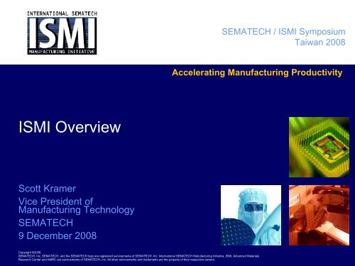
SEMATECH / <strong>ISMI</strong> Symposium<br />
Taiwan 2008<br />
Accelerating Manufacturing Productivity<br />
<strong>ISMI</strong> <strong>Overview</strong><br />
Scott Kramer<br />
Vice President of<br />
Manufacturing Technology<br />
SEMATECH<br />
9 December 2008<br />
Copyright ©2008<br />
SEMATECH, Inc. SEMATECH, and the SEMATECH logo are registered servicemarks of SEMATECH, Inc. International SEMATECH Manufacturing Initiative, <strong>ISMI</strong>, Advanced Materials<br />
Research Center and AMRC are servicemarks of SEMATECH, Inc. All other servicemarks and trademarks are the property of their respective owners.
What is <strong>ISMI</strong>?<br />
• Consortium<br />
– Semiconductor manufacturers<br />
– Membership organization<br />
– Subsidiary of SEMATECH<br />
• Cooperative work to:<br />
– Increase productivity<br />
– Decrease cost<br />
• Staffing<br />
– 50% employees<br />
– 50% assignees from member companies<br />
2
<strong>ISMI</strong> Mission<br />
<strong>ISMI</strong> provides productivity solutions for current and future<br />
challenges in the manufacturing plants of our membership,<br />
so that our members will achieve best in class productivity<br />
levels.<br />
We will accomplish this by providing platforms for<br />
collaboration among our members and directing development<br />
activities in key areas identified by our members.<br />
Accelerating Manufacturing Productivity<br />
3
What Does <strong>ISMI</strong> Do For Members?<br />
• The Productivity Challenge<br />
– How to achieve and maintain world class fab<br />
productivity<br />
– How to solve both today’s productivity problems and<br />
tomorrow’s<br />
• The Cost Reduction Challenge<br />
– How to continuously reduce costs in today’s fabs<br />
– How to manage ever increasing capital, manufacturing,<br />
and R&D costs<br />
4
<strong>ISMI</strong> Membership<br />
5
2008 <strong>ISMI</strong> Programs<br />
• An extensive set of 30 projects in 6 programs – focus on<br />
increasing productivity and decreasing cost<br />
Metrology<br />
Program<br />
ESH – Energy<br />
Savings<br />
Program<br />
<strong>ISMI</strong><br />
Councils<br />
Continuous<br />
Improvement<br />
Program<br />
Next<br />
Generation<br />
Factory<br />
Program<br />
450mm<br />
Transition<br />
Program<br />
Defect Metrology<br />
Lithography<br />
Metrology<br />
Films<br />
Metrology<br />
ESH Global<br />
Strategies<br />
ESH Resource<br />
Conservation<br />
ESH Technology<br />
Operations<br />
Councils<br />
Business<br />
Councils<br />
Productivity<br />
Workshops<br />
200mm/300mm<br />
EPITs<br />
First Wafer Delay<br />
NPW Reduction<br />
Tool Installation<br />
Factory for<br />
Small Lot Size<br />
Equipment<br />
Chamber<br />
Matching<br />
e-Manufacturing<br />
(EDA, PPM,<br />
Data Quality,<br />
Virtual<br />
Metrology)<br />
Silicon<br />
Readiness<br />
Standards and<br />
Guidelines<br />
Automation<br />
Test Bed<br />
6
<strong>ISMI</strong>: An International Consortium<br />
• Companies<br />
– 17 semiconductor member companies<br />
– Headquarters and fabs in all regions – Asia, Europe,<br />
USA<br />
• Multi-cultural environment<br />
– 14 languages<br />
– English as second language for 40% of staff<br />
7
Drive for Higher Productivity<br />
• Member companies all agree – higher productivity is a<br />
must, always<br />
• There are multiple solutions possible<br />
• <strong>ISMI</strong> philosophy – accelerate productivity improvement<br />
– Be impatient<br />
– Do not delay or hesitate<br />
– Consider all information and possible solutions<br />
8
Councils = Value = Benchmarking<br />
Activity<br />
• Benchmark metrics<br />
• Identify best-in-class<br />
• Share best practices<br />
• Site visits (fab tours)<br />
• Networking<br />
• Validate industry Roadmap direction<br />
• Communicate consensus<br />
requirements to suppliers<br />
• Sub-teams/focus groups on<br />
specific topics of interest<br />
• Organize and sponsor workshops<br />
<strong>ISMI</strong> Council Members<br />
Leave Meetings Knowing<br />
• Where their fabs rank<br />
• How to achieve world<br />
class performance<br />
• The look of a world<br />
class operation and<br />
who to talk to about it<br />
9
<strong>ISMI</strong> Councils Portfolio<br />
Manufacturing<br />
Methods Council<br />
Facilities<br />
Council<br />
Wafer Probe<br />
Council<br />
Operations<br />
Councils<br />
Yield<br />
Council<br />
Test<br />
Council<br />
Critical<br />
Materials Council<br />
Reliability<br />
Council<br />
Supplier Relations<br />
Action Council<br />
Business<br />
Councils<br />
Statistics<br />
Council<br />
Failure Analysis<br />
(FA) Council<br />
Quality<br />
Council<br />
Semiconductor<br />
Logistics Forum<br />
10
Manufacturing Methods Council<br />
Quarterly Fab Metrics<br />
Average Wafer Line Yield Per 20 Layers<br />
Quarterly Maximum<br />
Trend Data<br />
From Fab “A”<br />
Yield<br />
Median<br />
Quarterly Minimum<br />
Quarter<br />
11
300mm Fab Energy Use<br />
12
Benchmark Survey of Assembly and<br />
Test Sites - Electricity Use Example<br />
Energy usage normalized by production area<br />
kW/square meter production area<br />
1.00<br />
0.90<br />
0.80<br />
0.70<br />
0.60<br />
0.50<br />
0.40<br />
0.30<br />
0.20<br />
0.10<br />
0.00<br />
0.00 0.00<br />
More<br />
Efficient<br />
0.14 0.18 0.34<br />
Average:<br />
0.57<br />
0.46<br />
0.55<br />
0.63 0.65 0.71<br />
0.76 0.77 0.77<br />
L M A E C D J F H G N I B K<br />
Fab Letter<br />
0.91<br />
13
Example Topics from Recent<br />
Yield Council Meetings<br />
• Low Yielding Wafers:<br />
– How to characterize and disposition low yielding wafers?<br />
– Effect of development phase (R&D, ramp, production)?<br />
• Automatic Defect Classification (ADC):<br />
– How used?<br />
– What are the major issues?<br />
– Future strategy for this tool?<br />
• Defect Inspection, Identification:<br />
– Killer defect sourcing (to specific process step); e.g., particles<br />
causing metal extras<br />
– Partitioning, split experiments, any new ideas?<br />
<strong>ISMI</strong> Confidential<br />
14
Non-Product Wafer Reduction -<br />
Downgrade Procedure Analysis<br />
Particle Monitor<br />
• Process area start<br />
wafer type (prime<br />
test, product,<br />
reclaimed wafer)<br />
• Downgrade<br />
specification limits<br />
• Number of<br />
downgrades used<br />
• Downgrade flows<br />
• Best practices<br />
• Cost reduction<br />
opportunities<br />
Particle Monitor<br />
Etch rate<br />
Dummy<br />
Particle Monitor<br />
Etch rate<br />
Dummy<br />
Particle Monitor<br />
Dummy<br />
Dummy<br />
Particle Monitor<br />
Thickness<br />
Particle Monitor<br />
Thickness<br />
Dummy<br />
na<br />
Particle Monitor<br />
Thickness<br />
Dummy<br />
(Etch rate)<br />
Particle Monitor<br />
Thickness<br />
Dummy<br />
Dummy<br />
Downgrade flows<br />
15
Equipment Chamber Matching<br />
Probe yield<br />
. .<br />
.。。 . 。<br />
.. .<br />
。 。。。 。<br />
.。。 。。<br />
。<br />
.<br />
Eq1 & Eq2<br />
. Eq3<br />
t<br />
Discovery of a rogue<br />
and champion chamber<br />
Probe yield<br />
Parameter n<br />
Parameter n<br />
Eq1 Eq2 Eq3<br />
Parameter n<br />
Eq3<br />
t<br />
Discovery of a rogue parameter<br />
16
Equipment Installation Project<br />
Adapter Plate Concept<br />
3) Roll-in tool & connect<br />
4) If necessary, disconnect to<br />
move to another location<br />
5) Move equipment<br />
to another<br />
location with an<br />
awaiting adapter<br />
plate<br />
1) Install adapter plate<br />
Fab Floor<br />
2) Connect facilities<br />
17
Next Generation Factory Vision<br />
Realization<br />
• 450mm strategy - built on coordinated improvements<br />
between 300mm Prime and 450mm<br />
• Collaboration - critical success factor<br />
450mm-only<br />
450mm Readiness<br />
450 Factory Integration<br />
Test Bed<br />
450 Factory Integration<br />
Guidelines & Standards<br />
450 Silicon Wafer<br />
300mm Prime<br />
Software Infrastructure<br />
SWP/Small Lot-size Factory<br />
Availability Improvement<br />
FWD/Set-up Reduction<br />
300mm Classic<br />
Foundation<br />
18
Summary<br />
• <strong>ISMI</strong> = value for members<br />
– From leading edge to mature fabs<br />
– Focus<br />
• Productivity increase<br />
• Cost decrease<br />
• <strong>ISMI</strong> has international membership and staffing<br />
• Collaboration - world’s leading semiconductor<br />
manufacturers<br />
19
Accelerating Manufacturing Productivity<br />
Thank You!<br />
Welcome!<br />
Copyright ©2008<br />
SEMATECH, Inc. SEMATECH, and the SEMATECH logo are registered servicemarks of SEMATECH, Inc. International SEMATECH Manufacturing Initiative, <strong>ISMI</strong>, Advanced Materials<br />
Research Center and AMRC are servicemarks of SEMATECH, Inc. All other servicemarks and trademarks are the property of their respective owners.


