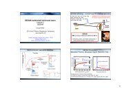
2.1 Ultrafast solid-state lasers - ETH - the Keller Group
2.1 Ultrafast solid-state lasers - ETH - the Keller Group
2.1 Ultrafast solid-state lasers - ETH - the Keller Group

Create successful ePaper yourself
Turn your PDF publications into a flip-book with our unique Google optimized e-Paper software.
86 <strong>2.1</strong>.4 Loss modulation [Ref. p. 134<br />
Beam Epitaxy (MBE) or with Metal-Organic chemical Vapor deposition (MOVPE). MBE gives us<br />
<strong>the</strong> additional flexibility to grow semiconductors at lower temperatures, down to ≈ 200 ◦ C, while<br />
MOVPE usually requires growth temperatures of ≈ 600 ◦ C to break up <strong>the</strong> incident molecules on<br />
<strong>the</strong> wafer surface during <strong>the</strong> growth. Lower growth temperatures lead to microscopic structural<br />
defects which act as traps for excited carriers and thus reduce <strong>the</strong> recovery time, which is beneficial<br />
for <strong>the</strong> use in ultrafast <strong>lasers</strong>. Optimized materials combine an ultrafast recovery time with low<br />
saturation fluence, high modulation and small nonsaturable losses. This material optimization issue<br />
has been addressed for ion-implanted [99Led] and LT-grown [96Sie, 99Hai1, 99Hai2] semiconductor<br />
saturable absorbers.<br />
<strong>2.1</strong>.4.3.3 Semiconductor saturable absorber materials<br />
Semiconductor materials offer a wide flexibility in choosing <strong>the</strong> emission wavelength of <strong>the</strong> <strong>lasers</strong>.<br />
It ranges from ≈ 400 nm in <strong>the</strong> UV using GaN-based materials to ≈ 2.5 μm in <strong>the</strong> mid-infrared using<br />
GaInAsSb-based materials. More standard high-performance semiconductor material systems<br />
which can be grown today cover <strong>the</strong> infrared wavelength range from 800 nm up to 1.5 μm. Semiconductor<br />
compounds used for <strong>the</strong>se wavelengths are AlGaAs (800 nm to 870 nm), InGaAs (870 nm to<br />
about 1150 nm), GaInNAs (1.1 μm to1.5μm), or InGaAsP (1.5-μm range). A larger wavelength<br />
range for a given material composition may only be obtained at <strong>the</strong> expense of increased defect<br />
concentrations because of an increased lattice mismatch to a given substrate material. Generally,<br />
bulk quantum-well and quantum-dot semiconductor saturable absorbers have been used. Especially,<br />
<strong>the</strong> quantum-dot saturable absorbers turned out to be advantageous for <strong>the</strong> integration into<br />
<strong>the</strong> VECSEL structure [04Lor, 07Maa].<br />
<strong>2.1</strong>.4.3.3.1 InGaAs/GaAs/AlGaAs semiconductor material system<br />
This material is best-suited for <strong>the</strong> 800 nm–1.1 μm wavelength range because of <strong>the</strong> near-perfect<br />
lattice match between GaAs and AlGaAs. InGaAs saturable absorbers have been grown on<br />
AlAs/GaAs Bragg mirrors and have been <strong>the</strong> material of choice for SESAMs at an operation<br />
wavelength of ≈ 1 μm. However, thicker InGaAs saturable absorbers above <strong>the</strong> critical thickness<br />
had surface striations that introduced too much scattering losses to be used inside a laser [94Kel].<br />
Low-temperature MBE growth (see more details in Sect. <strong>2.1</strong>.4.3.2) resulted in strain-relaxed structures<br />
with surfaces that were optically flat, but with strongly increased defect densities. For SESAM<br />
applications this is actually advantageous, and has been exploited to optimize <strong>the</strong> dynamic response<br />
of <strong>the</strong> SESAM. InGaAs saturable absorbers on AlAs/GaAs Bragg mirrors have even been used at<br />
an operation wavelength of 1.3 μm [96Flu2, 97Flu] and 1.55 μm [03Spu, 04Zel]. However, <strong>the</strong>se<br />
highly strained layers with high indium content exceed <strong>the</strong> critical thickness, and show significant<br />
nonsaturable losses due to strain and defect formation. Optimized low-temperature MBE growth,<br />
however, (Sect. <strong>2.1</strong>.4.3.2) allowed improved InGaAs SESAMs to support stable mode-locking and<br />
Q-switching in diode-pumped <strong>solid</strong>-<strong>state</strong> <strong>lasers</strong>.<br />
<strong>2.1</strong>.4.3.3.2 GaInAsP/InP semiconductor material system<br />
This material system can be lattice-matched on <strong>the</strong> InP substrate but suffers from low refractiveindex<br />
contrast and poor temperature characteristics. Due to <strong>the</strong> low refractive-index contrast,<br />
a high number of InP/GaInAsP mirror pairs are required to form Distributed Bragg Reflectors<br />
(DBRs). This demands very precise control of <strong>the</strong> growth to achieve DBRs with uniform and<br />
accurate layer thickness.<br />
Landolt-Börnstein<br />
New Series VIII/1B1