2.1 Ultrafast solid-state lasers - ETH - the Keller Group
2.1 Ultrafast solid-state lasers - ETH - the Keller Group
2.1 Ultrafast solid-state lasers - ETH - the Keller Group

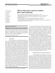
Create successful ePaper yourself
Turn your PDF publications into a flip-book with our unique Google optimized e-Paper software.
84 <strong>2.1</strong>.4 Loss modulation [Ref. p. 134<br />
Energy E<br />
e<br />
<br />
III<br />
phonon<br />
e<br />
<br />
II<br />
e<br />
IV<br />
I<br />
Wave vector<br />
k<br />
Fig. <strong>2.1</strong>.10. Schematic dispersion diagram of a 2-band bulk semiconductor<br />
showing <strong>the</strong> time regimes I–IV after optical excitation,<br />
see text for more details. e–e: electron–electron scattering.<br />
e–phonon: electron–phonon scattering.<br />
After <strong>the</strong> loss of coherence, ultrafast spectroscopy of semiconductors is solely concerned with<br />
<strong>the</strong> dynamics of <strong>the</strong> population, i.e., electron and hole distributions. In this incoherent regime,<br />
<strong>the</strong> time regimes II–IV in Fig. <strong>2.1</strong>.10 can be distinguished, as described as follows. The initial<br />
electron and hole distributions are non-<strong>the</strong>rmal in most cases, i.e., <strong>the</strong>y cannot be described by<br />
Fermi–Dirac statistics with a well-defined temperature [85Oud, 86Kno, 87Sch]. Scattering among<br />
charge carriers is mainly responsible for <strong>the</strong> redistribution of energy within <strong>the</strong> carrier distributions<br />
and for <strong>the</strong> formation of <strong>the</strong>rmal distributions. This <strong>the</strong>rmalization is shown as time regime II in<br />
Fig. <strong>2.1</strong>.10, for <strong>the</strong> example of a <strong>the</strong>rmalizing electron distribution where <strong>the</strong>rmalization occurs<br />
through scattering among <strong>the</strong> electrons. For excitation of <strong>the</strong> continuum, <strong>the</strong>rmalization usually<br />
occurs on a time scale of 100 fs under most experimental conditions. The exact <strong>the</strong>rmalization time<br />
strongly depends on <strong>the</strong> carrier density, <strong>the</strong> excess photon energy with respect to <strong>the</strong> band edge<br />
and <strong>the</strong> type of carrier [99Sha].<br />
In general, <strong>the</strong> carriers have a temperature different from <strong>the</strong> lattice temperature after <strong>the</strong>rmalization<br />
has been completed. In Fig. <strong>2.1</strong>.10 it is assumed that <strong>the</strong> carriers have a higher temperature<br />
than <strong>the</strong> lattice. For this case, Fig. <strong>2.1</strong>.10 schematically shows <strong>the</strong> cooling of carriers by <strong>the</strong> emission<br />
of phonons, i.e., energy transfer to <strong>the</strong> lattice. Cooling defines <strong>the</strong> time regime III. Typical<br />
time constants are in <strong>the</strong> picosecond and tens of picosecond range.<br />
Finally, <strong>the</strong> optically excited semiconductor returns to <strong>the</strong>rmodynamic equilibrium by <strong>the</strong> recombination<br />
of electron–hole pairs. Recombination is shown as time regime IV in Fig. <strong>2.1</strong>.10. In a<br />
perfect semiconductor crystal, recombination proceeds via <strong>the</strong> emission of photons or Auger processes<br />
at high carrier densities. These recombination processes in a good quality semiconductor<br />
(i.e. with a low level of defect <strong>state</strong>s) take place on time scales of hundreds of picoseconds and<br />
longer.<br />
Ano<strong>the</strong>r ultrafast process is encountered if large densities of deep-level traps are incorporated<br />
in a semiconductor. Trapping of carriers into deep levels can proceed on sub-picosecond time<br />
scales (not shown in Fig. <strong>2.1</strong>.10). Since carrier trapping is important in many saturable absorber<br />
applications, it is discussed in more details in Sect. <strong>2.1</strong>.4.3.2.<br />
We note that <strong>the</strong> different time regimes temporally overlap. For example, a scattering process<br />
may destroy <strong>the</strong> coherence and contribute to <strong>the</strong>rmalization. Never<strong>the</strong>less, it is very useful to<br />
distinguish between <strong>the</strong> different time regimes because <strong>the</strong>y are a convenient means for <strong>the</strong> description<br />
of <strong>the</strong> complex semiconductor dynamics. The schematic picture of <strong>the</strong> different time regimes<br />
also demonstrates that two or more time constants are usually required to describe <strong>the</strong> temporal<br />
response of a semiconductor absorber. For example, we recall that <strong>the</strong>rmalization typically takes<br />
place on <strong>the</strong> 100-fs time scale while carrier trapping proceeds on time scales from a few hundreds<br />
Landolt-Börnstein<br />
New Series VIII/1B1