
Create successful ePaper yourself
Turn your PDF publications into a flip-book with our unique Google optimized e-Paper software.
SEQUENTIAL CIRCUITS<br />
http://www.tuto rialspo int.co m/co mputer_lo g ical_o rg aniz atio n/sequential_circuits.htm<br />
Copyrig ht © tutorialspoint.com<br />
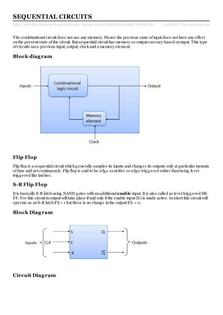
The combinational circuit does not use any memory. Hence the previous state of input does not have any effect<br />
on the present state of the circuit. But sequential circuit has memory so output can vary based on input. This type<br />
of circuits uses previous input, output, clock and a memory element.<br />
Block diag ram<br />
Flip Flop<br />
Flip flop is a sequential circuit which g enerally samples its inputs and chang es its outputs only at particular instants<br />
of time and not continuously. Flip flop is said to be edg e sensitive or edg e trig g ered rather than being level<br />
trig g ered like latches.<br />
S-R Flip Flop<br />
It is basically S-R latch using NAND g ates with an additional enable input. It is also called as level trig g ered SR-<br />
FF. For this circuit in output will take place if and only if the enable input (E) is made active. In short this circuit will<br />
operate as an S-R latch if E= 1 but there is no chang e in the output if E = 0.<br />
Block Diag ram<br />
Circuit Diag ram
Truth Table<br />
Operation<br />
S.N. Condition Operation<br />
1 S = R = 0 : No<br />
chang e If S = R = 0 then output of NAND g ates 3 and 4 are forced to become 1.<br />
Hence R' and S' both will be equal to 1. Since S' and R' are the input of the<br />
basic S-R latch using NAND g ates, there will be no chang e in the state of<br />
outputs.<br />
2 S = 0, R = 1, E =<br />
1 Since S = 0, output of NAND-3 i.e. R' = 1 and E = 1 the output of NAND-<br />
4 i.e. S' = 0.<br />
Hence Q n+1 = 0 and Q n+1 bar = 1. This is reset condition.<br />
3 S = 1, R = 0, E =<br />
1 Output of NAND-3 i.e. R' = 0 and output of NAND-4 i.e. S' = 1.<br />
Hence output of S-R NAND latch is Q n+1 = 1 and Q n+1 bar = 0. This is<br />
the reset condition.<br />
4 S = 1, R = 1, E =<br />
1 As S = 1, R = 1 and E = 1, the output of NAND g ates 3 and 4 both are 0<br />
i.e. S' = R' = 0.<br />
Hence the Race condition will occur in the basic NAND latch.
Master Slave JK Flip Flop<br />
Master slave JK FF is a cascade of two S-R FF with feedback from the output of second to input of first. Master<br />
is a positive level trig g ered. But due to the presence of the inverter in the clock line, the slave will respond to the<br />
neg ative level. Hence when the clock = 1 (positive level) the master is active and the slave is inactive. Whereas<br />
when clock = 0 (low level) the slave is active and master is inactive.<br />
Circuit Diag ram<br />
Truth Table<br />
Operation<br />
S.N. Condition Operation<br />
1 J = K = 0 (No<br />
chang e)<br />
When clock = 0, the slave becomes active and master is inactive. But<br />
since the S and R inputs have not chang ed, the slave outputs will also<br />
remain unchang ed. Therefore outputs will not chang e if J = K =0.<br />
2 J = 0 and K = 1<br />
(Reset)<br />
Clock = 1: Master active, slave inactive. Therefore outputs of the master<br />
become Q 1 = 0 and Q 1 bar = 1. That means S = 0 and R =1.<br />
Clock = 0: Slave active, master inactive Therefore outputs of the slave<br />
become Q = 0 and Q bar = 1.<br />
Ag ain clock = 1: Master active, slave inactive. Therefore even with the<br />
chang ed outputs Q = 0 and Q bar = 1 fed back to master, its outputs will<br />
Q1 = 0 and Q1 bar = 1. That means S = 0 and R = 1.
Hence with clock = 0 and slave becoming active the outputs of slave will<br />
remain Q = 0 and Q bar = 1. Thus we g et a stable output from the<br />
Master slave.<br />
3 J = 1 and K = 0<br />
(Set)<br />
Clock = 1: Master active, slave inactive. Therefore outputs of the master<br />
become Q 1 = 1 and Q 1 bar = 0. That means S = 1 and R =0.<br />
Clock = 0: Slave active, master inactive Therefore outputs of the slave<br />
become Q = 1 and Q bar = 0.<br />
Ag ain clock = 1: then it can be shown that the outputs of the slave are<br />
stabilized to Q = 1 and Q bar = 0.<br />
4 J = K = 1<br />
(Tog g le)<br />
Clock = 1: Master active, slave inactive. Outputs of master will tog g le.<br />
So S and R also will be inverted.<br />
Clock = 0: Slave active, master inactive. Outputs of slave will tog g le.<br />
These chang ed output are returned back to the master inputs. But since<br />
clock = 0, the master is still inactive. So it does not respond to these<br />
chang ed outputs. This avoids the multiple tog g ling which leads to the<br />
race around condition. The master slave flip flop will avoid the race<br />
around condition.<br />
Delay Flip Flop / D Flip Flop<br />
Delay Flip Flop or D Flip Flop is the simple g ated S-R latch with a NAND inverter connected between S and R<br />
inputs. It has only one input. The input data is appearing at the output after some time. Due to this data delay<br />
between i/p and o/p, it is called delay flip flop. S and R will be the complements of each other due to NAND<br />
inverter. Hence S = R = 0 or S = R = 1,these input condition will never appear. This problem is avoid by SR = 00<br />
and SR = 1 conditions.<br />
Block Diag ram<br />
Circuit Diag ram
Truth Table<br />
Operation<br />
S.N. Condition Operation<br />
1 E = 0<br />
Latch is disabled. Hence is no chang e in output.<br />
2 E = 1 and D = 0<br />
If E = 1 and D = 0 then S = 0 and R = 1. Hence irrespective of the<br />
present state, the next state is Q n+1 = 0 and Q n+1 bar = 1. This is the<br />
reset condition.<br />
3 E = 1 and D = 1<br />
if E = 1 and D = 1, then S = 1 and R = 0. This will set the latch and Q n+1 = 1<br />
and Q n+1 bar = 0 irrespective of the present state.<br />
Tog g le Flip Flop / T Flip Flop<br />
Tog g le flip flop is basically a JK flip flop with J and K terminals permanently connected tog ether. It has only input<br />
denoted by T is shown in the Symbol Diag ram. The symbol for positive edg e trig g ered T flip flop is shown in the<br />
Block Diag ram.<br />
Symbol Diag ram
Block Diag ram<br />
Truth Table<br />
Operation<br />
S.N. Condition Operation<br />
1 T = 0, J = K = 0<br />
The output Q and Q bar won't chang e<br />
2 T = 1 ,J = K = 1<br />
output will tog g le corresponding to every leading edg e of clock sig nal.