Combinational Circuits - Tutorials Point
Combinational Circuits - Tutorials Point
Combinational Circuits - Tutorials Point

Create successful ePaper yourself
Turn your PDF publications into a flip-book with our unique Google optimized e-Paper software.
COMBINATIONAL CIRCUITS<br />
http://www.tuto rialspo int.co m/co mputer_lo g ical_o rg aniz atio n/co mbinatio nal_circuits.htm Copyrig ht © tutorialspoint.com<br />
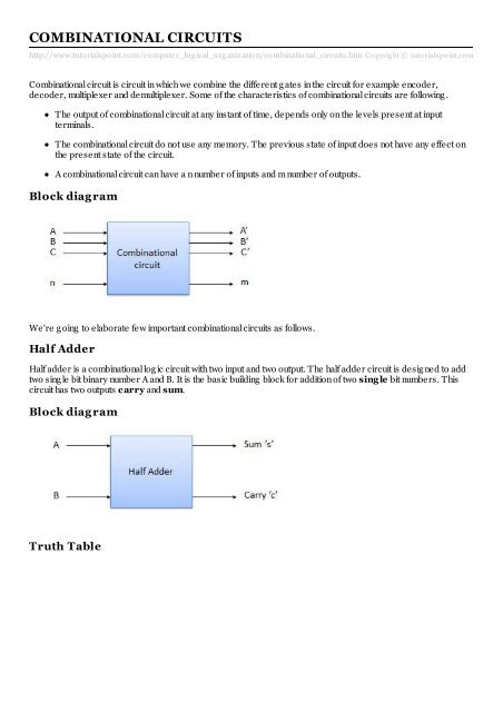
<strong>Combinational</strong> circuit is circuit in which we combine the different g ates in the circuit for example encoder,<br />
decoder, multiplexer and demultiplexer. Some of the characteristics of combinational circuits are following .<br />
The output of combinational circuit at any instant of time, depends only on the levels present at input<br />
terminals.<br />
The combinational circuit do not use any memory. The previous state of input does not have any effect on<br />
the present state of the circuit.<br />
A combinational circuit can have a n number of inputs and m number of outputs.<br />
Block diag ram<br />
We're g oing to elaborate few important combinational circuits as follows.<br />
Half Adder<br />
Half adder is a combinational log ic circuit with two input and two output. The half adder circuit is desig ned to add<br />
two sing le bit binary number A and B. It is the basic building block for addition of two sing le bit numbers. This<br />
circuit has two outputs carry and sum.<br />
Block diag ram<br />
Truth Table
Circuit Diag ram<br />
Full Adder<br />
Full adder is developed to overcome the drawback of Half Adder circuit. It can add two one-bit numbers A and B,<br />
and carry c. The full adder is a three input and two output combinational circuit.<br />
Block diag ram<br />
Truth Table
Circuit Diag ram<br />
N-Bit Parallel Adder<br />
The Full Adder is capable of adding only two sing le dig it binary number along with a carry input. But in practical<br />
we need to add binary numbers which are much long er than just one bit. To add two n-bit binary numbers we<br />
need to use the n-bit parallel adder. It uses a number of full adders in cascade. The carry output of the previous<br />
full adder is connected to carry input of the next full adder.<br />
4 Bit Parallel Adder<br />
In the block diag ram, A 0 and B 0 represent the LSB of the four bit words A and B. Hence Full Adder-0 is the<br />
lowest stag e. Hence its C in has been permanently made 0. The rest of the connections are exactly same as<br />
those of n-bit parallel adder is shown in fig . The four bit parallel adder is a very common log ic circuit.<br />
Block diag ram
N-Bit Parallel Subtractor<br />
The subtraction can be carried out by taking the 1's or 2's complement of the number to be subtracted. For<br />
example we can perform the subtraction (A-B) by adding either 1's or 2's complement of B to A. That means we<br />
can use a binary adder to perform the binary subtraction.<br />
4 Bit Parallel Subtractor<br />
The number to be subtracted (B) is first passed throug h inverters to obtain its 1's complement. The 4-bit adder<br />
then adds A and 2's complement of B to produce the subtraction. S 3 S 2 S 1 S 0 represent the result of binary<br />
subtraction (A-B) and carry output C o ut represents the polarity of the result. If A > B then Cout =0 and the result<br />
of binary form (A-B) then C o ut = 1 and the result is in the 2's complement form.<br />
Block diag ram<br />
Half Subtractors<br />
Half subtractor is a combination circuit with two inputs and two outputs (difference and borrow). It produces the<br />
difference between the two binary bits at the input and also produces a output (Borrow) to indicate if a 1 has been<br />
borrowed. In the subtraction (A-B), A is called as Minuend bit and B is called as Subtrahend bit.
orrowed. In the subtraction (A-B), A is called as Minuend bit and B is called as Subtrahend bit.<br />
Truth Table<br />
Circuit Diag ram<br />
Full Subtractors<br />
The disadvantag e of a half subtractor is overcome by full subtractor. The full subtractor is a combinational circuit<br />
with three inputs A,B,C and two output D and C'. A is the minuend, B is subtrahend, C is the borrow produced by<br />
the previous stag e, D is the difference output and C' is the borrow output.<br />
Truth Table<br />
Circuit Diag ram
Multiplexers<br />
Multiplexer is a special type of combinational circuit. There are n-data inputs, one output and m select inputs with<br />
2m = n. It is a dig ital circuit which selects one of the n data inputs and routes it to the output. The selection of one<br />
of the n inputs is done by the selected inputs. Depending on the dig ital code applied at the selected inputs, one<br />
out of n data sources is selected and transmitted to the sing le output Y. E is called the strobe or enable input<br />
which is useful for the cascading . It is g enerally an active low terminal, that means it will perform the required<br />
operation when it is low.<br />
Block diag ram<br />
Multiplexers come in multiple variations<br />
2 : 1 multiplexer
4 : 1 multiplexer<br />
16 : 1 multiplexer<br />
32 : 1 multiplexer<br />
Block Diag ram<br />
Truth Table<br />
Demultiplexers<br />
A demultiplexer performs the reverse operation of a multiplexer i.e. it receives one input and distributes it over<br />
several outputs. It has only one input, n outputs, m select input. At a time only one output line is selected by the<br />
select lines and the input is transmitted to the selected output line. A de-multiplexer is equivalent to a sing le pole<br />
multiple way switch as shown in fig .<br />
Demultiplexers come in multiple variations<br />
1 : 2 demultiplexer<br />
1 : 4 demultiplexer<br />
1 : 16 demultiplexer<br />
1 : 32 demultiplexer<br />
Block diag ram
Truth Table<br />
Decoder<br />
A decoder is a combinational circuit. It has n input and to a maximum m = 2n outputs. Decoder is identical to a<br />
demultiplexer without any data input. It performs operations which are exactly opposite to those of an encoder.<br />
Block diag ram<br />
Examples of Decoders are following .<br />
Code converters<br />
BCD to seven seg ment decoders<br />
Nixie tube decoders<br />
Relay actuator<br />
2 to 4 Line Decoder<br />
The block diag ram of 2 to 4 line decoder is shown in the fig . A and B are the two inputs where D throug h D are<br />
the four outputs. Truth table explains the operations of a decoder. It shows that each output is 1 for only a specific<br />
combination of inputs.<br />
Block diag ram
Truth Table<br />
Log ic Circuit<br />
Encoder<br />
Encoder is a combinational circuit which is desig ned to perform the inverse operation of the decoder. An<br />
encoder has n number of input lines and m number of output lines. An encoder produces an m bit binary code<br />
corresponding to the dig ital input number. The encoder accepts an n input dig ital word and converts it into an m<br />
bit another dig ital word.
Block diag ram<br />
Examples of Encoders are following .<br />
Priority encoders<br />
Decimal to BCD encoder<br />
Octal to binary encoder<br />
Hexadecimal to binary encoder<br />
Priority Encoder<br />
This is a special type of encoder. Priority is g iven to the input lines. If two or more input line are 1 at the same<br />
time, then the input line with hig hest priority will be considered. There are four input D 0 , D 1 , D 2 , D 3 and two<br />
output Y 0 , Y 1 . Out of the four input D 3 has the hig hest priority and D 0 has the lowest priority. That means if D 3 = 1<br />
then Y 1 Y 1 = 11 irrespective of the other inputs. Similarly if D 3 = 0 and D 2 = 1 then Y 1 Y 0 = 10 irrespective of the<br />
other inputs.<br />
Block diag ram<br />
Truth Table
Log ic Circuit