FNA Annual Report 2010 - Technische Universiteit Eindhoven
FNA Annual Report 2010 - Technische Universiteit Eindhoven
FNA Annual Report 2010 - Technische Universiteit Eindhoven

Create successful ePaper yourself
Turn your PDF publications into a flip-book with our unique Google optimized e-Paper software.
TU e<br />
<strong>Technische</strong><br />
<strong>Universiteit</strong><br />
<strong>Eindhoven</strong><br />
University of Technology<br />
Group Physics of Nanostructures<br />
Department of Applied Physics<br />
Group Physics of Nanostructures<br />
Department of Applied Physics<br />
TU/e<br />
<strong>Technische</strong><br />
<strong>Universiteit</strong><br />
<strong>Eindhoven</strong><br />
University of Technology<br />
<strong>Annual</strong> <strong>Report</strong><br />
<strong>2010</strong><br />
Where innovation starts
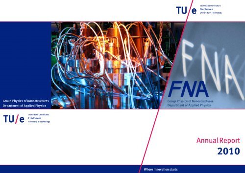
<strong>Annual</strong> <strong>Report</strong> <strong>2010</strong><br />
Physics of Nanostructures group (<strong>FNA</strong>)<br />
Department of Applied Physics<br />
<strong>Eindhoven</strong> University of Technology<br />
Physics of Nanostructures<br />
NLe 1.06<br />
Den Dolech 2<br />
P.O. Box 513<br />
5600 MB <strong>Eindhoven</strong><br />
The Netherlands<br />
Tel.: 040 2475778<br />
Fax: 040 2475724<br />
E-mail: c.a.m.jansen@tue.nl<br />
Website: http://www.fna.phys.tue.nl
2 <strong>FNA</strong> <strong>Annual</strong> <strong>Report</strong> <strong>2010</strong> 0.Table of Contents<br />
Editors:<br />
M. Hoeijmakers BSc.<br />
T. Weekenstroo BSc.
<strong>FNA</strong> <strong>Annual</strong> <strong>Report</strong> <strong>2010</strong> 0.Table of Contents 3<br />
Table of Contents<br />
1 Introduction....................................................................................................................................... 4<br />
2 Acknowledgments ........................................................................................................................... 7<br />
3 Group Members ............................................................................................................................... 9<br />
3.1 List of Group Members ...................................................................................................................... 9<br />
3.2 Photos of Group Members ............................................................................................................... 11<br />
3.3 Group Photo ....................................................................................................................................... 12<br />
4 Equipment ....................................................................................................................................... 13<br />
4.1 EUFORAC deposition and in-situ analysis facility ...................................................................... 13<br />
4.2 Scanning Probe Microscopy and Laser laboratories .................................................................... 14<br />
4.3 Ex-situ structural, electrical, and magnetic characterization ...................................................... 16<br />
4.4 Nanostructuring ................................................................................................................................ 17<br />
5 Research Projects ............................................................................................................................ 19<br />
5.1 NanoMagnetism ................................................................................................................................ 19<br />
5.2 Spintronics .......................................................................................................................................... 20<br />
5.3 Ultrafast spin dynamics .................................................................................................................... 21<br />
6 Results .............................................................................................................................................. 23<br />
6.1 Nano Magnetism ............................................................................................................................... 24<br />
6.2 Spintronics .......................................................................................................................................... 34<br />
6.3 Ultrafast Spin Dynamics ................................................................................................................... 48<br />
7 Output .............................................................................................................................................. 61<br />
7.1 Publications ........................................................................................................................................ 61<br />
7.2 Presentations ...................................................................................................................................... 62<br />
7.3 Chapters .............................................................................................................................................. 65<br />
7.4 Guest Lectures ................................................................................................................................... 66<br />
7.5 Posters ................................................................................................................................................. 66<br />
7.6 PhD Theses ......................................................................................................................................... 67<br />
7.7 Master Theses..................................................................................................................................... 67<br />
7.8 Internship <strong>Report</strong>s ............................................................................................................................. 68<br />
7.9 Publicity .............................................................................................................................................. 69<br />
8 Social Events ................................................................................................................................... 75
4 <strong>FNA</strong> <strong>Annual</strong> <strong>Report</strong> <strong>2010</strong> 0.Table of Contents
<strong>FNA</strong> <strong>Annual</strong> <strong>Report</strong> <strong>2010</strong> 1.Introduction 5<br />
1 Introduction<br />
Dear colleagues and friends of <strong>FNA</strong>,<br />
This <strong>Annual</strong> report of our group Physics of Nanostructures (<strong>FNA</strong>) at the <strong>Eindhoven</strong> University of Technology<br />
covers facts & figures as well as highlights of the year <strong>2010</strong>. In particular it provides a review over research<br />
progress in the fields we are active in, viz. nanomagnetism, spin-polarized transport and ultrafast magnetic<br />
processes. It has become a tradition that two of our master students take the lead in the editorial process – while<br />
all group members contribute to the contents. With the final results we hope to present you an overview of not<br />
only our scientific achievements, but also providing you a glimpse of the atmosphere in our group.<br />
Within the department of Applied Physics, the past year was a special one in which we celebrated our 50 th<br />
anniversary. Many activities were organized, such as a grand party for all members and students of the<br />
department, and an ‘open day’ to which many of our group members contributed. It attracted a large number of<br />
visitors from all ages to our department. Nano-quizzes in which enthusiastic kids were confronted with the<br />
amazing world of nanotechnology, demos of our electromagnetic launching-gear (‘coil-gun’) – shooting quite a<br />
few trays with high precision, and a nano-slide show accompanied by a 3 byte-harddisk demo where young<br />
kids took care of ultimate spinning speeds. Finally, the main star was our EUFORAC (<strong>Eindhoven</strong> University<br />
nano-Film depOsition Research and Analysis System). Lighted by disco lights (see cover) the audience was<br />
enjoying explanations about atom-by-atom deposition and its applications in spintronics.<br />
The year <strong>2010</strong> was also a year of several lively international meetings organized by the group. End of June we<br />
hosted the joint Dutch-Korean meeting on Spintronics. The lectures in the Guus Hiddink hall, and a trip to the<br />
catacombs of the PSV-stadium (where quite a few Korean players were starring at the exhibitions), may have<br />
been particularly memorable for our guests. Early September, we organized (co-chaired by Peter Bobbert from<br />
our partner group at the department) the 3 rd International Conference on Spins in Organic Semiconductors in<br />
the historical Trippenhuis along the canals in downtown Amsterdam. The conference marked the end of the<br />
first phase of our Vici-program on organic spintronics. It attracted a record number of participants from all over<br />
the world, and illustrated the enormous development in the new field of research – combining issues in<br />
spintronics and organic electronics.<br />
As to scientific progress, the year <strong>2010</strong> showed new exciting results in fields of research we are traditionally<br />
strong in over the past years, but also important breakthroughs in new areas. Here, in particular, I want to<br />
mention our work in domain wall motion, and first successes in writing truly ferromagnetic nanostructures<br />
using our focused electron-beam induced nano-pencil. Thus, students produced our group’s logo with a 300 nm<br />
wide font of free standing ferromagnetic letters (see cover); results obtained in intense collaboration with FEI<br />
company. Among other new research programs, the national FOM program on ‘Controlling Spin Dynamics in<br />
Magnetic Nanostructures’ got a real start, our collaboration with Hitachi Global Storage Technologies (San Jose,<br />
CA) got formalized in the framework of a joint research effort, and our collaboration with our TU/e<br />
distinguished professor Stuart Parkin (IBM Almaden Research Center at San Jose, CA) will gain momentum<br />
again with a new PhD project. Finally, after several years of preparation, we’re particularly pleased about<br />
having obtained new funding opportunities for nano-research at TU/e within the Dutch NanoLab, and to<br />
welcome the final start-up of the new Dutch nanotechnology research program NanoNextNL. The latter is the<br />
successor of the NanoNed program, which may be familiar to some of you.<br />
Looking back the year, we saw a lot of new PhD/master/bachelor students coming and leaving the group, each<br />
of them leaving social and scientific footprints. In particular we had three PhD students getting their doctoral<br />
degree, Wiebe Wagemans, Francisco Bloom, and Reinoud Lavrijsen (early 2011) – each of them producing really<br />
high quality PhD theses and impressive publications scores. Without having the opportunity mentioning all of<br />
the other students, researchers, non-scientific staff members, as well as external collaborators, I do want to<br />
acknowledge their important contributions to our successes.
6 <strong>FNA</strong> <strong>Annual</strong> <strong>Report</strong> <strong>2010</strong> 1.Introduction<br />
Finally, the news of <strong>2010</strong>/2011 that is going to have the most significant impact on the future of the group<br />
regards our housing. Early 2011, the final decision was announced that our department will move to an entirely<br />
new building that will be constructed in the framework of the ‘Campus 2020’ project. Although beyond doubt it<br />
is something that is going to ask a lot of efforts from all our group members, it will also provide us with unique<br />
opportunities. While you are reading this <strong>Annual</strong> report, we are shaping our group’s future infrastructure. We<br />
are looking forward continuing our stimulating interaction with you also within the future setting.<br />
Best regards,<br />
Bert Koopmans
<strong>FNA</strong> <strong>Annual</strong> <strong>Report</strong> <strong>2010</strong> 2.Acknowledgments 7<br />
2 Acknowledgments<br />
Department of Applied Physics of TU/e (Peter Bobbert, René Janssen, Martijn Kemerink, Paul<br />
Koenraad, Ton van Leeuwen, Thijs Meijer, Leo van IJzendoorn, Menno Prins, Peter Nouwens)<br />
Department of Chemical engineering and Chemistry of TU/e (Martijn Wienk)<br />
Department of Electrical engineering of TU/e (Siang Oei, Erik Jan van Geluk, Barry Smalbrugge, Meint<br />
Smit, Tjibbe de Vries)<br />
AGH Krakow (Maciej Czapkiewicz, Tomasz Stobiecki)<br />
CEMES-CNRS Toulouse (Etienne Snoeck)<br />
CNRS Paris (Gregory Malinowski)<br />
FEI Company (Hans Mulders, Piet Trompenaars)<br />
FIAT Research (Daniele Pullini)<br />
Hitachi Global Storage Technologies, San Jose (Paul van der Heijden, Jeff Childress, Young-Suk Choi)<br />
Holst Centre (Herman Schoo, Jo De Boeck)<br />
IBM Almaden Research Center (Stuart Parkin, Luc Thomas)<br />
IFW Dresden (Sabine Würmehl)<br />
Indian Institute of Science Bangalore, India (Anil Kumar)<br />
Inha University (Chun-Yeol You)<br />
IMEC at Leuven (Wim Van Roy, Liesbet Lagae, Jan Genoe, Koen Weerts)<br />
ISMN-CNR Bologna (Alek Dediu)<br />
Kavli Institute of NanoScience at Delft (Emile van der Drift, Arnold van Run, Anja van Langen)<br />
Korea University (Kungwon Rhie)<br />
Kyoto University (Teruo Ono)<br />
Leeds University (Chris Marrows)<br />
LLG Micromagnetics Simulator (Mike Scheinfein)<br />
Max-Planck-Institut für metallforschung (Manfred Fähnle, Daniel Steiauf)<br />
MIT Cambridge (Jagadeesh Moodera)<br />
MESA+, University of Twente (Ron Jansen, Vishwas Gadgil)<br />
NXP (Friso Jedema, Michiel van Duuren, Fred Roozeboom)<br />
Omicron NanoTechnology GmbH (Marcus Maier, Dieter Pohlenz, Joerg Seifritz)<br />
Philips Research (Reinder Coehoorn, Hans Boeve, Menno Prins, Dago De Leeuw, Denis Markov)<br />
Polish Academy of Sciences at Warsaw (Tomasz Story, Grzegorz Karczewski)<br />
Radboud University at Nijmegen (Rob de Groot, Gilles de Wijs, Jisk Attema, Theo Rasing, Andrei<br />
Kirilyuk, Alexey Kimel)<br />
Royal Institute of Technology, Stockholm (Stefano Bonetti, Johan Åkerman)<br />
Russian Academy of Science, St. Petersburg (Yurii Vladimirovich Trushin)<br />
SmartTip Probe Solutions (Roeland Huijink, Daan Bijl)<br />
Sogang University (Myung-Hwa Jung)<br />
SPECS Nanotechnology (Ad Ettema)<br />
Tecnische Universität Dresden (Karl Leo)<br />
TNO Science and Industry, Delft (Emile van Veldhoven, Diederik Maas)<br />
University of Alabama (Patrick LeClair, Tim Mewes)<br />
University of Antwerp (Etienne Goovaerts, Hans Moons)<br />
University of Goettingen (Markus Muenzenberger)<br />
University of Iowa (Markus Wohlgenannt)<br />
University of Kaiserslautern (Burkard Hillebrands, Martin Aeschlimann, Mirko Cinchetti, Tobias Röth)<br />
University of Konstanz (Mathias Kläui, Philipp Möhrke, Ulrich Rüdiger)<br />
University of Leeds (Serban Lepadatu, Chris Marrows, Brian Hickey)<br />
University of Mainz (Claudia Felser, Gerhard Fecher, Benjamin Balke, Christian Blum)<br />
University of Zaragoza (Rosa Córdoba Castillo, José Maria De Teresa, Manuel Ricardo Ibarra García,<br />
Frank Schoenaker)<br />
Uppsala Unitversity (Björgvin Hjörvarsson)<br />
Utrecht University (Rembert Duine, Erik van der Bijl)<br />
Yacht (Veronica den Bekker-Tiba)
8 <strong>FNA</strong> <strong>Annual</strong> <strong>Report</strong> <strong>2010</strong> 2.Acknowledgments
<strong>FNA</strong> <strong>Annual</strong> <strong>Report</strong> <strong>2010</strong> 3.Group Members 9<br />
3 Group Members<br />
3.1 List of Group Members<br />
Scientific Staff<br />
Prof. dr. B. (Bert) Koopmans (group leader)<br />
Prof. dr. ir. H.J.M. (Henk) Swagten<br />
Dr. J.T. (Jürgen) Kohlhepp<br />
Dr. O. (Oleg) Kurnosikov<br />
Prof. dr. W.J.M. (Wim) de Jonge (emeritus)<br />
Guests<br />
Prof. S.S.P. (Stuart) Parkin (Distinguished professor at TU/e)<br />
Technical Staff and Operators<br />
G.W.M. (Gerrie) Baselmans<br />
Ir. J. (Jeroen) Francke<br />
Ing. J.J.P.A.W. (Jef) Noijen<br />
Dr. B. (Beatriz) Barcones Campo<br />
Secretary<br />
C.A.M. (Karin) Jansen<br />
Post-Doctoral Staff<br />
Dr. E. (Elena) Murè since 01-06-‘10<br />
Dr. D. (Daowei) Wang since 01-09-‘10<br />
PhD Students<br />
Ir. W. (Wiebe) Wagemans until 14-06-‘10<br />
F. (Francisco) Bloom MSc. until 22-11-‘10<br />
Ir. P. (Paul) Janssen<br />
Ir. K.C. (Koen) Kuiper<br />
Ir. R. (Reinoud) Lavrijsen<br />
A.J. (Sjors) Schellekens MSc. since 01-03-‘10<br />
J.H. (Jeroen) Franken MSc. since 15-03-‘10<br />
Master Students<br />
A.J. (Sjors) Schellekens until 11-02-‘10<br />
J.H. (Jeroen) Franken until 12-02-‘10<br />
F.J. (Frank) Schoenaker until 17-02-‘10<br />
C.O. (Can) Avci until 05-08-‘10<br />
M.J.M. (Mathijs) van Schijndel until 18-10-‘10<br />
R. (Rik) Paesen until 19-10-‘10<br />
P.E.D. (Paul) Soto Rodriguez MSc. until 03-11-‘10<br />
G.C.F.L. (Geerit) Kruis until 16-12-‘10<br />
T.H. (Tim) Ellis<br />
N. (Niels) de Vreede<br />
M. (Matthijs) Cox since 01-02-‘10<br />
S. (Sükrü) Hasdemir since 04-02-‘10<br />
M. (Mark) Hoeijmakers since 15-06-‘10<br />
T. (Tim) Weekenstroo since 01-09-‘10
10 <strong>FNA</strong> <strong>Annual</strong> <strong>Report</strong> <strong>2010</strong> 3.Group Members<br />
Bachelor Students<br />
M. (Mark) Herps until 26-01-‘10<br />
F.H.A. (Frank) Elich from 22-04-’10 until 11-10-‘10<br />
W. (Wouter) Verhoeven from 11-05-‘10 until 07-12-‘10<br />
Ing. C. (Christiaan) Otten since 07-09-‘10<br />
J. (Jeroen) de Groot since 11-10-‘10
<strong>FNA</strong> <strong>Annual</strong> <strong>Report</strong> <strong>2010</strong> 3.Group Members 11<br />
3.2 Photos of Group Members<br />
Beatriz Barcones Campo Gerrie Baselmans Francisco Bloom Jeroen Francke<br />
Jeroen Franken Karin Jansen Paul Janssen Wim de Jonge<br />
Jürgen Kohlhepp Bert Koopmans Koen Kuiper Oleg Kurnosikov<br />
Reinoud Lavrijsen Elena Murè Jef Noijen Henk Swagten
12 <strong>FNA</strong> <strong>Annual</strong> <strong>Report</strong> <strong>2010</strong> 3.Group Members<br />
Sjors Schellekens Wiebe Wagemans Daowei Wang<br />
3.3 Group Photo
<strong>FNA</strong> <strong>Annual</strong> <strong>Report</strong> <strong>2010</strong> 4.Equipment 13<br />
4 Equipment<br />
Research in the group Physics of Nanostructures is aimed at the engineering and investigation of functional<br />
nanostructures. Current emphasis is on structures and devices with application potential in the field of<br />
spintronics, (magnetic) data storage, and sensors. A state-of-the-art infrastructure for preparation and<br />
manipulation, as well as in-situ and ex-situ characterization of nanostructures, is available.<br />
4.1 EUFORAC deposition and in-situ analysis facility<br />
The group Physics of Nanostructures is equipped with a state-of-the-art deposition and analysis facility<br />
EUFORAC, the <strong>Eindhoven</strong> University nano-Film depOsition Research and Analysis Center.<br />
In EUFORAC a complementary cluster of ultra-high vacuum (UHV) deposition and analysis facilities are<br />
present, and exists of:<br />
<br />
<br />
<br />
<br />
<br />
<br />
<br />
MEMULA: Vacuum Generators V80 M MBE: The MEMULA (MEtallic MUltiLAyers) is a general purpose<br />
MBE for deposition of (magnetic) metallic multilayer systems. It features: a base pressure below 10 -11 mbar;<br />
7 deposition sources (4 Knudsen cells, 3 e-guns); and wedge growth and shadow mask evaporation<br />
(roughly < 50 micron resolution)<br />
CARUSO: Kurt J. Lesker UHV sputter facility: CARUSO, the Chamber for ARtificial Ultra-high vacuum<br />
Sputtered nanOstructures, is a dedicated, computer-controlled sputter coater manufactured at Kurt J.<br />
Lesker Co. Vacuum Products, and is connected to the Vacuum Generators V80 M MBE (MEMULA) as<br />
shown on the left side of the picture. The system is configured for sputter-down deposition, using oil-free<br />
diaphragm, molecular drag, and cryopumps.<br />
XPS, AES, RHEED, LEED: UHV chambers for in-situ analysis of the deposited layers with XPS, AES,<br />
RHEED, and LEED.<br />
Omicron-1 STM: A chamber for room-temperature scanning tunneling microscopy using the standard<br />
Omicron-1 system.<br />
Plasma oxidation: A chamber for DC/RF glow discharge oxidation of metal layers (such as Al), in<br />
particular to serve as a barrier in magnetic tunnel junctions. The system includes in-situ differential<br />
ellipsometry and an automized dosage system for reproducible oxidation of ultrathin films.<br />
Organic layer deposition: A UHV chamber for deposition and optical thickness control of hybrid<br />
nanostructured systems of metallic and organic materials.<br />
Glovebox: Facility for measuring (organic) samples in an oxygen and water free environment with options<br />
to measure with a modulated magnetic field and with temperatures down to 10 K.
14 <strong>FNA</strong> <strong>Annual</strong> <strong>Report</strong> <strong>2010</strong> 4.Equipment<br />
4.2 Scanning Probe Microscopy and Laser laboratories<br />
A series of inter-communicating labs for low-temperature STM and UHV deposition, basic AFM and MFM,<br />
femtosecond pulsed laser set-ups covering a broad spectral range, and a variety of magneto-optical and other<br />
optical characterization techniques, including SNOM.<br />
Multiprobe LT STM surface analysis UHV system<br />
The UHV system is used for sample preparing, thin film deposition and in-situ analysis in low temperature<br />
STM. The LT-STM is also used for a magnetic characterization using spin-polarized tunneling as well as for<br />
single atom manipulation. It consists of:<br />
<br />
<br />
<br />
Omicron LT-STM: With a basic pressure of 5.10 -11 mbar and can reach temperatures down to 4.5 K, with a<br />
magnetic field at the sample position up to 200 Oe. Also, there is optical access to the sample.<br />
Omicron MBE chamber: Consisting of three e-beam evaporation cells for MBE deposition, LEED, and a<br />
manipulator with sample heating-cooling facilities. Options to equip the chamber with AES/XPS, RHEED,<br />
and MOKE are being investigated.<br />
Preparation chamber: The chamber consists of a tip preparation tool, an ion sputtering gun, and a<br />
manipulator with sample heating facility (up to 1200 K). In future, the chamber will be equipped with<br />
sputtering deposition sources and k-cells.<br />
TSUNAMI ultra-short pulse lab<br />
High power CW Spectra Physics Millennia V pump laser for pumping the:<br />
Spectra Physics TSUNAMI fs/ps Ti:Sapphire laser: Mode-locked Ti:Saphire pulsed laser (80 MHz, sub 50<br />
fs, and 700 - 850 nm optics set), with picosecond option.<br />
AvTech electrical pulse generator: Generator for pulses with risetime < 100 ps and repetition rate up to 80<br />
MHz.<br />
<br />
Set-ups for TR-MOKE: A controllable time delay between the pump (current/field) pulse and the probing<br />
laser pulse gives us a time-resolved measurement of the polarization change of the incident laser beam due<br />
to the change of magnetization of the reflecting ferromagnetic structure. The TR-MOKE consists of a 2x300<br />
mm mechanical delay line (delay up to 3 - 6 ns); 50 kHz Photo-elastic modulator; and double-modulation<br />
configurations for < 10 -7 rad polarization sensitivity.
<strong>FNA</strong> <strong>Annual</strong> <strong>Report</strong> <strong>2010</strong> 4.Equipment 15<br />
TSUNAMI - OPAL lab<br />
High power (10 W) CW Spectra Physics Millennia X pump laser for pumping the:<br />
<br />
<br />
<br />
<br />
Spectra Physics TSUNAMI fs Ti:Sapphire laser: 700-1000 nm optics set and 70 fs pulse duration; lock-toclock<br />
option for active synchronization with OPAL or second TSUNAMI in Ne 0.05.<br />
Spectra Physics OPAL laser: Optical Parametic Oscillator with 1050 -1350 nm signal optics set.<br />
Spectra Physics Frequency Doubler: Extending the wavelength range to 350 - 1350 nm.<br />
TiMMS set-up: For measuring picosecond spin-dynamics in semiconductors, with a 100 mm mechanical<br />
delay line and a 50 kHz photo-elastic modulator. Experiments can be performed at 5 K when performed in<br />
Ne 0.09.<br />
MOKE lab<br />
<br />
<br />
<br />
<br />
Homemade RT MOKE magnetometer:<br />
For measuring the Magneto Optical Kerr<br />
Effect of thin magnetic films at room<br />
temperature. With the use of a microscope<br />
objective the measurement of magnetic<br />
structures less than 1μm in size is possible.<br />
Photo- and electroluminescence:<br />
Oriel spectrometer with cooled Andor<br />
CCD camera (- 70 o C).<br />
Oxford flow cryostat for variable<br />
temperature MOKE and TiMMS:<br />
Cryostat for performing experiments at<br />
temperatures down to 5 K.<br />
Evico Magnetics wide-field Magneto-<br />
Optical Kerr-Microscope:<br />
Room-temperature visualization of<br />
magnetic domains down to the resolution<br />
limit of optical microscopy.<br />
MFM/AFM<br />
Variable temperature for measuring the<br />
temperature dependence of magnetic domains.<br />
Magnetic field for applying an external<br />
magnetic field during MFM measurements.<br />
Wide-field Magneto-Optical Kerr-Microscope<br />
.
16 <strong>FNA</strong> <strong>Annual</strong> <strong>Report</strong> <strong>2010</strong> 4.Equipment<br />
4.3 Ex-situ structural, electrical, and magnetic characterization<br />
Stand-alone equipment for ex-situ characterization, which includes X-ray diffraction, various cryostats (He3,<br />
He4) for electrical conductance and magnetoresistance measurements, SQUID and MOKE magnetometry, NMR,<br />
and Mössbauer spectroscopy.<br />
Sorption-pumped He-cryostat<br />
Oxford Heliox VL for current-voltage measurements at 0.3 K in fields up to 8 T.<br />
NMR and SQUID laboratory<br />
<br />
<br />
SQUID: Superconducting Quantum Interference Device (Quantum Design), to measure the magnetic<br />
moment of a sample for temperatures between 5 and 400 K at fields up to 5 T.<br />
NMR: The group <strong>FNA</strong> runs a sensitive, home-built Nuclear Magnetic Resonance (NMR) apparatus,<br />
dedicated to research the structural properties of ferromagnetic materials (especially cobalt). The set-up is<br />
phase-coherent, frequency tuned from 100-400 MHz, uses fields of 0-5.5 T, can measure at temperatures<br />
down to 2 K, and has a sensitivity of better than 0.1 monolayers of Co. Setup is comprised of two cryostats;<br />
one high magnetic field bath cryostat and one variable temperature flow cryostat.<br />
Magnetoresistance laboratory<br />
MR-setup: Home-built magnetoresistance setup operating at temperatures down to 2 K, fields up to 1.2 T,<br />
and suitable to measure a wide range of input impedances (up to 10 giga-ohms).<br />
<br />
Probe station: Easy access setup to perform room-temperature magnetoresistance measurements on nonstandard<br />
sample geometries. Adaptable to perform Current-In-Plane Tunneling (CIPT) experiments for<br />
quick characterization of (new) materials for MTJs.<br />
X-Ray laboratory<br />
The X-Ray Diffraction (XRD) setup is a commercial Philips X'Pert system, using Bragg diffraction of Cu K-alpha<br />
radiation for determination of the lattice parameters and texture of thin films. It is also used for calibrating film<br />
thicknesses by reflection of X-rays coming in at very low angles to the sample surface.<br />
ESR, Domain wall motion setup, and "mini-MR/MOKE" laboratory<br />
<br />
<br />
<br />
ESR: Variable temperature Electron Spin Resonance is used to investigate a variety of magnetic materials,<br />
such as thin film magnetic layers and magnetic insulators, focusing mostly on magnetic anisotropy.<br />
Domain wall motion setup: Variable temperature (2 – 400 K) and high frequency (up to 6 GHz) magneto<br />
resistance (MR) measurement setup equipped with an electromagnet capable of applying fields up to 1.2 T<br />
at a variable angle relative to the sample plane. The setup uses chip carriers which are wire bonded to<br />
structured samples. The setup is used to measure domain wall velocities in perpendicular magnetized<br />
samples and to perform MR measurements in structured samples.<br />
Mini-MR/MOKE: Simple fast-entry setup to quickly determine the resistance of a magnetic thin film<br />
device as a function of magnetic field at room temperature. This setup has been upgraded to measure the<br />
Magneto Optical Kerr effect of thin magnetic films at room temperature.
<strong>FNA</strong> <strong>Annual</strong> <strong>Report</strong> <strong>2010</strong> 4.Equipment 17<br />
4.4 Nanostructuring<br />
The nanostructuring facilities consist of a dualbeam system (FEI Nova NanoLab 600i) with focused ion and<br />
electron beams and an Ion Beam Miller (Unilab IonSys 500). Both devices belong to the NanLab network. The<br />
group also has access to the Spectrum Cleanroom where other fabrication techniques are available.<br />
See http://web.phys.tue.nl/en/the_department/department_staff/clean_room/ for more information.<br />
FEI Nova 600i<br />
Inside the vacuum chamber of this system, characterization, fabrication and manipulation can be performed in<br />
the nanoscale regime. Among other typical experiments, the machine can perform x-sections for direct<br />
inspection or X-ray spectroscopy analysis, TEM lamella fabrication, circuit modification and mask repair.<br />
<br />
<br />
<br />
<br />
<br />
<br />
<br />
Scanning Electron Microscope: Field emission gun filament, resolution of 1.1 nm at 15 kV, accelerating<br />
voltage range 200V-30 kV, and maximum current 20 nA. The electron source can be either used for imaging<br />
or for deposition of different precursors (EBID).<br />
Focused Ion Beam: Ga liquid ion source, resolution of 7 nm, accelerating voltage range 2kV-30kV and<br />
maximum current 20 nA. The ion source is used for imaging, patterning and deposition of different<br />
precursors (IBID).<br />
Electron Dispersive X-Ray detector: Si(Li) type detector with SUTW. Energy resolution of 136 eV capable<br />
of detection of every element down to and including Be. Combined with the scanning unit, can be used not<br />
only to acquire single spectra but also to produce elemental mappings.<br />
Gas Injection Systems: Different gases can be introduced in the vacuum chamber for the purpose of<br />
deposition or to help ion sputtering. At the moment only deposition gases are installed in the system,<br />
mostly metal based for low resistivity pad fabrication.<br />
MeCpPt(IV)Me3 - Pt deposition<br />
W(CO6) - W deposition<br />
TEOS - insulator deposition for high resistivity pads and lines, device edit and electrical isolation<br />
C10H8 - C deposition for protective layers and large area coating<br />
Fe2(CO)9 - Fe deposition for magnetic device fabrication<br />
Kleindieck Nanomanipulators: Two small motors can be installed inside the vacuum chamber allowing<br />
small elements to be manipulated and insitu electrical measurements to be performed.<br />
Electron Beam Lithography: A RAITH system coupled to the dualbeam permits the use of the scanning<br />
electron microscope as an electron beam lithography tool. This system adds to the dual beam extra tools<br />
like a CAD software editor and alignment software which permits the writing of complicated features and<br />
the possibility to fabricate designs with multi lithographic steps. The added system can work either with<br />
the electron or the ion beam.<br />
Detectors: The interaction of the electron and ion beams with matter produce different products, in the<br />
system both secondary and backscattered electrons can be collected to produce an image. Furthermore,<br />
secondary ions can be directly imaged with a CDEM detector. It is also possible to study TEM lamellas with<br />
an STEM detector, producing Bright Field, Dark Field and High Angle Dark Field images.
18 <strong>FNA</strong> <strong>Annual</strong> <strong>Report</strong> <strong>2010</strong> 4.Equipment<br />
Unilab IonSys 500<br />
With this system it is possible to etch by Ar ion milling or deposit SiO2 layers, transferring patterns previously<br />
defined with a mask by Electron Beam or UV Lithography.<br />
<br />
<br />
<br />
<br />
Ion beam source: For ion beam milling using inert gases. Maximum RF power up to 300 W. Homogeneity<br />
of collimated ion beam +/-10 % over 30 mm diameter.<br />
Magnetron sputter source: For SiO2 deposition.<br />
Cryo thermostat: Temperature range -25
<strong>FNA</strong> <strong>Annual</strong> <strong>Report</strong> <strong>2010</strong> 5.Research Projects 19<br />
5 Research Projects<br />
The research at <strong>FNA</strong> can be categorized into three main fields: Nanomagnetism, Spintronics, and Ultrafast Spin<br />
Dynamics. Within each of these areas a number of projects are active, supported by a wide range of<br />
organizations. In this chapter a brief overview of the projects is listed. Some highlights of recent results can be<br />
found in Chapter 6.<br />
5.1 NanoMagnetism<br />
‚Focused electron-beam induced deposition of Fe‛ (Subproject under EMM.6474)<br />
TU/e research priorities<br />
PhD student: R. Lavrijsen EBID of ferromagnetic nanostructures<br />
‚Sensing and switching of 'hidden' nanomagnets‛ (09PR2715)<br />
FOM projectruimte 2009<br />
Staff member: O. Kurnosikov Nanomagnetism & STM<br />
PhD student:<br />
Vacancy<br />
‚Nanowire manipulation for sensing and spintronics‛<br />
Nanonext NL <strong>2010</strong>, Program advanced nano-electonic devices<br />
PhD student: Vacancy Collaboration with Holst Centre<br />
Student projects<br />
MSc projects: C.O. Avci Near surface quantum wells induced by buried nanoparticles in<br />
metals<br />
T.H. Ellis<br />
F.J. Schoenaker<br />
Electron Beam Induced Deposition of Iron (collaboration with FEI)<br />
Exploring the fabrication of ferromagnetic nanostructures by EBID<br />
(collaboration with FEI)<br />
T. Weekenstro NMR on Heusler alloys (collaboration with Hitachi: Global data<br />
storage)
20 <strong>FNA</strong> <strong>Annual</strong> <strong>Report</strong> <strong>2010</strong> 5.Research Projects<br />
5.2 Spintronics<br />
‚Engineering of nanostructured magnetic multilayers for generic MR devices‛ (EMM.6474)<br />
Flagship NanoSpintronics with NanoNed / NanoImpulse<br />
PhD student: R. Lavrijsen Co/Pt based structures for Spin-Transfer Torque devices<br />
‚Engineering and integration of electrical domain wall memory devices‛<br />
Nanonext NL <strong>2010</strong>, Program advanced nano-electronic devices<br />
PhD. student: Vacancy Collaboration with IMEC Leuven<br />
‚Spin engineering in molecular devices‛ (ETF.6628)<br />
NWO-Vici 2005 (Koopmans)<br />
PhD students: F. Bloom Investigating organic magnetoresistance<br />
W. Wagemans Organic spintronics<br />
P. Janssen Novel device options in organic spintronics<br />
‘Chasing the spin in organic spintronics’<br />
NWO - Nano 2011<br />
PhD student: Matthijs Cox Chasing spin in organic spintronics (starting April 2011)<br />
‚Novel methods to drive domain walls‛ (08SPIN10)<br />
FOM Program 109 - Controlling spin dynamics in magnetic nanostructures<br />
PhD student: J. Franken Novel methods to drive domain walls<br />
Student projects:<br />
MSc projects: A.J. Schellekens Exploring spin interactions in organic semiconductors<br />
M.J.M. van Schijndel Modelling spin transport through organic layers<br />
J. Franken Domain wall motion in perpendicularly magnetized ultrathin<br />
Pt/CoFeB/Pt films<br />
G.C.F.L. Kruis<br />
LLG simulations of racing domain walls<br />
N. de Vreede Spin torque oscillators<br />
P.E.D. Soto Rodriguez Nano-stencil devices for spin-transfer torque switching<br />
M. Cox Tuning spin interactions in organic semiconductors<br />
M. Hoeijmakers Domain wall resistance in perpendicular magnetized materials<br />
BSc projects: C. Otten The flip-chip: A novel way of fabricating layered organic<br />
devices<br />
W. Verhoeven Frequency dependence of organic magnetoresistance
<strong>FNA</strong> <strong>Annual</strong> <strong>Report</strong> <strong>2010</strong> 5.Research Projects 21<br />
5.3 Ultrafast spin dynamics<br />
‚Femtosecond spin transfer‛ (08PR2654)<br />
FOM projectruimte 2008<br />
Postdoc: D.W. Wang Ultrafast magneto-optics and spin transfer<br />
PhD student: K.C. Kuiper Ultrafast magneto-optics and spin transfer<br />
‚Ultrafast spin dynamics‛ (08SPIN06)<br />
FOM Program 109 - Controlling spin dynamics in magnetic nanostructures<br />
PhD student: A.J. Schellekens Ultrafast spin-transfer torque dynamics in nanomagnets<br />
‚Dynamics of magnetic domain walls‛<br />
Funded by EPFL Lausanne<br />
Postdoc: E. Murè Ultrafast domain wall dynamics<br />
‚Magnetic logic devices‛<br />
External project at IBM Almaden Research Center, San Jose (CA) (supervisor Prof. Stuart Parkin)<br />
PhD student: R. van Mourik Magnetic logic (Starting march 2011)<br />
Student projects:<br />
MSc projects: R. Paesen Ultrafast domain wall dynamics<br />
BSc projects: M. Herps Gilbert damping in Ga irradiated Pt/CoFeB/Pt<br />
F. Elich Gilbert damping in Pt/Co/<br />
J. de Groot Ultrafast magnetization dynamics in Pt/Co/Pt/Co/Pt multi-layers
22 <strong>FNA</strong> <strong>Annual</strong> <strong>Report</strong> <strong>2010</strong> 5.Research Projects
<strong>FNA</strong> <strong>Annual</strong> <strong>Report</strong> <strong>2010</strong> 6.Results 23<br />
6 Results<br />
6.1 Nano Magnetism ............................................................................................................................ 24<br />
6.1.1 Diffraction of internal electrons from an atomically-ordered nano-interface in Cu(110) 24<br />
6.1.2 Reduced DW pinning in patterned strips of ................................................. 26<br />
6.1.3 Controlling domain walls by anisotropy engineering using focused He and Ga beams . 28<br />
6.1.4 Focused electron beam induced deposition of Fe – domain wall pinning ......................... 30<br />
6.1.5 Local formation of a Heusler type structure in CoFe-Al current perpendicular to the<br />
plane GMR spin-valves ............................................................................................................. 32<br />
6.2 Spintronics....................................................................................................................................... 34<br />
6.2.1 Tunable Rashba effect: spin-orbit-torque-assisted field-driven domain wall creep ......... 34<br />
6.2.2 Spin–spin interactions in organic magnetoresistance probed by angle-dependent<br />
measurements ............................................................................................................................. 36<br />
6.2.3 Frequency dependence of organic magnetoresistance .......................................................... 38<br />
6.2.4 Exploring Organic Magnetoresistance: An investigation of microscopic and device<br />
properties – PhD Thesis ............................................................................................................. 40<br />
6.2.5 Plastic Spintronics – PhD Thesis .............................................................................................. 42<br />
6.2.6 Microscopic modeling of spin-dependent interactions in organic semiconductors ......... 44<br />
6.2.7 Tuning Spin Interactions in Organic Semiconductors .......................................................... 46<br />
6.3 Ultrafast Spin Dynamics ............................................................................................................... 48<br />
6.3.1 Theory of femtosecond laser-induced magnetization dynamics ......................................... 48<br />
6.3.2 Magnetism and dynamics of Pt / Co / for domain wall devices ................................ 50<br />
6.3.3 Experiments and simulations on femtosecond laser-induced magnetization dynamics . 52<br />
6.3.4 Towards ultrafast studies of current induced domain wall motion ................................... 54<br />
6.3.5 Resolving the genuine laser-induced ultrafast dynamics of exchange interaction in<br />
ferromagnet/antiferromagnet bilayers .................................................................................... 56<br />
6.3.6 Magnetization dynamics in racetrack memory ...................................................................... 58
24 <strong>FNA</strong> <strong>Annual</strong> <strong>Report</strong> <strong>2010</strong> 6.Results<br />
6.1 Nano Magnetism<br />
6.1.1 Diffraction of internal electrons from an atomically-ordered nano-interface in Cu(110)<br />
O. Kurnosikov, H.J.M.Swagten, B. Koopmans and C.O. Avci<br />
General Introduction<br />
Recently, it has been shown that a bulk subsurface impurity can induce spatial oscillations of the 3-D electron<br />
local density of states (LDOS), as observed at a surface by scanning tunneling microscopy/spectroscopy (Fig. 1).<br />
In an analogy with an advanced 2-D system such as a quantum corral, it would be also expected that a<br />
structured ensemble of bulk scattering centers may enhance the LDOS oscillations in some locations or in some<br />
directions. A simplest ensemble of scattering centers forming buried nanocluscters can provide an atomically<br />
ordered interface which can induce a specific scattering of electron waves. Although, mainly a flat interface<br />
parallel to a surface is expected to contribute in the variation of LDOS at the surface, the electron wave<br />
scattering from the atomic structure at the inclined interface may also induce extra LDOS variation if the<br />
condition for electron diffraction is fulfilled. Even if the structured interface is buried several nanometers below<br />
the surface, the diffraction effect can lead to the observation of resonances similar to the resonances induced by<br />
reflections from a flat parallel nanofacet (Fig. 2). Such a possibility can be realized for a metallic system<br />
displaying particular bulk electronic properties and a specific interface structure.<br />
Results <strong>2010</strong><br />
We investigated the electron scattering from faceted Ar-filled nanocavities buried several nanometers below a<br />
Cu(110) surface. In this system we observed simultaneously two kinds of resonances: (i) QW resonances formed<br />
by the reflection of electrons from the upper parallel flat facet of the nanocavity, which is consistent with<br />
previous observations, and (ii) initially unexpected resonances originating from electron diffraction from the<br />
interface at the sides of the nanocavity. This inclined interface is intrinsically nanostructured by atomic chains<br />
(Fig. 3), inducing diffraction of electrons back to the probing point. The intensity and sharpness of the effect are<br />
greatly enhanced by exploiting the phenomenon of electron focusing, which in copper is very efficient along the<br />
direction.<br />
We developed a model including a realistic band structure of the Cu substrate and describing the process of<br />
internal electron diffraction from the faceted and atomically ordered nanocavities. Our simulations qualitatively<br />
reproduce all observed features, and elucidate the role of the diffraction process (Fig. 4).<br />
Output<br />
Internal electron diffraction from subsurface atomically-ordered nanostructures in metals<br />
O. Kurnosikov, H.J.M.Swagten, B. Koopmans<br />
Physical Review Letters<br />
(submitted 7 May <strong>2010</strong>, under consideration)
<strong>FNA</strong> <strong>Annual</strong> <strong>Report</strong> <strong>2010</strong> 6.Results 25<br />
Fig. 1 (a) scheme of experiment; (b) differential<br />
conductance map (46.5 × 42 nm 2 ) measured at 400 mV<br />
and showing many spots of deviating conductance<br />
across the surface induced by subsurface nanocavities;<br />
(c) schematic drawing of the group of the spots<br />
appearing together in (b).<br />
Fig. 2 (a) A typical example of the central and satellite spots in the SDC map of 20×20 nm 2 . The color of the satellite<br />
spots can be different from spot to spot and varies with the bias voltage; (b) the side view of the facetted<br />
nanocavity. The (110) facet (encircled) parallel to the surface induces the central spot. Other locations inducing the<br />
satellite spots are also encircled; (c) Normalized plots of differential conductance measured in the marked points of<br />
(a). Curves 2-4 are shifted for better visibility.<br />
Fig. 3 (a-c) Top parts: different shapes of a subsurface nanocavity, represented by the first atomic layer of Cu at<br />
the interface, top view; bottom parts: corresponding SDC maps (20×20 nm 2 ) simulated with the model. The<br />
dashed encircling in (b) indicates the specific location of the atomic arrangement inducing the corresponding<br />
satellite spot; (d-f) Top parts: (e) is a side view of the diffracting atomic structure corresponding to the encircled<br />
location in (b) and (d,f) are the same for slightly different shapes of the nanocavity. In the bottom: simulation of a<br />
satellite spot (one from the four) induced by the corresponding structure in the top, 4.5×4.5 nm 2 .<br />
Fig. 4 (a) Simulated SDC map (20×20 nm 2 )<br />
induced by a nanocavity with a slight shape<br />
asymmetry and distorted from one side; (b)<br />
Simulated normalized differential<br />
conductance plots in the locations encircled<br />
in (a). The curves are shifted for better<br />
visibility.
26 <strong>FNA</strong> <strong>Annual</strong> <strong>Report</strong> <strong>2010</strong> 6.Results<br />
6.1.2 Reduced DW pinning in patterned strips of<br />
R. Lavrijsen, M.A. Verheijen, B. Barcones, J.T. Kohlhepp, H.J.M. Swagten and B. Koopmans<br />
General Introduction<br />
Magnetic domain walls (DW) in magnetic nanowires have attracted much attention due to their application in<br />
field- and current-induced DW logic and magnetic memory devices. More recently, the attention is shifting to<br />
materials with high perpendicular magnetic anisotropy (PMA) resulting in an out-of-plane easy-axis. This high<br />
PMA results in narrow, robust and simple Bloch DWs for which current-induced DW motion/depinning is<br />
predicted to be efficient and also reported to show pure current-induced DW motion and depinning.<br />
Fundamentally, these systems are very interesting since the recently observed Rashba effect can lead to large<br />
spin-orbit torques of the current. Furthermore, the first demonstrations of shift registers have appeared showing<br />
the prospect for devices based on high PMA materials.<br />
Results <strong>2010</strong><br />
The robust, narrow and simple Bloch DWs, however, lead to a strong pinning strength of the DWs on structural<br />
imperfections (pattering induced and/or defects). This has lead to many studies concentrating on the depinning<br />
of a DW from a certain pinning site and the so-called creep motion of DWs at low drive fields or currents. A<br />
major challenge to use the ultrathin PMA films for applications therefore lies in the control of the intrinsic and<br />
extrinsic pinning site density and/or strength for DW's. In the past we have shown that by doping cobalt with<br />
boron a significantly decrease in DW pinning strength was obtained in homogenous films (non-patterned). In<br />
our latest work we have studied the DW velocity by a full electrical-transport measurement technique in<br />
patterned 900 nm wide strips of<br />
or<br />
where FM stands for ferromagnetic Co<br />
. In Fig. 1 we show a SEM image of the used devices including the measurement setup.<br />
In Fig. 2 we show the measured DW velocity as function of drive field in a pure Co and CoB film. As predicted,<br />
we observe that the decreased DW pinning strength as was observed in the homogenous films greatly increases<br />
the DW creep velocity in the patterned strips. This proved that the CoB films are excellent candidates for DW<br />
motion devices.<br />
Output<br />
Reduced DW pinning in patterned strips of Pt/Co68B32/Pt<br />
R. Lavrijsen, M.A. Verheijen, B. Barcones, J.T. Kohlhepp, H.J.M. Swagten, B. Koopmans<br />
Appl. Phys. Lett. (accepted 2011)
<strong>FNA</strong> <strong>Annual</strong> <strong>Report</strong> <strong>2010</strong> 6.Results 27<br />
4<br />
2 2<br />
1<br />
AC/DC Current Source<br />
high<br />
low<br />
ref out<br />
A<br />
B<br />
A<br />
B<br />
Lock-In #1<br />
ref in<br />
Lock-In #2<br />
ref in<br />
out<br />
out<br />
20 µm<br />
3<br />
A<br />
B<br />
Lock-In #3<br />
ref in<br />
out<br />
Out Sync.<br />
Pulse generator<br />
Ch. 1<br />
Oscilloscope<br />
Ch. 2<br />
Trig.<br />
Ch. 3<br />
Fig. 1 SEM image of used devices and electrical connections. The 900 nm wide magnetic strip (1) is connected (2)<br />
to a AC/DC current source. The pulse line (4) is connected to the output of a pulse generator on one side and<br />
grounded on the other. The three Hall probes (3) are differentially connected to individual lock-in amplifiers<br />
that lock in to the reference frequency of the AC current source. The outputs of the lock-ins are connected to a<br />
oscilloscope where the data acquisition is triggered by the pulse generator.<br />
Fig. 2 (a) Average DW velocity<br />
versus applied field for patterned w =<br />
900 nm wide strips of Pt(4<br />
nm)/FM(0.6 nm)/Pt(2 nm) with<br />
. (b) ln(v) versus<br />
for the same data as<br />
presented in (a). The solid lines are a<br />
fit to the creep law which allow us to<br />
deduce the effect strength of the DW<br />
pinning as indicated by in (b).
28 <strong>FNA</strong> <strong>Annual</strong> <strong>Report</strong> <strong>2010</strong> 6.Results<br />
6.1.3 Controlling domain walls by anisotropy engineering using focused He and Ga beams<br />
J.H. Franken, M. Hoeijmakers, R. Lavrijsen, J.T. Kohlhepp, H.J.M. Swagten, B. Koopmans, E. van Veldhoven<br />
and D.J. Maas 1<br />
1<br />
TNO Science and Industry, Delft, The Netherlands<br />
General Introduction<br />
The motion of magnetic domain walls (DWs) in small magnetic wires is a very interesting topic, because of the<br />
prospect for new information storage devices such as the magnetic racetrack memory. In our group, DW<br />
dynamics is investigated in materials which have their magnetization direction perpendicular to the sample<br />
plane, such as Pt/Co/Pt. The interaction of current with DWs in these materials is not yet understood and leads<br />
to very interesting fundamental physics (section 6.1.2, R. Lavrijsen). However, before studying the motion of<br />
DWs, you first need to create a DW in a controllable way. Although there are ways to achieve this, e.g. by<br />
thermomagnetic writing with a laser spot or using the Oersted field generated by a nearby current pulse line,<br />
these methods pose restrictions to the experimental environment and sample design. We have developed a<br />
controlled DW injection scheme by tuning the critical parameter in these materials, the perpendicular magnetic<br />
anisotropy (PMA). This is achieved by irradiating a small part of a Pt/Co/Pt wire with a focused ion beam,<br />
which locally reduces the anisotropy. By applying a magnetic field, a domain is first created in the area with<br />
reduced anisotropy, which can then be moved into the non-irradiated region at a tunable field strength.<br />
Although first intended only as an experimental trick to create a DW, we made the interesting observation that<br />
the anisotropy boundary acts as a tunable pinning site for the DW. This leads to exciting new device options, for<br />
example in magnetic memory devices where discrete stopping positions for the DW are required.<br />
Results <strong>2010</strong><br />
Using our recently acquired Kerr microscope, we are able to directly visualize the magnetic switching of<br />
irradiated Pt/Co/Pt strips. Snapshots of the magnetic domain structure upon increasing the external magnetic<br />
field from negative to positive saturation are shown in Fig. 1. We see that the left, irradiated part (indicated by<br />
the shaded area) switches first because of the reduced anisotropy. In the shown sample, surprisingly, the DW<br />
that is nucleated in the irradiated part is not able to move into the right part of the sample and remains pinned<br />
at the boundary (center image). By increasing the field strength further, the pinning is overcome and the DW<br />
swipes through the right part of the structure.<br />
10 µm<br />
M<br />
0 mT<br />
DW<br />
7.3 mT<br />
7.7 mT<br />
External<br />
field<br />
Fig. 1 Kerr images of a Ga irradiated strip at increasing field strength. A DW is nucleated at 7.3 mT, but remains<br />
pinned at the boundary between the irradiated (shaded) and non-irradiated areas. A higher field of 7.7 mT is needed<br />
to move the DW into the latter area, which then switches completely as the DW reaches the end of the strip.
<strong>FNA</strong> <strong>Annual</strong> <strong>Report</strong> <strong>2010</strong> 6.Results 29<br />
An interesting behavior was found as a function of the amount of ion irradiation: with increasing ion dose, the<br />
switching field of the left part is decreased as expected, but interestingly, the pinning strength at the boundary<br />
is increasing. This is summarized in Fig. 2a (solid circles), where the injection field (needed to switch the right<br />
part), is plotted as a function of the ion dose in the left part. We see that the injection field can be tuned in two<br />
regimes. Especially interesting is the second, increasing regime, which tells us that the pinning strength at the<br />
boundary scales with the anisotropy difference between the two regions. This observation was well supported<br />
by a simple micromagnetic model.<br />
He + dose (10 13 ions/cm 2 )<br />
0 500 1000 1500 2000<br />
(a) 25<br />
20<br />
He + optimal focus<br />
A<br />
C<br />
15<br />
Ga + optimal focus<br />
B<br />
10<br />
5<br />
Ga + beam blur 200 nm<br />
0<br />
0.0 0.5 1.0 1.5 2.0 2.5 3.0<br />
0<br />
H in<br />
(mT)<br />
Ga + dose (10 13 ions/cm 2 )<br />
0.5<br />
(b) out-of-plane in-plane<br />
<br />
0.4<br />
K eff,0<br />
K eff<br />
30 <strong>FNA</strong> <strong>Annual</strong> <strong>Report</strong> <strong>2010</strong> 6.Results<br />
6.1.4 Focused electron beam induced deposition of Fe – domain wall pinning<br />
R. Lavrijsen, T.H. Ellis, F.J. Schoenaker, B. Barcones, J.T. Kohlhepp, H.J.M. Swagten, B. Koopmans, J.M.<br />
DeTeresa, C. Magen, M.R. Ibaraa, P. Trompenaars and J.J.L. Mulders<br />
General Introduction<br />
Focused-electron-beam-induced-deposition (FEBID) to locally create electrical contacts is widely used due to its<br />
versatile application as a mask-less technique with nanometer resolution. In contrast, the use of magnetic<br />
materials, is a relative new area of application due to the inherent low metallic content of FEBID deposits<br />
detrimental to the magnetic properties. Recently, reports have appeared on high-quality Fe deposits up to 95<br />
at.% Fe, however, without a thorough magnetic characterization. Another report shows high-quality FEBID Co<br />
nanowires up to 95 at.% Co content showing high quality magneto-transport properties for deposits with a Co<br />
content higher than 80 at.%. This has resulted in a successful device for a field-induced domain wall motion<br />
study [Pacheco et al. Appl. Phys. Lett. 94, 192509 (2009)] exemplifying the widespread application potential for<br />
FEBID fabricated magnetic nanowires in spintronics.<br />
Results <strong>2010</strong><br />
We have investigated the magnetic properties of Fe nanowires grown by focused-electron-beam-induced<br />
deposition (FEBID) using a Fe2(CO)9 precursor on a FEI Nova Nanolab 600i dualbeam system. The Fe wires<br />
contain up to ~80 at.% Fe as measured by in-situ Energy Dispersive X-ray spectroscopy (EDX). The magnetic<br />
properties are investigated using the Anisotropic Magneto Resistance (AMR) effect and Magneto Optical Kerr<br />
Effect (MOKE) as can be seen in Fig. 1 where the magnetic behavior of a large FEBID Fe is investigated.<br />
Furthermore, we have performed the first pilot experiments using Fe-FEBID for domain wall motion<br />
manipulation in perpendicularly magnetized Pt/Co/Pt layers as can be seen in Fig. 2.<br />
This preliminary<br />
demonstration shows that it is feasible to use the stray fields of the nanomagnets grown by Fe-FEBID in<br />
devices/applications. The possibility to grow free-standing 3D structures in virtually any shape allows for many<br />
more possibilities to shape stable stray fields, such as horse-shoe magnets or other magnetic-flux closure<br />
arrangements. For instance, by simply engineering a structure on top or close to the strip a local DW pinning<br />
landscape can be engineered, and more importantly, without changing the properties of the magnetic strip.<br />
Other exciting applications might be in scanning probe microscopy instruments, magnetic-bead based biosensors,<br />
whenever and wherever local magnetic stray fields are required for nano-scale properties and<br />
functionality.<br />
Output<br />
Fe:O:C grown by focused electron beam induced deposition: Electric and Magnetic properties<br />
R. Lavrijsen, T.H. Ellis, F.J. Schoenaker, B. Barcones, J.T. Kohlhepp, H.J.M. Swagten, B. Koopmans, J.M. DeTeresa, C.<br />
Magen, M.R. Ibaraa, P. Trompenaars, J.J.L. Mulders<br />
Nanotechnology 22, 025302, (2011)
<strong>FNA</strong> <strong>Annual</strong> <strong>Report</strong> <strong>2010</strong> 6.Results 31<br />
(a)<br />
Kerr Intensity (arb. u.)<br />
*<br />
M<br />
M<br />
-15 -10 -5 0 5 10 15<br />
H (mT)<br />
0<br />
Fig. 1 (a) Hysteresis loop obtained by measuring<br />
the light intensity of wide-field Kerr-microscopy<br />
(longitudinal sensitivity) images as function of field<br />
applied along thelong axis of the structure. The<br />
insets show the Kerr images taken when the sample<br />
is saturated in the applied field direction; the<br />
gray/black scale clearly indicates the magnetic<br />
contrast. (b) Longitudinal Kerr sensitivity image<br />
(dotted arrow) taken at remanence (* in (a)). We<br />
have drawn the flux-closure domain structure<br />
indicated by the solid arrows. (c) Transverse Kerr<br />
sensitivity image (dotted arrow) taken at<br />
remanence (* in (a)).<br />
(b)<br />
(c)<br />
Fig. 2 (a) SEM image of a 1 µm wide Pt/Co/Pt strip where Fe-FEBID pillars with different heights have been<br />
deposited on top indicated by the dashed circles. (b) - (e) Kerr microscopy images of the 1 μm wide Pt/Co/Pt strip<br />
as a function of increasing applied field. The box in (b) indicates the area shown in the SEM of (a). The position<br />
and height of the pillars are indicated by the vertical white dashed lines. An expanding domain can be seen<br />
propagating from the left to the right with increasing field. The DW is pinned due to the stray field of the pillars
32 <strong>FNA</strong> <strong>Annual</strong> <strong>Report</strong> <strong>2010</strong> 6.Results<br />
6.1.5 Local formation of a Heusler type structure in CoFe-Al current perpendicular to the<br />
plane GMR spin-valves<br />
S. Wurmehl a , P.J. Jacobs, J.T. Kohlhepp, H.J.M. Swagten, B. Koopmans, S. Maat b , M.J. Carey b and J.R.<br />
Childress b<br />
a<br />
now at: Institute for Solid State Research, IFW Dresden, Dresden, Germany<br />
b<br />
San Jose Research Center, Hitachi GST, San Jose, USA<br />
General Introduction<br />
Current perpendicular-to-the-plane giant magneto-resistance (CPP-GMR) read heads are considered as a<br />
follow-up technology for tunnel magneto-resistive (TMR) read heads. CPP-GMR heads exhibit low resistancearea<br />
products and no shot-noise which makes them attractive for sub-50 nm track widths required for recording<br />
densities of 1 Tbit/in 2 and beyond. A crucial issue for the success of such devices is to further enhance the GMR<br />
ratio particularly at room temperature. A successful application of spin-polarized materials in such CPP-GMR<br />
devices requires a detailed knowledge of the interplay between the structure and the magnetic and electronic<br />
properties. Recently a significant improvement of the magneto-transport properties of CPP-GMR devices<br />
consisting of ferromagnetic CoFe alloys was demonstrated by addition of up to 25% Al. In order to understand<br />
this improvement, we started a systematic investigation of the changes in the local atomic environment as a<br />
function of the Al content by means of nuclear magnetic resonance (NMR) measurements. NMR is an ideal tool<br />
for such studies because it probes the local hyperfine fields of the active atoms, which strongly depend on the<br />
local environments.<br />
Results <strong>2010</strong><br />
Fig. 1 shows the NMR spectrum of a sample with roughly 25 at.% Al content. This is also<br />
the composition that was found to exhibit the highest GMR values. If the Co, Fe and Al would form an A2<br />
random bcc alloy, only one broad resonance line located around 190 MHz should be expected. Instead, one<br />
clearly observes six distinct lines with a clear substructure in addition to the expected broad resonance line,<br />
which points to the local formation of a higher degree of order than a pure A2 structure in the film. The distinct<br />
resonance peaks found are in good agreement with the peaks found in bulk single crystal B2 type ordered<br />
Co2FeAl Heusler compound samples, where the peak at 190 MHz corresponds to local environments with<br />
4Fe+4Al neighbors, while higher and lower frequency peaks belong to Fe rich and Al rich environments,<br />
respectively. However, a closer evaluation of the NMR data clearly shows that this alloy sample consists of a<br />
mixture of A2, B2, and L21 contributions, and that the additional substructure observed in the main resonance<br />
lines originates in higher order shell effects.<br />
In Fig. 2 the MNR spectra for samples with different Al contents are summarized, and the<br />
clear trend of decreasing NMR frequencies for increasing Al content up to 22 at.% is demonstrated. These<br />
spectra show again, that the addition of Al to CoFe leads to a drastically different local structure than bcc CoFe,<br />
and the bcc CoFe contributions very quickly become negligible. A clear fingerprint of the resonance lines of a<br />
Heusler type ordering is observed for the 22%, 25%, and 28% samples. Thus, with the addition of Al, CoFe has<br />
the tendency to form a Heusler compound.<br />
In Fig. 3 we demonstrate how the structural results found with our NMR investigations are correlated with the<br />
enhanced GMR values found using such alloys in devices. The CPP-GMR ratio and the formation of a highly<br />
spin-polarized Heusler compound seemingly follow a similar trend upon Al addition. In particular, the highest<br />
GMR ratios are obtained for those Al contents that also show high B2 and L21 type contributions.<br />
in the<br />
B2 type structure is predicted to also conserve the high spin polarization which is found for the L21 structure,<br />
and consequently, the bulk spin-scattering asymmetry in the CPP-GMR spin-valves.
<strong>FNA</strong> <strong>Annual</strong> <strong>Report</strong> <strong>2010</strong> 6.Results 33<br />
Output<br />
Local formation of a Heusler structure in CoFe-Al alloys<br />
S. Wurmehl, P.J. Jacobs, J.T. Kohlhepp, H.J.M. Swagten, B. Koopmans, S. Maat, M.J. Carey, and J.R. Childress<br />
Applied Physics Letters 98, 012506 (2011)<br />
Fig. 1 Left: 59 Co NMR spectrum of a CoFe-<br />
Al sample with 25 at.% Al, also shown is<br />
the corresponding fit with Gaussian lines<br />
for the different next neighbor (Fe, Al)<br />
environments of the Co nuclei.<br />
Right: Comparison between a random<br />
atom model and the relative areas of each<br />
resonance line in the fit, hinting to the<br />
formation of the local formation of a<br />
Heusler type structure.<br />
Fig. 2<br />
59<br />
Co NMR spectra for several studied<br />
samples.<br />
Fig. 3 Comparison between the CPP-GMR properties and the<br />
contribution of the highly spin-polarized Heusler compound both<br />
as a function of the Al content of the<br />
samples.
34 <strong>FNA</strong> <strong>Annual</strong> <strong>Report</strong> <strong>2010</strong> 6.Results<br />
6.2 Spintronics<br />
6.2.1 Tunable Rashba effect: spin-orbit-torque-assisted field-driven domain wall creep<br />
R. Lavrijsen, E. van der Bijl, R.A. Duine, J.T. Kohlhepp, H.J.M. Swagten and B. Koopmans<br />
General Introduction<br />
Manipulation of the magnetization of ferromagnets through torques induced by spin-polarized currents is a<br />
rapidly evolving research field. This is due to the prospect of devices with reduced size and energy<br />
consumption. An actively investigated topic is current-induced magnetic domain-wall motion. Specifically,<br />
perpendicularly magnetized materials are of interest due to narrow and simple Bloch-type domain walls<br />
predicted to enhance the interaction with spin-polarized currents. Here, we demonstrate that current-assisted<br />
field-driven domain wall creep in Pt/Co/Pt is influenced by spin torques due to Rashba spin-orbit coupling, that<br />
primarily affect the domain-wall precession. Surprisingly, the Rashba effect can be tuned by simply changing<br />
the Pt layer thicknesses sandwiching the Co layer providing an alternative origin of the Rashba effect in<br />
Pt/Co/AlOx [Miron et al. Nature Materials 9, 230-234 (<strong>2010</strong>)]. Our findings may explain contradicting reports in<br />
literature. We expect that the tunability of the Rashba effect will pave the way for new experimental and<br />
theoretical spintronic concepts.<br />
Results <strong>2010</strong><br />
We have shown that by simply changing the relative Pt layer thicknesses in a Pt/Co/Pt stack we can tune the<br />
efficiency and direction of the current induced DW velocity as seen in Fig. 1. This can be explained using the<br />
current distribution in the stack which shows an asymmetry due to the different Pt layer thicknesses leading to<br />
an effective Rashba field as shown in Fig. 2. The presence of the Rashba effect is evidenced by measuring the<br />
perpendicularly applied-field-driven current-assisted DW creep velocity by varying an in-plane field.<br />
Output<br />
Tunable Rahba effect: spin-orbit-torque-assisted field-driven domain wall creep<br />
R. Lavrijsen, E. van der Bijl, R.A. Duine, J.T. Kohlhepp, H.J.M. Swagten, B. Koopmans<br />
(In Preparation)
<strong>FNA</strong> <strong>Annual</strong> <strong>Report</strong> <strong>2010</strong> 6.Results 35<br />
Fig. 1 (a) Average DW velocity based on 20 measurements plotted as a function of the applied field and ,<br />
(bottom and top x-axis, respectively) and current density (J, the error bars indicate the standard deviation. a Results obtained<br />
on Pt(4 nm)/Co(0.6 nm)/Pt(2 nm), (b) Results obtained on Pt(2 nm)/Co(0.6 nm)/Pt(4 nm). The direction of current relative to<br />
the DWM direction is indicated by the arrows. Please note that the top x-axis scale is non-linear, the lines are a guide to the<br />
eye. The inset in b shows a typical device which are used to measure the DW velocity. All results are obtained at a controlled<br />
constant temperature of T = 300 K.<br />
Fig. 2 Origin of the Rashba field (a) – (b) The direction and magnitude of the effective Rashba field is determined<br />
by the local current density asymmetry at the top and bottom interface of the Co layer. The direction switches<br />
sign between Pt(4 nm)/Co(0.6 nm)/Pt(2 nm) in (a) and Pt(2 nm)/Co(0.6 nm)/Pt(4 nm) in (b).
36 <strong>FNA</strong> <strong>Annual</strong> <strong>Report</strong> <strong>2010</strong> 6.Results<br />
6.2.2 Spin–spin interactions in organic magnetoresistance probed by angle-dependent<br />
measurements<br />
W. Wagemans, A.J. Schellekens, M. Kemper, F.L. Bloom, P.A. Bobbert and B. Koopmans<br />
General Introduction<br />
In organic devices, considerable changes in the current have been observed when applying a magnetic field, an<br />
effect called organic magnetoresistance (OMAR). OMAR is generally believed to originate from spin<br />
correlations of interacting charge carriers. The spin character of such pairs is mixed by the random hyperfine<br />
fields, which can be suppressed by an external magnetic field. Gaining a better understanding of the physics of<br />
OMAR will improve knowledge of (spin) transport in organic semiconductors and could help towards possible<br />
applications, for instance in adding the possibility of sensing magnetic fields to cheap organic electronic<br />
devices.<br />
So far, in literature, it has been claimed that OMAR is independent of the orientation of the applied magnetic<br />
field. Indeed, the effect is not just observed for a specific angle between the magnetic field and the current (like<br />
the Hall effect). The models suggested for OMAR, like the electron–hole (e–h) pair model and the bipolaron<br />
model, do not predict any angle dependence of OMAR. We show that changing the orientation of the applied<br />
magnetic field, with respect to the applied electric field, results in a small but systematic change in the<br />
magnitude of OMAR. We show that both anisotropic spin–spin interactions and anisotropic hyperfine fields can<br />
explain the observed effects.<br />
Results <strong>2010</strong><br />
We performed experiments on typical OLED-like devices with tris-(8-hydroxyquinoline) aluminum ( ) as<br />
the active layer. The magnetoconductance (MC) observed for parallel alignment of the magnetic field<br />
with respect to the sample normal is smaller than for the perpendicular case (Fig. 1a). The MC for<br />
intermediate angles shows an oscillation as a function of θ on top of a slowly increasing signal (Fig. 1b).<br />
Vertically plotted is , which was obtained from fitting the curves with a typical `non-Lorentzian' that<br />
is commonly seen in OMAR measurements: , where is the MC at infinite<br />
magnetic field and B0 is the half width at quarter maximum. Within the accuracy of the fits, no change in is<br />
observed. The data can be accurately fitted with a dependence. Additional measurements confirm the<br />
dependence and exclude measurement artifacts to be responsible. It is shown that the angle<br />
dependence is intrinsic to OMAR. By changing the angle of the magnetic field, the processes responsible for<br />
OMAR are apparently modified.<br />
Fig. 1 (a) MC(B) curves measured at 12 V for θ = 0° and 90°, with θ as indicated. (b) MC at infinite field, from fitting<br />
MC(B) curves with a non-Lorentzian, as a function of angle, fitted with
<strong>FNA</strong> <strong>Annual</strong> <strong>Report</strong> <strong>2010</strong> 6.Results 37<br />
Fig. 2 Simulated MC for the e–h model with a preferential orientation of the pairs. (a) MC for two orientations of<br />
B with dipole-energy prefactor and exchange-energy prefactor (b) Angle<br />
dependence of the MC at infinite field with and without exchange coupling, fitted with –<br />
The combination of two spin-½ particles has four total spin states: one singlet and three triplets. At zero applied<br />
field, the random hyperfine fields allow mixing between all four states. However, on applying a large external<br />
field, the triplets Zeeman-split in energy and the singlet and only one of the triplet states can mix. This reduced<br />
mixing results in the change in current that we call OMAR. As we observe an angle dependence at large fields,<br />
this mixing between the singlet and one triplet state has to be affected. The mixing at high fields can be altered<br />
in two ways. First, the strength of the hyperfine fields can be different for different orientations of the external<br />
field. Second, there could be a small angle-dependent energy difference between the singlet and triplet state,<br />
caused by spin–spin interactions. The two relevant spin–spin interactions are dipole coupling and exchange<br />
coupling.<br />
By modeling OMAR and including the two different origins (energy splitting or hyperfine coupling), we<br />
showed that both can explain the experimentally observed angle dependence. In Fig. 2, we show the results<br />
using the e–h model with angle-dependent energy splitting. Correct line shapes (Fig. 2a) are obtained. With<br />
only an energy splitting from dipole coupling (Fig. 2b,<br />
), additional features in the angle dependence,<br />
absent in the experiments, are observed, which are removed when also a small exchange coupling is included.<br />
These experiments confirm that OMAR is caused by spin–spin interactions. Two possible origins have been<br />
suggested, which could be distinguished by a smart choice of materials. The investigation of the angle<br />
dependence could provide another way of investigating the spin–spin interactions in organic materials and<br />
might help to further understanding of OMAR.<br />
Output<br />
Spin–spin interactions in organic magnetoresistance probed by angle-dependent measurements<br />
W. Wagemans, A.J. Schellekens, M. Kemper, F.L. Bloom, P.A. Bobbert, and B. Koopmans<br />
(Submitted to Phys. Rev. Lett.)
38 <strong>FNA</strong> <strong>Annual</strong> <strong>Report</strong> <strong>2010</strong> 6.Results<br />
6.2.3 Frequency dependence of organic magnetoresistance<br />
P. Janssen, W. Wagemans, E.H.M. van der Heijden, W. Verhoeven, M. Kemerink and B. Koopmans<br />
General Introduction<br />
Due to their relative ease of processing, chemical tunability and possible low costs, organic semiconductors<br />
provide exceptional promise for (future) electronic applications. Recently, it was discovered that the current<br />
through an organic semiconductor, sandwiched between two non-magnetic electrodes, can be changed by<br />
applying a small (~10 mT) magnetic field. This large (up to 20%) magnetoresistance effect is called organic<br />
magnetoresistance (OMAR). The effect can be both positive and negative depending on operating conditions.<br />
Up to now, several models have been proposed to explain OMAR, but the exact origin is still debated. Therefore<br />
novel measurements are needed to discriminate between models.<br />
In this work we investigate the frequency dependence of OMAR on Alq3 (small molecule) and MDMO-PPV<br />
(conjugated polymer) based devices. By this we aim to identify the timescales of the processes involved in<br />
OMAR. Doing so, we ultimately hope to be able to distinguish between the different models proposed for<br />
OMAR, because the processes that are used in the models each occur on different timescales.<br />
Results <strong>2010</strong><br />
To study the frequency dependence of OMAR, we use a superposition of an AC and DC magnetic field. The<br />
magnetoconductance<br />
defined as the relative change in current when applying an external<br />
magnetic field, decreases when the frequency of the AC magnetic field is increased, as is illustrated in Fig. 1.<br />
In addition to the response of the current to an AC magnetic field, we measured the response to an AC voltage,<br />
which is the admittance , where is the conductance and the capacitance. The results for the<br />
capacitance as a function of frequency for different DC voltages are shown in Fig. 2. For a negative<br />
capacitance is obtained for a certain frequency range. A negative contribution to the capacitance is attributed to<br />
the presence of minority carriers. This can be more clearly visualized by plotting the normalized differential<br />
susceptance – th the geometrical capacitance, as can be seen in the inset of Fig.<br />
2. A clear peak in the differential susceptance, shifting to higher frequencies with increasing voltage, is<br />
observed. The position of this peak, and point where the negative capacitance disappears, are related to the<br />
inverse transit time of the minority carriers.<br />
To get a quantitative measure, we fit the frequency dependence of the MC with an empirical function<br />
, where is the characteristic cut-off frequency. In Fig. 3, the cut-off frequency for the<br />
, the frequencies where the capacitance is 95% of its low voltage value ( ) and the peak in differential<br />
susceptance ( are plotted as a function of voltage. A clear correlation between the frequencies is observed,<br />
indicating that the (transit time of the) minority carriers play(s) a crucial role in the frequency dependence of<br />
OMAR.
<strong>FNA</strong> <strong>Annual</strong> <strong>Report</strong> <strong>2010</strong> 6.Results 39<br />
Normalized MC<br />
10 0 12 V<br />
11 V<br />
10 V<br />
10 -1<br />
10 -2<br />
9 V<br />
8 V<br />
Capacitance (nF)<br />
3<br />
7 V<br />
95%<br />
10 0 10 1 10 2 10 3<br />
7 V 8 9 10 11 12 V<br />
2<br />
Frequency (Hz) 10 0 10 1 10 2 10 3 10 4 10 5<br />
6<br />
5<br />
4<br />
< 7 V<br />
f C<br />
(8 V)<br />
Normalized B (-)<br />
1.0<br />
0.5<br />
0.0<br />
7 V<br />
Frequency (Hz)<br />
8<br />
9<br />
10 11 12 V<br />
10 0 10 1 10 2 10 3 10 4<br />
Frequency (Hz)<br />
Fig 1. Normalized MC as a function of frequency for<br />
different voltages for a 100 nm thick Alq3 device. The<br />
lines are a fit to<br />
,, where<br />
represents the cut-off frequency for the MC.<br />
Fig 2. Capacitance as a function of frequency for<br />
different dc bias voltages. The frequency where C is<br />
95% of the 0V value is indicated for the 8V<br />
measurement. The inset shows the normalized<br />
differential susceptance as a function of frequency<br />
for different voltages.<br />
Frequency (Hz)<br />
10 3<br />
10 2<br />
10 1<br />
10 0<br />
10 4 Alq 3<br />
(100 nm)<br />
f C<br />
f 0<br />
f B<br />
MC decreases<br />
"single carrier"<br />
"double carrier"<br />
7 8 9 10 11 12<br />
Voltage (V)<br />
MC (arb.u.)<br />
10<br />
1<br />
200 nm Alq 3<br />
Measurement<br />
Model<br />
10 0 10 1 10 2 10 3<br />
Frequency (Hz)<br />
Fig 3. Characteristic cut-ff frequency (squares), the<br />
frequency where the capacitance is 95% of its low<br />
voltage value, (triangles), and the frequency for the<br />
peak in differential susceptance (circles) as a<br />
function of voltage for the 100 nm Alq3 device.<br />
Fig 4. A typical measurement for a 200 nm thick<br />
Alq3 device at 16V (open squares) and the simulation<br />
results of our device model (solid line).<br />
In conclusion, we have shown frequency-dependent OMAR measurements using a superposition of a DC and<br />
AC magnetic field. We observe a decrease of MC with increasing frequency. Using admittance spectroscopy we<br />
show that this decrease is related to a transition from a double carrier to single carrier device. Currently device<br />
simulations are performed to gain further insight in the transport in these devices. A typical result for a<br />
simulation where the magnetic field causes a decrease in minority carrier mobility is shown in Fig. 4, yielding a<br />
qualitative match between experiment and model.<br />
Output<br />
Frequency dependence of organic magnetoresistance<br />
W. Wagemans, P. Janssen, E. H. M. van der Heijden, M. Kemerink, and B. Koopmans<br />
Appl. Phys. Lett. 97, 123301 (<strong>2010</strong>)
40 <strong>FNA</strong> <strong>Annual</strong> <strong>Report</strong> <strong>2010</strong> 6.Results<br />
6.2.4 Exploring Organic Magnetoresistance: An investigation of microscopic and device<br />
properties – PhD Thesis<br />
Francisco Bloom<br />
General Introduction<br />
Recently there has been much interest in combining the fields of organic electronics and spintronics. This has<br />
been motivated by the fact that low atomic mass of organic materials are predicted to have long spin lifetimes.<br />
Also, spintronic devices could benefit from the chemical tunability, ease of fabrication, and mechanical<br />
flexibility of organic semiconductors. The nascent field of organic spintronics has already presented many new<br />
phenomena which must be explained with novel physics, here we explore one of these phenomena, organic<br />
magnetoresistance (OMAR).<br />
OMAR is a room temperature spintronic effect in organic devices without any magnetic materials. OMAR is a<br />
large change in resistance (up to 25%) at low magnetic fields (20mT). OMAR represents a scientific puzzle since<br />
no traditional magnetoresistance mechanisms can explain the combination of properties listed above. Another<br />
one of the remarkable properties of OMAR is that the sign of the MR can change based operating conditions of<br />
the device, like temperature and voltage. In this dissertation we focused in particular on resolving the origin of<br />
the sign change since understanding this unique property should be a major step in unraveling the microscopic<br />
origin of OMAR.<br />
Results<br />
We have explored the properties of the sign change experimentally with bipolar semiconducting small molecule<br />
and polymer devices, in which we observed sign changes as functions of voltage and temperature. These<br />
devices showed a strong correlation between the sign change and the onset of minority charge carrier injection<br />
and we could describe the lineshape and MR(V) behavior as a superposition of two MR effects of opposite sign.<br />
From this work we concluded the separate MR effects were from the mobilities of holes and electrons having<br />
different responses to magnetic fields, which is best described by the bipolaron model for OMAR.<br />
To test this conclusion, we employed analytical and<br />
numerical device models assigning separate<br />
magnetomobilities to holes and electrons. The models<br />
show, counter-intuitively, that in the case when the<br />
minority charge carrier contact is injection limited, a<br />
decrease in minority charge carrier mobility increases the<br />
current. This is a result of the minority carrier contact<br />
acting like a constant current source, and of the<br />
compensation of the majority carrier space charge by the<br />
oppositely charged minority carriers. We show that these<br />
models describe the observed MR(V) behavior very well,<br />
and if one assumes the magnetic field acts to reduce the<br />
mobility of electrons and holes, we observe that our<br />
models can reproduce all the sign changes observed in<br />
literature. The device model also predicts how different<br />
device parameters affect the observed MR, to test its<br />
predictions we performed experiments in which we<br />
increased the charge recombination by dye doping the<br />
organic active layer, we also observed how changing the<br />
charge injection by altering the organic semiconductor/<br />
metal contacts experimentally compared with the device<br />
model.
<strong>FNA</strong> <strong>Annual</strong> <strong>Report</strong> <strong>2010</strong> 6.Results 41<br />
The fact that the current can increase when the minority carrier mobility decreases may explain the fact that in<br />
experiments the magnitude of the negative MR features has been much larger than the positive MR features,<br />
even though, microscopically, the bipolaron model predicts the opposite. Therefore, the presence of both signs<br />
of magnetoresistance may be related only to the device physics and not to the microscopic mechanism which<br />
causes OMAR.<br />
Output<br />
Organic Magnetoresistance –An investigation of microscopic and device properties<br />
Francisco Bloom<br />
PhD thesis, November <strong>2010</strong>
42 <strong>FNA</strong> <strong>Annual</strong> <strong>Report</strong> <strong>2010</strong> 6.Results<br />
6.2.5 Plastic Spintronics – PhD Thesis<br />
Wiebe Wagemans<br />
General Introduction<br />
In this thesis, both theoretical and experimental results on organic magnetoresistance (OMAR) and spin<br />
polarized transport have been presented. Contributions have been made to a new model for OMAR and new<br />
type of experiments have been performed that have added further insights to the puzzle of OMAR. The limiting<br />
role of the hyperfine fields on spin-polarized transport has been investigated theoretically, providing an<br />
explanation for the experimentally observed magnetoresistance curves of organic spin valves and providing<br />
suggestions for future experiments.<br />
Results<br />
We investigated the use of organic semiconductors in spintronics applications, where next to the charge of the<br />
electrons, also their spin is utilized. Organic semiconductors have several advantages that make them<br />
interesting for these applications. They are relatively cheap, are easy to process, and can be chemically adapted.<br />
Two different, but related, topics that combine organic materials with spintronics have been studied both<br />
experimentally and theoretically.<br />
The first topic is the recently discovered OMAR effect. OMAR is observed in a wide range of organic materials,<br />
from small molecules to polymers. It is believed that OMAR originates from the interactions of a pair of charge<br />
carriers (for instance, electron–electron, hole–hole, or electron–hole). More specifically, from the relative<br />
orientation of the spins of these two charges. Without an external magnetic field, small intrinsic magnetic fields<br />
in the organic layer (resulting from hyperfine coupling to nuclear spins) randomize the orientations of the two<br />
spins. This allows a change from a spin configuration that is less favorable for the current into a more favorable<br />
configuration. However, applying a magnetic field larger than these hyperfine fields results in a strong<br />
reduction of this spin randomization or spin mixing, causing a pair to remain locked in a less favorable spin<br />
configuration.<br />
Although there is agreement on the crucial role of hyperfine fields, the exact mechanisms behind OMAR are<br />
still heavily debated. Several models were proposed in literature explaining OMAR in terms of different charge<br />
pairs. We investigated a model based on pairs of equal carriers, called the bipolaron model. We used an<br />
elementary model of two neighboring sites, where, depending on the spins, one carrier might be preventing<br />
another one to pass. With this theoretical model we were able to successfully reproduce several characteristics<br />
of OMAR. Both a decrease and an increase in current, as found in experiments, could be obtained and also the<br />
universal shapes of the experimental OMAR curves could be reproduced.<br />
Additionally, we performed new types of experiments to gain better understanding of OMAR. We showed that<br />
when an oscillating magnetic field is applied, OMAR is reduced beyond a certain frequency threshold. This<br />
occurs when the slowest charges can no longer follow the oscillations, as we showed by measuring the<br />
frequency dependence of the capacitance. These findings are in agreement with recent interpretations in which<br />
these slowest carriers are expected to induce the largest OMAR effect.<br />
In literature, it was claimed that OMAR is independent of the orientation of the magnetic field. However, via<br />
sensitive measurements we demonstrated a small but systematic dependence on the angle between the<br />
magnetic field and the sample. We showed theoretically that this angle dependence can be explained in the<br />
different models by including an interaction between the spins. This interaction has to be direction dependent<br />
in order to explain the angle dependence. We identified dipole–dipole coupling or an anisotropy in the<br />
hyperfine fields as the most likely candidates.<br />
Furthermore, we outlined a first exploration of an alternative approach to describe OMAR curves. We<br />
introduced a function that allows us to extract information both about the hyperfine fields and about an
<strong>FNA</strong> <strong>Annual</strong> <strong>Report</strong> <strong>2010</strong> 6.Results 43<br />
additional broadening of the curves. Thereby, this approach could allow for a more quantitative analysis of<br />
changes in the OMAR curves resulting from changes in the operating conditions or the material properties.<br />
In the second topic, we investigated spin-polarized<br />
transport through an organic layer, for instance in an<br />
organic spin valve.<br />
The main mechanism for loss of<br />
polarization in most inorganic semiconductors, which is<br />
related to spin–orbit coupling, is negligible in organic<br />
materials. However, there might still be other<br />
mechanisms that cause a smaller but non-zero loss of spin<br />
polarization. We conjectured that the hyperfine fields are<br />
the main source of polarization loss in organic materials,<br />
which results from mixing between the spin-up and spindown<br />
electrons by precession of spins about these<br />
random fields.<br />
We theoretically investigated this effect of the hyperfine<br />
fields on spin polarization. We explicitly included the<br />
hopping transport characteristic for organic<br />
semiconductors. Due to spatial and energetic disorder,<br />
the charges hop from one localized site to another. The<br />
longer the time they spend on a site, the larger the loss of<br />
spin polarization. We showed that an external magnetic<br />
field larger than the typical hyperfine-field strength<br />
reduces the loss of spin polarization. Hence, such an<br />
external field causes the polarization to persist over a larger distance, leading to a magnetic-field dependent<br />
increase of the spin-diffusion length. Using these findings, we could very accurately fit experimental data on the<br />
magnetoresistance of organic spin valves reported in literature. Moreover, we made predictions about the effect<br />
of changing the orientation of the magnetic field, thereby manipulating the spins during transport.<br />
Output<br />
Plastic Spintronics; spin transport and intrinsic magnetoresistance in organic semiconductors<br />
Wiebe Wagemans<br />
PhD thesis, June <strong>2010</strong>
44 <strong>FNA</strong> <strong>Annual</strong> <strong>Report</strong> <strong>2010</strong> 6.Results<br />
6.2.6 Microscopic modeling of spin-dependent interactions in organic semiconductors<br />
A.J. Schellekens, W. Wagemans, S.P. Kersten, P.A. Bobbert and B. Koopmans<br />
General Introduction<br />
An applied magnetic field can alter the current in organic semiconductors. This relatively large effect (> 10%) is<br />
dubbed ‘Organic Magnetoresistance’ (OMAR) and can be measured even in small applied fields (≈ 10 mT) and<br />
at room temperature. Since its discovery, multiple models to explain the large magnetoresistance have been<br />
proposed by various authors. However, none of them unambiguously explain all the experimental results,<br />
making the origin of OMAR a heavily debated topic in the scientific community.<br />
Results <strong>2010</strong><br />
Although the models for OMAR are based on different reactions, there is also a strong similarity between them.<br />
In the proposed models an applied magnetic field alters the spin-dependent reactions between two particles,<br />
thereby changing the current through the organic devices. Because of this similarity it is possible to perform<br />
microscopic calculations on the different models using a single mathematical framework. To do this we have<br />
used the following master equation:<br />
called the Stochastic Liouville equation (SLE). This master equation governing the system dynamics has been<br />
introduced with considerable success in different fields of research, ranging from delayed fluorescence in<br />
organic semiconducting crystals to laser theory.<br />
As an example of how the SLE works, we show a flow diagram for the so called bipolaron model in Fig. 1 In the<br />
bipolaron model spin pairs are continuously being added to the density matrix by, which is a matrix<br />
proportional to the identity matrix. When a spin pair has a singlet component there is a possibility that a<br />
bipolaron is formed, removing the pair from the density matrix by the projection operator Ʌ. Pairs dissociate by<br />
spin-independent hopping to the environment. The magnetic field dependence of the model enters through the<br />
Hamiltonian<br />
, which determines the coherent evolution in time of the spin states. The applied field suppresses<br />
singlet-triplet mixing by precession around random hyperfine fields, hereby changing the bipolaron formation<br />
rate and the current.<br />
polaron pair formation<br />
Г<br />
coherent interactions<br />
H bipolaron formation<br />
ρ<br />
hopping to environment<br />
Fig. 1 Flow diagram for microscopic calculations on the bipolaron model using the SLE. When a polaron pair is<br />
created by , the spins in the pair states evolve in time according to the Hamiltonian . The pairs can be<br />
removed from by bipolaron formation or hopping to the environment.
<strong>FNA</strong> <strong>Annual</strong> <strong>Report</strong> <strong>2010</strong> 6.Results 45<br />
With the SLE it is possible to study the influence of the ratio of the typical hyperfine precession and hop<br />
frequencies , unlike with simple rate-equation models proposed in literature. In Fig. 2 the magneto<br />
conductance (MC) in large applied fields, i.e. – , is plotted as a function of for<br />
different values of the branching ratio b, which is the ratio between the bipolaron formation rate and hopping<br />
rate to the environment. What can be observed is that the MC vanishes when hopping is much faster than the<br />
hyperfine precession frequency. In Fig. 3 MC line-shapes are shown for various hop rates. Here it can be<br />
concluded that not only the magnitude of the MC decreases on increasing the hop rate, but also the line widths<br />
broaden.<br />
0 b = 0<br />
0<br />
hop / hf<br />
= 50<br />
MC (%)<br />
-20<br />
-40<br />
-60<br />
-80<br />
-100<br />
b = 10<br />
b = 100<br />
10 -1 10 1 10 3<br />
hop<br />
hf<br />
MC (%)<br />
-20<br />
hop<br />
/ hf<br />
= 15<br />
-40<br />
-60<br />
hop<br />
/ hf<br />
= 5<br />
-80<br />
-100<br />
hop<br />
/ hf<br />
= 0.5<br />
-20 -10 0 10 20<br />
B (mT)<br />
Fig. 2 MC in large applied fields as a function of ωhop / ωhf<br />
for different values of the branching ratio b.<br />
Fig. 3 MC as a function of B for different values of the hop<br />
rate ωhop / ωhf.<br />
To illustrate the power of the SLE for interpreting experimental data, a measurement of the MC in an Alq3<br />
OLED under illumination is show in Fig. 4. It can be observed that two contributions to the MC are present; a<br />
positive one in small applied fields and a negative one in large applied fields. From a large series of<br />
measurements for varying operating conditions it is concluded that triplet-charge interactions are likely to be<br />
responsible for the effects in large applied fields, while the interactions between electron and holes are likely to<br />
dominate the MC in small fields. This conclusion is supported by the line-shapes in Fig. 5, where the SLE<br />
equation is used to calculate both the effect of an applied field on e-h pair recombination as on the detrapping of<br />
charges by triplet excitons. Line-shapes similar to the experimental ones are obtained from the microscopic<br />
calculations.<br />
Measurement<br />
Calculation<br />
150<br />
150<br />
e-h pairs<br />
MC (%)<br />
100<br />
50<br />
MC (%)<br />
100<br />
50<br />
total<br />
0<br />
0<br />
-50<br />
-400 -200 0 200 400<br />
B (mT)<br />
-50<br />
triplet - charge<br />
-400 -200 0 200 400<br />
B (mT)<br />
Fig. 4 Example of a measurement of the photo-generated<br />
current in an Alq3 OLED.<br />
Fig. 5 Calculated MC line-shape due to e-h pair<br />
recombination and triplet-charge interactions.
46 <strong>FNA</strong> <strong>Annual</strong> <strong>Report</strong> <strong>2010</strong> 6.Results<br />
6.2.7 Tuning Spin Interactions in Organic Semiconductors<br />
P. Janssen, M. Cox, M. Kemerink, M.M. Wienk and B. Koopmans<br />
General Introduction<br />
This work focuses on the combination of two new emerging fields of electronics, namely molecular electronics<br />
and spintronics. The field of molecular electronics deals with the study of molecular materials for the<br />
application of electronic devices. Spintronics on the other hand aims at exploiting the spin of the electron to<br />
transport and store information, whereas conventional electronics only use the charge.<br />
A novel effect in these two fields, called organic magneto resistance (OMAR), has recently been discovered in<br />
room temperature non-magnetic molecular materials. It is generally observed in OLED devices, where an<br />
organic semiconducting material is sandwiched between two metal electrodes. The current through these<br />
devices can change up to ∼10% when an external magnetic field in the order of 10 mT is applied. All<br />
contemporary models explaining the OMAR effect are based on the interactions of the spin of the charge<br />
carriers, which can be electrons or holes. However, there is no consensus on the exact origin. Therefore,<br />
extensive research is required to verify the correct underlying model.<br />
The spin interactions that play an important role in these organic semiconductors manifest themselves as pairs<br />
of particles. This includes Coulomb bound electron-hole pairs, but also interactions of particles with the same<br />
charge, such as electron-electron pairs, which are called bipolarons. Furthermore, an electron-hole pair can<br />
convert into a particle called an exciton. These excitons can interact with free unpaired charges again. Most<br />
OMAR models distinguish between these three different spin interactions; bipolarons, electron-hole pairs and<br />
exciton-charge interactions.<br />
In our research the versatility of organic materials has been used test and verify these models. This is done in a<br />
unique way by following the path from an OLED to a blended organic photovoltaic. The presence of different<br />
molecules in an OLED can influence the charge carriers significantly and under the right circumstances a phase<br />
separated network develops, thereby creating separate paths for the electrons and holes to follow and reducing<br />
their interaction with each other. The effect of the changes in spin interactions and morphology on OMAR could<br />
point to the correct underlying model.<br />
Results <strong>2010</strong><br />
In this work, a blend of poly(phenylene-vinylene) (MDMO-PPV), acting as electron donor, with fullerene<br />
(PCBM) molecules, acting as electron acceptor, has been studied. This blend is a well known and extensively<br />
studied organic photovoltaic. The morphology and charge transport through such a blend are schematically<br />
depicted in Fig. 1a. Within a few weight percent PCBM, virtually all excitons can find a PCBM site within their<br />
diffusion length at which rapid charge transfer can take place. At around 20 wt.-% PCBM electrons will be able<br />
to hop through the fullerenes, thereby significantly altering the transport properties of the blends. Finally, phase<br />
separation sets in at around 67 wt.-% PCBM, which reduces the electron-hole interactions, but further enhances<br />
the transport properties.<br />
We have studied the magnetic field effects on the current as a function of applied magnetic field, voltage and<br />
fullerene concentration. Typical results for the magnetoconductance, defined as the relative change in current<br />
when applying a magnetic field, are shown in Fig. 1b-d. Changing the bias voltage and PCBM content causes<br />
the line shapes to change dramatically.
<strong>FNA</strong> <strong>Annual</strong> <strong>Report</strong> <strong>2010</strong> 6.Results 47<br />
Fig 1. (a) Schematic representation of the morphology and charge transport in a PPV – PCBM blend. (b)–(d) Examples of<br />
magnetoconductance (MC) traces as a function of magnetic field (B) using different bias voltages and PCBM concentrations.<br />
Two different magnetic field effects have been identified, which behave different with applied voltage and<br />
fullerene concentration. Furthermore, drift-diffusion simulations have been performed to gain insight on the<br />
behavior of the devices as a function of voltage and fullerene concentration. We are able to relate the changes in<br />
the MC to the morphology of the blend and we are trying to unravel the organic magnetoresistance by<br />
comparing the proposed models with our observed data and simulations.<br />
So far we have been able to conclude that exciton-charge interactions are the dominant mechanism behind the<br />
magnetic field effect in PPV devices with little PCBM content. In blended devices with more than 20 wt.-%<br />
PCBM these effects are fully quenched. In these devices the electron-hole pairs have been identified as the<br />
dominant spin interactions causing the magnetic field effects. When phase separation sets in, the bipolaron<br />
mechanism becomes dominant, as can be observed in the magnetoconductance traces.<br />
By tuning the spin interactions in a blend of organic materials we have thus concluded that different<br />
mechanisms are responsible for OMAR. However, which mechanism is dominant is based on the exact material<br />
choice and operating conditions. Currently, we are aiming to combine the different models in one unified<br />
picture.
48 <strong>FNA</strong> <strong>Annual</strong> <strong>Report</strong> <strong>2010</strong> 6.Results<br />
6.3 Ultrafast Spin Dynamics<br />
6.3.1 Theory of femtosecond laser-induced magnetization dynamics<br />
A.J. Schellekens, T. Roth b , G. Malinowski, F. Dalla Longa, K.C. Kuiper, D. Steiauf a , M. Fähnle a , M. Cinchetti b ,<br />
and M. Aeschlimann b and B. Koopmans<br />
a<br />
Max-Planck-Institut für Metallforschung Stuttgart, Germany<br />
b<br />
Department of Physics and Research Center OPTIMAS, University of Kaiserslautern, Germany<br />
General Introduction<br />
All-optical techniques exploiting femtosecond laser pulses have opened the way towards the exploration of the<br />
ultimate limits of magnetization dynamics, providing means to manipulate magnetic systems at down to<br />
femtosecond time scales. Apart from addressing fundamental issues in the field of (nano)magnetism the<br />
approach is also considered to be of extreme relevance for future progress in (high data rate) magnetic<br />
recording and spintronic applications. In 1996, Beaurepaire and coworkers found that magnetic order in<br />
ferromagnetic transition metals can be quenched within a few hundred femtoseconds after laser heating. In<br />
contrast, earlier work by Vaterlaus et al. on gadolinium reported a much slower response of 100 ± 80 ps, i.e. a<br />
factor of thousand slower! The apparent incompatibility of the two results, combined with the large uncertainty<br />
in the earlier measurements on gadolinium, has fuelled intense scientific discussion about its origin, and even<br />
whether results for gadolinium could be trusted at all.<br />
Results <strong>2010</strong><br />
Recently, in a joint effort with researchers from the University of Kaiserslautern and the MPI Stuttgart we<br />
succeeded in providing a coherent explanation for the contrasting results for the different materials. We<br />
introduced a theoretical framework based on Elliott-Yafet type of spin-flip scattering that successfully explains<br />
all phenomena and timescales on equal footing. Calculations were based on a simple model Hamiltonian<br />
describing (spinless) free electrons, representing phonons within the Einstein or Debye model, and treating spin<br />
excitations using a mean-field Weiss model. Thus we derived a microscopic version of the three-temperature<br />
model (M3TM, Fig. 1c & 1d), describing the magnetization dynamics by a simple differential equation. Fig. 1a &<br />
1b show calculated profiles of the electron (red) and lattice (blue) temperature, as well as the magnetization<br />
(green) after pulsed laser heating for Ni and Gd, resp., using spin scattering probabilities of ~ 10% in both cases.<br />
Despite these similar values, the calculated transients match well with experimentally observed<br />
demagnetization time scales of ~ 100 fs and ~ 50 ps, resp. The values of the spin-flip probability were shown to<br />
agree well with ab initio calculations of the spin-mixing in these materials. More recently, we performed detailed<br />
temperature- and laser-fluence-dependent experiments on Ni and Co, and refined our M3TM. We find that in<br />
all aspects the model's predictions agree well with experiment, including the appearance of a ‘two-step’<br />
demagnetization –such as prominently visible for Gd (Fig. 1b)– when performing measurement on Ni at<br />
elevated temperature.
<strong>FNA</strong> <strong>Annual</strong> <strong>Report</strong> <strong>2010</strong> 6.Results 49<br />
These results can be understood by further inspection of the theory. It is found that the demagnetization rate is<br />
governed by the ratio of the Curie temperature to the atomic magnetic moment. Comparing Ni and Co, this<br />
ratio is almost identical, explaining the similar dynamics for the two transition metals. However, Gadolinium<br />
has twice a lower Curie temperature than Ni, while its atomic moment is a factor of 13 larger (Fig. 1f & 1g).<br />
Thus, the demagnetization process gets so slow, that the demagnetization is not yet completed once the electron<br />
and lattice systems have reached mutual thermal equilibrium. This explains both the much longer time scale, as<br />
well as the occurrence of a two-step process. More generally, we constructed a generic view on laser-induced<br />
demagnetization, introducing a phase diagram separating two classes of dynamics. After having made this<br />
significant step forward in our understanding of laser-induced ultrafast demagnetization, next challenges will<br />
be the implementation of more realistic spin excitation spectra, and applying the models to more complicated<br />
magnetic materials (including ferrimagnetics), and new laser-based scenarios (including switching by circularly<br />
polarized light).<br />
Output<br />
Explaining the paradoxical diversity of ultrafast laser-induced demagnetization<br />
B. Koopmans, G. Malinowski, F. Dalla Longa, D. Steiauf, M. Fähnle, T. Roth, M. Cinchetti and M. Aeschlimann<br />
Nature Materials 9, 259 (<strong>2010</strong>)<br />
Temperature dependence of laser-induced demagnetization in Ni: A key for identifying the underlying<br />
mechanism<br />
T. Roth, A. J. Schellekens, S. Alebrand, O. Schmitt, D. Steil, M. Cinchetti, B. Koopmans and M. Aeschlimann.<br />
(Submitted)<br />
Fig. 1 Calculated dynamics of laser-induced<br />
demagnetization for Ni and Gd. (a), Ultrafast<br />
demagnetization m(t) (green), as well as Te(t)<br />
(red) and Tp(t) (blue) profiles, simulating<br />
experimental results for Ni. (b), Similar for<br />
the two-step process, as observed for Gd. (c),<br />
Schematic representation of the threetemperature<br />
model for Ni, as a<br />
representative for the 3d transition metals.<br />
Energy equilibration is indicated by twosided<br />
arrows; angular momentum flow is<br />
controlled by interaction with the lattice<br />
(dashed arrow). (d), Similar for Gd, with the<br />
extra 4f system. (e), Elliott–Yafet spin-flip<br />
scattering on emission of a phonon, taking<br />
over angular momentum. (f), Spin-flip<br />
scattering in the 3d4sp band of Ni. The<br />
orange shading represents the number of<br />
uncompensated spins. (g), Similar diagram<br />
for Gd; scattering is occurring only in the<br />
5d6sp band with small magnetic moment,<br />
whereas localized 4f states predominantly<br />
contribute to the magnetic moment.
50 <strong>FNA</strong> <strong>Annual</strong> <strong>Report</strong> <strong>2010</strong> 6.Results<br />
6.3.2 Magnetism and dynamics of Pt / Co / for domain wall devices<br />
A.J. Schellekens, F. Elich and B. Koopmans<br />
General Introduction<br />
Magnetization dynamics in perpendicularly magnetized materials have received much interest from the<br />
scientific community, as they are important candidates for new magnetic storage media and spintronic devices.<br />
The typically large perpendicular anisotropy results in narrow and simple Bloch domain walls, which facilitates<br />
current driven domain wall motion as well as high density data storage. A problem of many materials with a<br />
perpendicular anisotropy is the hindered domain wall motion due to pinning. However, recently large domain<br />
wall velocities (> 100 m/s) have been measured in a new type of perpendicular magnetized material, namely<br />
trilayers, making them extremely interesting for future spintronic devices.<br />
Magnetization dynamics are governed by the Landau-Lifschitz-Gilbert equation. An important parameter in<br />
this equation is the Gilbert damping parameter α, as it determines the magnetization relaxation rate and thereby<br />
also the domain wall velocity, the current to trigger domain wall propagation and the timescales of switching a<br />
magnetic memory element. The goal of this project is to determine α for<br />
trilayers, as it is a crucial<br />
parameter for the spin dynamics and could elucidate the origin of the large domain wall velocities in these<br />
materials.<br />
Results <strong>2010</strong><br />
The samples used in this project are Pt / Co / Al cross wedges (Fig. 1), where on the same sample both the cobalt<br />
and aluminum thickness is varied. The sample is oxidized by plasma oxidation resulting in an Al2O3 top layer.<br />
To see for which Co and Al thicknesses the sample is perpendicularly magnetized, the magnetization<br />
component perpendicular to the sample surface is measured by means of the magneto-optical Kerr effect<br />
(MOKE). The results are depicted in Fig. 2. Three distinct regions are visible in this contour plot, namely (i) a<br />
region where the aluminum is under-oxidized and the magnetization lies in plane, (ii) a region where the<br />
sample is optimally oxidized and (iii) the magnetization is out of plane, and a region where not only the<br />
aluminum but also the cobalt is oxidized, resulting in a quenched magnetization.<br />
Fig. 1 Pt / Co / Al wedge structure, where both the Al as<br />
the Co thickness are varied.<br />
Fig. 2 Out-of-plane normalized remanent magnetization of<br />
a<br />
cross wedge.
<strong>FNA</strong> <strong>Annual</strong> <strong>Report</strong> <strong>2010</strong> 6.Results 51<br />
The Gilbert damping parameter is determined by measuring laser-induced magnetization dynamics exploiting<br />
the time-resolved magneto-optical Kerr effect (TR-MOKE). An external magnetic field is applied at an angle of ~<br />
10˚ with the sample surface. Typical TR-MOKE traces are depicted in Fig. 3. After ~ 10 ps a damped precession<br />
of the magnetization occurs due to a change in anisotropy during laser pulse excitation. From the LLG-equation<br />
it is derived that , where is the precession frequency and is the damping time, hence can be<br />
determined by fitting this damped precessional motion.<br />
In Fig. 4 the fitted values for are plotted as a function of the applied magnetic field for different thicknesses of<br />
the aluminum layer. A magnetic field dependence of is observed, which becomes more pronounced for small<br />
aluminum thicknesses. This magnetic field dependence has in literature been suggested to be caused by<br />
dephasing of the precession by a spread in the local anisotropies. The data in Fig. 4 is fitted by a macro-spin<br />
model including such a spread. What can be observed is that for a large Al thickness, so a moderate magnetic<br />
field dependence, the experimental data and fits correspond well. However, for a thinner Al top layer with a<br />
stronger field dependence, the data cannot be fitted by the simple model. This raises the question whether the<br />
magnetic field dependence of the damping parameter is really caused by a dispersion in the anisotropy or that a<br />
different mechanism is at play.<br />
A conclusion that can be drawn from the experimental data is that seems to converge to values between 0.1<br />
and 0.2 on increasing the applied field, which is comparable to the values found for Pt / Co / Pt and<br />
Pt / CoFeB / Pt films. Further experiments and calculations are required to pinpoint the origin of the magnetic<br />
field dependence of the Gilbert damping parameter in these ferromagnetic thin films.<br />
2.0<br />
1.8 nm Co<br />
0.8<br />
1.8 nm Co<br />
1.5<br />
0.6<br />
d al<br />
= 6.6 Å<br />
d al<br />
= 6.1 Å<br />
M z<br />
(arb. units)<br />
1.0<br />
0.5<br />
d al<br />
= 6.1 Å<br />
d al<br />
= 6.6 Å<br />
d al<br />
= 7.1 Å<br />
d al<br />
= 7.6 Å<br />
<br />
0.4<br />
0.2<br />
d al<br />
= 7.1 Å<br />
d al<br />
= 7.6 Å<br />
d al<br />
= 8.1 Å<br />
0.0<br />
d al<br />
= 8.1Å<br />
0 50 100 150 200<br />
Delay (ps)<br />
0.0<br />
0.25 0.50 0.75 1.00<br />
B applied<br />
(T)<br />
Fig. 3 Measurements and fits of the precessional dynamics<br />
of Pt / Co / Al2O3 as a function of Al thickness for an<br />
applied field of 1 Tesla.<br />
Fig. 4 Obtained values for the Gilbert damping parameter<br />
as a function of the applied field. The lines are fits assuming<br />
a dispersion in the perpendicular anisotropy.
52 <strong>FNA</strong> <strong>Annual</strong> <strong>Report</strong> <strong>2010</strong> 6.Results<br />
6.3.3 Experiments and simulations on femtosecond laser-induced magnetization dynamics<br />
K.C. Kuiper, A.J. Schellekens, T. Roth a , M. Cinchetti a , M. Aeschlimann a and B. Koopmans<br />
a<br />
Department of Physics and Research Center OPTIMAS, University of Kaiserslautern, Germany<br />
General Introduction<br />
For more than 10 years, it is known that the magnetization of a ferromagnetic transition metal can be quenched<br />
within a few hundred femtoseconds (fs) by an intense fs-laser pulse. Since the measurements of Beaurepaire in<br />
1996, several models have been introduced, which try to unravel the demagnetizing processes. One of these<br />
models is called the 3 temperature model (3TM), which divides the ferromagnet into 3 subsystems, being the<br />
electron-, lattice- and spin system. All these subsystems have their individual temperature. The quenching of<br />
the magnetization is assumed to be caused by the increase of the spin temperature.<br />
Although the 3TM can successfully reproduce experimental observations, its main shortcoming is that only the<br />
energy flow among the subsystems is modeled, whereas the conservation of angular momentum is not<br />
considered. This problem was recently solved by the introduction of a microscopic extension of the Three<br />
Temperature Model (M3TM), in which the transfer of angular momentum between the electron-, lattice- and<br />
spin system is mediated by Elliott-Yafet type of spin scattering.<br />
Results <strong>2010</strong><br />
M3TM simulations on nickel films were carried out to demonstrate that utmost care has to be taken in deriving<br />
quantitative information from experiments when using high laser fluences. More specifically, modeling the<br />
dynamics including a finite penetration of the laser light and heat diffusion, it is shown that extrinsic<br />
parameters, such as the thickness of the ferromagnetic layer or the sample structure, can cause a change in the<br />
observed demagnetization time by up to a factor of three.<br />
The influence of the sample thickness on the quenching of the magnetization is shown in Fig. 1. From this<br />
figure, it is clear that for a thin isolated film, the quenching rapidly increases for increasing fluence and the film<br />
is completely demagnetized abruptly. However for a relative thick film, the quenching seems to saturate for<br />
large laser fluences. This saturating behavior was observed in many earlier experiments.<br />
In Fig. 2, the effect of the sample structure on the demagnetization time is shown. In this case, two different<br />
nickel films were simulated. Both samples consisted of a nickel film with variable thickness. However, one film<br />
was assumed to be on thermally isolated substrate, whereas the other was on a conductive substrate. The<br />
overall higher demagnetization times of the isolated structure can be explained by slower heat dissipation,<br />
leading to overall higher ambient temperature and thereby slower magnetization dynamics.<br />
An important parameter governing the magnetization dynamics within the M3TM is the Elliott-Yafet spin-flip<br />
probability . In search for materials with deviating , and to explore the influence of multi-layer structures<br />
with many interfaces, we performed experiments on especially engineered Co/Pt composite multilayers over a<br />
wide fluence range (cooperation with the University of Kaiserslautern). The demagnetization traces can be well<br />
fitted in a global fitting routine to the M3TM model as shown in Fig. 3. In these fits, only the laser fluence is<br />
allowed to vary among the separate curves. The extracted demagnetization times (Fig. 4) are smaller than those<br />
of normal cobalt (typically around 250 fs) and the spin-flip parameter is 2 times as large. This is probably caused<br />
by the increased spin-orbit coupling at the cobalt-platinum interface. The individual data points in Fig. 4<br />
represent the demagnetization times as determined by fitting the individual demagnetization traces with the<br />
ordinary 3TM.
<strong>FNA</strong> <strong>Annual</strong> <strong>Report</strong> <strong>2010</strong> 6.Results 53<br />
Output<br />
Nonlocal Ultrafast Demagnetization Dynamics in the High Fluence Limit<br />
K.C. Kuiper, G. Malinowski, F. Dalla Longa, and B. Koopmans<br />
Journal of Applied Physics<br />
(Accepted)<br />
M max<br />
/M 0<br />
1.0<br />
0.8<br />
0.6<br />
0.4<br />
0.2<br />
d = 5 nm<br />
d = 30 nm<br />
0.0<br />
0.0 0.5 1.0 1.5 2.0 2.5 3.0<br />
0 5 10 15 20 25<br />
T pump<br />
/T thickness (nm)<br />
C<br />
M<br />
* (fs)<br />
240<br />
220<br />
200<br />
180<br />
160<br />
isolated<br />
conductive<br />
Fig. 1 The maximum quenching of the magnetization<br />
( ) as a function of laser fluence .<br />
Open symbols: optically thin Ni film compared to the laser<br />
penetration depth, i.e. 15 nm. Closed symbols: optically<br />
thick Ni film<br />
Fig. 2 The demagnetization time ( ) as a function of the<br />
sample thickness on a thermally isolated and conductive<br />
substrate<br />
M/M 0<br />
1.0<br />
0.8<br />
0.6<br />
0.4<br />
0.2<br />
M<br />
* (fs)<br />
120<br />
100<br />
80<br />
60<br />
40<br />
data 3TM<br />
M3TM fit<br />
0.0 0.2 0.4 1 2 3 4<br />
delay (ps)<br />
0 20 40 60 80<br />
M max<br />
/M 0<br />
(%)<br />
Fig. 3 Demagnetization traces of a Co/Pt-multilayer for<br />
several laser fluences. The full lines represent the results of a<br />
global M3TM fitting routine.<br />
Fig. 4 The demagnetization times as determined by the<br />
M3TM compared to the fits of the individual traces of<br />
Figure 3 using the ordinary 3TM.
54 <strong>FNA</strong> <strong>Annual</strong> <strong>Report</strong> <strong>2010</strong> 6.Results<br />
6.3.4 Towards ultrafast studies of current induced domain wall motion<br />
R. Paesen, E. Murè, K.C. Kuiper and Bert Koopmans.<br />
General Introduction<br />
With the advent of spintronics, in 1996, the realization of a storage device based on current induced DW motion<br />
became an attractive challenge for the scientific community. Recently, shift register devices, based on the<br />
nucleation and displacement of several domains in the same structure, have been proposed and studied. For the<br />
development of such complex systems a better understanding and characterization of the domain wall<br />
dynamics is needed. This project is aimed at probing the DW dynamics on a picoseconds timescale. This is<br />
made possible thanks to the combination of electric and optical experimental schemes, based on the use of an<br />
ultrafast laser set-up (laser pulse duration 70 fs). Thanks to the pulsed excitation of DW dynamics, we expect to<br />
be able to exit the creep motion regime and study the DW motion in flow regime, deducing a clearer picture of<br />
the spin torque induced dynamics.<br />
Results <strong>2010</strong><br />
The results achieved in the past year mainly concern the generation, propagation and detection of ultrafast<br />
current pulses. A SEM image of the test device used for it is shows in Fig. 1. The pulse generation is based on an<br />
Auston switch device: a pulsed laser is shone on a GaAs substrate, connected to two biased gold pads. The<br />
incident photons excite the electrons from the valence to the conduction band and make the GaAs<br />
instantaneously conductive. This allows us to convert the femtosecond laser pulse into an electric pulse, suitable<br />
for DW motion experiments. The Auston switch is connected to a gold wire with magnetic island patterned on<br />
it. Under the effect of an applied voltage the current pulse propagates through the gold wire, inducing an<br />
Oersted field around it. The study of the time resolved magneto optic Kerr effect (TRMOKE) on the Co islands<br />
permits information on the field pulse to be inferred. In Fig. 2 is shown the Kerr signal measured on a Co island<br />
for different values of the bias voltage applied to the waveguide. From the LLG analysis of those data we<br />
deduce a current pulse with typical rise time<br />
and a decay time<br />
The next step will be to nucleate a domain wall in a magnetic wire and use the ultrashort current pulses to<br />
excite its dynamics. Our magnetic wire consists of a Pt(4nm) / Co(0.5nm) / Pt(2nm) stack, characterized by a<br />
strong perpendicular magnetic anisotropy. A Ga focused ion beam is used to irradiate and damage a region of<br />
the wire, in such a way to create an anisotropy gradient and therefore a pinning site for DWs. The nucleation of<br />
a DW is done by applying a static magnetic field, whose value is comprised between the coercive field of the<br />
irradiated and non irradiated regions. The DW is then pushed by the current produced in an Auston switch.<br />
The use of extremely short pulses allows us to increase the current amplitude without risking a damage of the<br />
magnetic wire. Typically, a current pulse with a peak current density of about<br />
would induce a<br />
heating of about 30K (equivalent to the effect of a continuous current density of<br />
). A 1D model<br />
calculation shows that such a high current density ensures a DW displacement of the order of 100 nm, in the<br />
span of time of our measurement. The high temporal resolution and signal to noise ratio of the experiment is<br />
based on the use of a stroboscopic technique. Therefore the DW has to be resettled to its initial position after<br />
each measurement shot. This can be done by applying a second current pulse of opposite polarity of by using<br />
an offset magnetic field. In Fig. 3 is sketched the expected response of the DW position ( ) and canting angle<br />
( ) to a train of current pulses having the typical , and repetition rate achievable with our<br />
TRMOKE set-up. In Fig. 4 is shown a possible scheme of the final measurement set-up, suitable for both an<br />
optical detection (Kerr signal from the Pt / Co / Pt wire) and an electrical detection. Indeed we suggest the<br />
possibility to use a second Auston switch to perform a ‚pulsed‛ detection of the extraordinary Hall effect (EHE)<br />
at a Hall Cross patterned in the magnetic structure.
<strong>FNA</strong> <strong>Annual</strong> <strong>Report</strong> <strong>2010</strong> 6.Results 55<br />
Output<br />
Toward ultra fast spin transfer detection<br />
R. Paesen<br />
Master project<br />
Fig. 1 Test sample for ultrafast current pulse generation and<br />
detection. The pump beam is shone on the GaAs region and<br />
produces a current pulse which propagates through the gold<br />
wire and induces a magnetic field on the Co islands. The<br />
probe beam is used to detect the Kerr signal from the Co.<br />
Fig. 2 Kerr signal measured on a Co island. The external<br />
field and the laser fluence are maintained constant and the<br />
voltage across the waveguide is varied, varying the intensity<br />
of the Oersted field on the Co. The inset shows the signal<br />
dependence on the voltage amplitude (e.g. on the amplitude<br />
of the current pulse).<br />
Fig. 3 Qualitative response of DW position and canting<br />
angle to a train of high density current pulses (extracted<br />
from 1D model calculations).<br />
Fig. 4 Schematic sample design for ultrafast CIDM<br />
experiment. This measurement scheme would permit us to<br />
do both the optical and electrical detection (double Auston<br />
switches scheme).
56 <strong>FNA</strong> <strong>Annual</strong> <strong>Report</strong> <strong>2010</strong> 6.Results<br />
6.3.5 Resolving the genuine laser-induced ultrafast dynamics of exchange interaction in<br />
ferromagnet/antiferromagnet bilayers<br />
F. Dalla Longa, J.T. Kohlhepp and B. Koopmans<br />
General Introduction<br />
The so-called exchange bias effect which describes the magnetic exchange coupling between a ferromagnet (FM)<br />
and an antiferromagnet (AFM) is an issue of practical interest because of its importance for the realization and<br />
the functionality of present and future magneto and spintronics devices, since it creates the possibility to<br />
manipulate the switching behavior of magnetic layers. As a result of the exchange interaction at the interface the<br />
FM displays a unidirectional anisotropy and its hysteresis loop is shifted along the field axis by a quantity HEB<br />
called exchange bias field. Although this effect was already discovered more than 50 years ago and also<br />
extensively exploited in magneto-electronic devices since about 20 years, a comprehensive microscopic<br />
understanding of the mechanisms involved is still far from being reached. A particularly exciting new challenge<br />
in the field is to control the spin dynamics by modifying the exchange interaction between FM/AFM bilayers.<br />
The aim of this project is gaining fundamental understanding of the phenomenon of exchange coupling and in<br />
particular the physics of the dynamics of the exchange interaction on the sub-picosecond time scale in carefully<br />
engineered samples. The experiments are carried out by driving exchange coupled bilayers out of equilibrium<br />
through laser excitation and following the dynamics of the ferromagnetic spins thereof by means of timeresolved<br />
magneto-optics.<br />
Results <strong>2010</strong><br />
We chose for our study polycrystalline bilayers consisting of ferromagnetic Co and antiferromagnetic IrMn (see<br />
Fig. 1). The experimental geometry is sketched in Fig. 1: the sample lies in the x-y plane, the exchange bias field<br />
acts along the negative x direction, and an external field is applied in the sample plane along the y<br />
axis. The effective field acting on the FM magnetization is given by the vectorial sum of and<br />
When the laser hits the sample the exchange interaction is quenched, leading to a change in the orientation and<br />
magnitude of the (from point 1 to point 2) and therefore a torque acts on the magnetization and a<br />
precession according to the Landau-Lifshitz-Gilbert (LLG) equation is triggered. Precessional transients were<br />
measured with TRMOKE for a range of applied fields; one example is shown in Fig. 2.<br />
The precession is determined at each time by the value and orientation of the effective field acting on the<br />
magnetization at that particular time, and, in turn, these depend on the value of The idea was to retrieve<br />
the<br />
by carefully analyzing the precessional transients. To do this we wrote the LLG<br />
equation in the approximation of a small perturbation and invert it, expressing as a function of<br />
(the measured data), its derivative and its integral. The calculation was performed for all the measured<br />
transients, and the resulting field pulses have been averaged and smoothed by adjacent averaging over a period<br />
of 7 ps, yielding the plot shown in Fig. 3 (dots). The data could be fitted (dashed line) revealing that after laser<br />
excitation the exchange bias field is quenched to a minimum with a characteristic decay time<br />
, and its recovery can be described by two exponentials with time scales and<br />
The fitting function was then deconvoluted to get rid of the effect of the adjacent<br />
averaging, yielding the genuine temporal evolution of the exchange bias field (solid line).<br />
We conjecture that the quenching of the interface exchange interaction is caused by laser-induced disordering of<br />
the spins at the FM/AFM interface. A loss of spin ordering in the AFM which has a significant lower ordering<br />
temperature then the FM could trigger the fast quenching of . Therefore, we anticipate that our method<br />
could prove useful not only for investigating the dynamics of exchange interaction but also to indirectly probe<br />
the loss and recovery of magnetic ordering in AFM’s in the femtosecond regime.
<strong>FNA</strong> <strong>Annual</strong> <strong>Report</strong> <strong>2010</strong> 6.Results 57<br />
Output<br />
Resolving the genuine laser-induced ultrafast dynamics of exchange interaction in<br />
ferromagnet/antiferromagnet bilayers<br />
F. Dalla Longa, J.T. Kohlhepp, W.J.M. de Jonge, and B. Koopmans<br />
Physical Review B 81, 094435 (<strong>2010</strong>)<br />
Fig. 1 Left: sketch of the experimental<br />
configuration showing the quenching of<br />
by an intense laser pulse and the<br />
consequent change of the equilibrium<br />
direction of the magnetization from A to B.<br />
Right: sample structure and normalized<br />
magnetization loops parallel and<br />
perpendicular to the exchange bias<br />
direction.<br />
hot e<br />
thermalized e-p-s<br />
Fig. 2 Precessional transient obtained at ,<br />
the changing slope during the first 5 ps is highlighted by the<br />
dashed line.<br />
Fig. 3 Average of the reconstructed pulses on the short and<br />
long time scales (symbols); the solid line describes the<br />
exchange bias field pulse after deconvolution.
58 <strong>FNA</strong> <strong>Annual</strong> <strong>Report</strong> <strong>2010</strong> 6.Results<br />
6.3.6 Magnetization dynamics in racetrack memory<br />
B. Bergman a , R. Moriya b , L. Thomas b , M. Hayashi b , X. Jiang b , and S.S.P. Parkin b and B. Koopmans<br />
a<br />
carrying out Ph.D. work at IBM<br />
b<br />
IBM Almaden Research Center, San Jose, California, US<br />
General Introduction<br />
Several interesting concepts have been proposed recently for memory and logic devices based on the<br />
manipulation of magnetic domain walls (DWs). This has stimulated research into DW dynamics, particularly<br />
those resulting from interactions with current passing through the DW via the phenomenon of spin momentum<br />
transfer (SMT). This interaction can result in the motion of domain walls along magnetic nanowires and is a<br />
basic concept of the Magnetic Racetrack Memory. A better understanding of DW dynamics is of vital<br />
importance for the further development of such devices.<br />
In this project we probe the DW magnetization dynamics through an optical pump-probe technique, in which<br />
the magneto-optical Kerr effect (MOKE) is used to probe changes in a nanowire’s magnetization M when it is<br />
‘pumped’ with short current pulses.<br />
Results<br />
At IBM’s Almaden research laboratory a pump-probe Kerr magnetooptical scanning microscope has been<br />
developed. In order to control DW injection, motion and reset, magnetic fields have to be applied locally on the<br />
nanowire. For this a special Damascene CMOS chip has been fabricated at the 200 mm wafer facility at IBM<br />
Microelectronics Research Laboratory (MRL). Probing of the local magnetization is done with a focused pulsed<br />
laser spot of 400 nm diameter where the polarization rotation caused by the Kerr effect is measured after<br />
reflection. In order to achieve optimal focusing a perpendicular incident laser beam is focused with a high<br />
numerical aperture objective. Synchronized ‘pumping’ in this scheme is achieved by successively: 1. injecting a<br />
DW; 2. propagate the DW down the nanowire with either current through or an applied field pulse over the<br />
nanowire; and 3. resetting the whole nanowire to its original magnetization by applying a large field together<br />
with the injection of an opposite magnetic domain. With this setup field and current induced DW motion is<br />
studied in permalloy nanowires ranging in width from 200 to 700 nm and thickness of 20 nm.<br />
For control of DWs in Racetrack memory it is important to understand the different mechanism for driving a<br />
DW already in motion (dynamic) and driving a DW that is currently at rest (static). The propagation field, the<br />
minimum field below which no DW motion takes place, is measured for both dynamic DWs and static DWs<br />
(Fig. 1). It is found that Static DWs require a much higher field than DWs already in motion. A model is build<br />
where this effect is related to the wire roughness, successfully describing the existence of a propagation field,<br />
the difference between both propagation fields and a specific effect related to the method of injection.<br />
One important property affecting DW velocity and possibly also the critical current is Gilbert damping. Gilbert<br />
damping in permalloy can be tuned by doping the nanowires with osmium. This is used to prepare a sample<br />
series with increasing Gilbert damping. Measurement of both magnetic field and current-induced DW velocity<br />
revealed a profile well known that includes the Walker breakdown (a maximum field where further increasing<br />
field strength does not further increase the DW velocity). From these profiles the dependence of the Walker<br />
breakdown, DW mobility and maximum DW velocity, as well as the spin torque efficiency (β/α) on Gilbert<br />
damping has been determined.
<strong>FNA</strong> <strong>Annual</strong> <strong>Report</strong> <strong>2010</strong> 6.Results 59<br />
Output<br />
An investigation of the static and dynamic domain wall propagation fields in permalloy nanowires using<br />
pump-probe Kerr microscopy<br />
Bastiaan Bergman, Rai Moriya, Masamitsu Hayashi, Luc Thomas, Bert Koopmans and Stuart S.P. Parkin<br />
(Submitted)<br />
M X<br />
/ M S<br />
Probability<br />
1<br />
0<br />
-1<br />
1<br />
0<br />
a<br />
b<br />
random<br />
Dynamic<br />
Static<br />
2.3 m<br />
2.7 m<br />
3.3 m<br />
4.3 m<br />
5.2 m<br />
0 Oe<br />
2 Oe<br />
4 Oe<br />
Fig. 1 Example of experiments and simulations<br />
distinguishing static and dynamic domain wall<br />
motion. (a) Experimental results of<br />
propagation field for dynamic DWs (open<br />
symbols) and static DWs (closed symbols) for<br />
five different starting positions. Incomplete<br />
switching (from –MS to +MS) should be seen as<br />
a limited probability for DW propagation. (b)<br />
Propagation probability for static DWs<br />
obtained from a 1D model using a wash board<br />
energy landscape. For DWs at a random initial<br />
position (half open symbols) and for DWs<br />
positioned using a bias field (closed symbols).<br />
For details see PhD thesis.<br />
0 5 10 15<br />
H (Oe)
60 <strong>FNA</strong> <strong>Annual</strong> <strong>Report</strong> <strong>2010</strong> 6.Results
<strong>FNA</strong> <strong>Annual</strong> <strong>Report</strong> <strong>2010</strong> 7.Output 61<br />
7 Output<br />
7.1 Publications<br />
Explaining the paradoxical diversity of ultrafast laser-induced demagnetization<br />
B. Koopmans, G. Malinowski, F. Dalla Longa, D. Steiauf, M. Faehnle, T. Roth, M. Cinchetti, and M.<br />
Nature Mat. 9, 259 (<strong>2010</strong>)<br />
Reduced DW pinning in ultrathin Pt-CoB-Pt with perpendicular magnetic anisotropy<br />
R. Lavrijsen, G. Malinowski, J.H. Franken, J.T. Kohlhepp, H.J.M. Swagten, B. Koopmans<br />
Appl. Phys. Lett. 96, 022501 (<strong>2010</strong>)<br />
Current-induced domain wall motion in Co/Pt nanowires: Separating spin torque and Oersted-field effects<br />
J. Heinen, O. Boulle, K. Rousseau, G. Malinowski, M. Klaeui, H.J.M. Swagten, B. Koopmans, C. Ulysse, G. Faini<br />
Appl. Phys. Lett. 96, (<strong>2010</strong>)<br />
Controlled domain-wall injection in perpendicularly magnetized strips<br />
R. Lavrijsen, J.H. Franken, J.T. Kohlhepp, H.J.M. Swagten en B. Koopmans<br />
Appl. Phys. Lett. 96, 222502 (<strong>2010</strong>)<br />
Frequency dependence of organic magnetoresistance<br />
W. Wagemans, P. Janssen, E.H.M. van der Heijden, M. Kemerink, B. Koopmans<br />
Appl. Phys. Lett. 97, 123301 (<strong>2010</strong>)<br />
Fe:O:C: grown by focused-electron-beam-induced deposition; magnetic and electric properties<br />
R. Lavrijsen, R. Cordoba, F.J. Schoenaker, T.H. Ellis, B. Barcones, J.T. Kohlhepp, H.J.M. Swagten, B. Koopmans,<br />
J.M. De Teresa, C. Magen, M.R. Ibarra, P. Trompenaars, J.J.L. Mulders<br />
Nanotech 22, 025302 (<strong>2010</strong>)<br />
Resolving the genuine laser-induced ultrafast dynamics of exchange interaction in<br />
ferromagnet/antiferromagnet bilayers<br />
F. Dalla Longa, J.T. Kohlhepp, W.J.M. de Jonge, and B. Koopmans<br />
Phys. Rev. B 81, 094435 (<strong>2010</strong>)<br />
Spin transport and magnetoresistance in organic semiconductors<br />
W. Wagemans and B. Koopmans<br />
Phys. Stat. Sol. (b), Published on-line 3 November <strong>2010</strong><br />
Point-defect interactions in electron-irradiated titanomagnetites - as analyzed by magnetic after-effect<br />
spectroscopy on annealing within 80 K < T < 1200 K<br />
F. Walz, V.A.M. Brabers, H. Kronmueller<br />
J. Phys. Cond. Mat. 22, 046007 (<strong>2010</strong>)<br />
Separating photocurrent and injected current contributions to the organic magnetoresistance<br />
W. Wagemans; W.J. Engelen, F.L. Bloom, B. Koopmans<br />
Synth. Met. 160, 266 (<strong>2010</strong>)<br />
Spin relaxation and magnetoresistance in disordered organic semiconductors<br />
P.A. Bobbert, T.D. Nguyen, W. Wagemans, F.W.A. van Oost, B. Koopmans, M. Wohlgenannt<br />
Synth. Met. 160, 223 (<strong>2010</strong>)
62 <strong>FNA</strong> <strong>Annual</strong> <strong>Report</strong> <strong>2010</strong> 7.Output<br />
7.2 Presentations<br />
Femtosecond laser-induced demagnitzation from a thermodynamic perspective<br />
B. Koopmans<br />
Magnetism & Magnetic Materials; Washington, DC, USA (18 jan - 22 jan <strong>2010</strong>)<br />
Sub-surface nanoclusters and near-surface quantum wells in anisotropic metals (Invited)<br />
O. Kurnosikov<br />
Invited talk at Georg-August-Universitaet Gottingen, Germany (29 jan <strong>2010</strong>)<br />
Laser-induced femtosecond magnetization dynamics - Reconciling a paradoxical history<br />
B. Koopmans<br />
Kolloquium Forschungszentrum Juelich, Deutschland (29 jan <strong>2010</strong>)<br />
Spin in organics, a new route to spintronics (Invited)<br />
B. Koopmans<br />
Fruhjahrstagung <strong>2010</strong>; Molecular Spintronics; Regensburg, Germany (21 jan - 29 jan <strong>2010</strong>)<br />
Molecular Spintronics - Currrent status and Challenges (Focused Session)<br />
Spin electronica - geleiding en toepassing op de nanometer schaal<br />
H.J.M. Swagten<br />
<strong>Annual</strong> DocNdag; <strong>Eindhoven</strong>, Netherlands, the (17 mrt <strong>2010</strong>)<br />
Spinning dynamics! - New trends in spintronics (Invited)<br />
B. Koopmans<br />
Fysica <strong>2010</strong>; Utrecht, Netherlands, the (23 apr <strong>2010</strong>)<br />
Focussessie Nanofysica<br />
Spinnende elektronica - Spannende technologie<br />
B. Koopmans<br />
Voordracht voor alumnivereniging Veni, Trafalgar Pub, <strong>Eindhoven</strong> (2 mei <strong>2010</strong>)<br />
Recent progress on domain-wall physics in perpendicular systems (Invited)<br />
H.J.M. Swagten<br />
Trends in Spintronics, Korean-Dutch Workshop; <strong>Eindhoven</strong>, Netherlands, the (23 jun - 27 jun <strong>2010</strong>)<br />
Influencing the exchange interactions at ferromagnet/antiferromagnet interfaces (Invited)<br />
J.T. Kohlhepp<br />
Trends in Spintronics, Korean-Dutch Workshop; <strong>Eindhoven</strong>, Netherlands, the (23 jun - 27 jun <strong>2010</strong>)<br />
Spin in organics, a new route to spintronics (Invited)<br />
B. Koopmans<br />
Trends in Spintronics, Korean-Dutch Workshop; <strong>Eindhoven</strong>, Netherlands, the (23 jun - 27 jun <strong>2010</strong>)<br />
Dutch-Korean Workshop Trends in Spintronics<br />
Tunable domain wall injection in perpendicularly magnetized strips<br />
J.H. Franken, M. Hoeijmakers, R. Lavrijsen, J.T. Kohlhepp, H.J.M. Swagten, B. Koopmans<br />
Joint European Events Office; Krakow, Poland (22 aug - 28 aug <strong>2010</strong>)<br />
Spin-spin interactions in organic magnetoresistance<br />
W. Wagemans, A.J. Schellekens, M. Kemper, F.L. Bloom, B. Koopmans<br />
SPINOS III - Conference on Spins in Organic Semiconductors; Amsterdam, Netherlands, the (30 aug - 3 sep<br />
<strong>2010</strong>)<br />
Frequency dependence of organic magnetoresistance<br />
P. Janssen, W. Wagemans, E.H.M. van der Heijden, M. Kemerink, B. Koopmans<br />
SPINOS III - Conference on Spins in Organic Semiconductors; Amsterdam, Netherlands, the (30 aug - 3 sep<br />
<strong>2010</strong>)<br />
Investigating OMAR device models experimentally<br />
F.L. Bloom, H. Moons, J.M. Veerhoek, E. Goovaerts, B. Koopmans<br />
SPINOS III - Conference on Spins in Organic Semiconductors; Amsterdam, Netherlands, the (30 aug - 3 sep<br />
<strong>2010</strong>)
<strong>FNA</strong> <strong>Annual</strong> <strong>Report</strong> <strong>2010</strong> 7.Output 63<br />
Subsurface nanoclusters in metallic substrate: localized quantum wells, electron interference and inner<br />
electron<br />
O. Kurnosikov, C.O. Avci, H.J.M. Swagten, B. Koopmans<br />
European Conference Surface Science; Groningen, Netherlands, the (29 aug - 3 okt <strong>2010</strong>)<br />
Femtosecond laser-induced magnetization dynamics (invited)<br />
B. Koopmans<br />
Workshop <strong>2010</strong> Strongly correlated transition metal compounds III; Bergisch Gladbach, Germany (8 sep - 10 sep<br />
<strong>2010</strong>)<br />
Domain walls in perpendicularly magnetized stripes violating spin-transfer torque? (Invited)<br />
R. Lavrijsen, J.T. Kohlhepp, H.J.M. Swagten, B. Koopmans<br />
International symposium on metallic multilayers; Berkeley, California, U.S. (13 sep - 17 sep <strong>2010</strong>)<br />
De diverse gezichten van nanotechnologie (Popular scientific)<br />
B. Koopmans<br />
Workshop met docenten middelbare school; Venice, Italy (27 sep - 27 sep <strong>2010</strong>)<br />
Femtosecond magnetization dynamics - From demagnitization to spin transfer (Invited)<br />
G. Malinowski, B. Koopmans<br />
Workshop Laser-induced magnetization in nanostructures; Stoos, Switzerland (6 okt - 8 okt <strong>2010</strong>)<br />
Controlling domain wall motion in perpendicularly magnetized materials<br />
J.H. Franken<br />
Joint FOM Spin/NanoNed Spintronics Meeting; Nijmegen, Netherlands, the (14 okt - 15 okt <strong>2010</strong>)<br />
Domain wall motion in perpendicularly magnetized strips. Violating spin transfer torque?<br />
R. Lavrijsen<br />
Joint FOM Spin/NanoNed Spintronics Meeting; Nijmegen, Netherlands, the (14 okt - 15 okt <strong>2010</strong>)<br />
EBID of magnetic nanostructures<br />
T.H. Ellis<br />
Joint FOM Spin/NanoNed Spintronics Meeting; Nijmegen, Netherlands, the (14 okt - 15 okt <strong>2010</strong>)<br />
Magnetism and dynamics of Pt/Co/ for domain wall devices<br />
A.J. Schellekens<br />
Joint FOM Spin/NanoNed Spintronics Meeting; Nijmegen, Netherlands, the (14 okt - 15 okt <strong>2010</strong>)<br />
Ultrafast spin-transfer torque in nanomagnets<br />
B. Koopmans<br />
Joint FOM Spin/NanoNed Spintronics Meeting; Nijmegen, Netherlands, the (14 okt - 15 okt <strong>2010</strong>)<br />
Tunable domain wall injection and pinning in perpendicularly magnetized strips<br />
J.H. Franken, M. Hoeijmakers, R. Lavrijsen, J.T. Kohlhepp, H.J.M. Swagten, B. Koopmans<br />
Conf. Magnetism & Magnetic materials; Atlanta, Georgia, U.S. (14 nov - 18 nov <strong>2010</strong>)<br />
Domain wall in perpendicularly magnetized stripes violating spin-transfer torque?<br />
R. Lavrijsen, J.T. Kohlhepp, H.J.M. Swagten, B. Koopmans<br />
Conf. Magnetism & Magnetic materials; Atlanta, Georgia, U.S. (14 nov - 18 nov <strong>2010</strong>)<br />
Frequency dependence of organic magnetoresistance<br />
P. Jansssen, W. Wagemans, E.H.M. van der Heijden, M. Kemerink, B. Koopmans<br />
Conf. Magnetism & Magnetic materials; Atlanta, Georgia, U.S. (14 nov - 18 nov <strong>2010</strong>)<br />
Nonlocal ultrafast magnitization dynamics in the high fluence limit<br />
K.C. Kuiper, G. Malinowski, A.J. Schellekens, B. Koopmans, T. Roth, S. Alebrand, D. Steil, M. Cinchetti, M. Aeschlimann<br />
Conf. Magnetism & Magnetic materials; Atlanta, Georgia, U.S. (14 nov - 18 nov <strong>2010</strong>)<br />
Nano-engineering for magnetic domain wall devices (Invited)<br />
J.T. Kohlhepp<br />
MicroNano conference; Twente, Netherlands (17 nov - 18 nov <strong>2010</strong>)<br />
Spin in organics, a new route to spintronics (Colloquium)<br />
B. Koopmans<br />
Kolloquium <strong>Universiteit</strong> Duisburg-Essen Germany (1 dec <strong>2010</strong>)
64 <strong>FNA</strong> <strong>Annual</strong> <strong>Report</strong> <strong>2010</strong> 7.Output<br />
Laser induced magnetization dynamics in exchange coupled FM/AFM Co/Ir/Mn bilayers (Invited)<br />
J.T. Kohlhepp<br />
Internation conference of AUMS, <strong>2010</strong>; Jeju Island, Korea (5 dec - 8 dec <strong>2010</strong>)<br />
Local formation of a Heusler type structure in CoFeAl current perpendicular to the plane GMR spin valves<br />
J.T. Kohlhepp<br />
Internation conference of AUMS, <strong>2010</strong>; Jeju Island, Korea (5 dec - 8 dec <strong>2010</strong>)<br />
Tunable domain-wall injection and propagation in ferromagnetic nanowires (Invited)<br />
H.J.M. Swagten<br />
Internation conference of AUMS, <strong>2010</strong>; Jeju Island, Korea (5 dec - 8 dec <strong>2010</strong>)
<strong>FNA</strong> <strong>Annual</strong> <strong>Report</strong> <strong>2010</strong> 7.Output 65<br />
7.3 Chapters<br />
Magnetoresistance and spin transport in organic semiconductor devices<br />
M. Wohlgenannt, P. A. Bobbert, B. Koopmans, and F. L. Bloom<br />
In: Organic Spintronics<br />
Ed. by: Z.V. Vardeny (Taylor & Francis, <strong>2010</strong>), pp. 67-136<br />
Magnetic tunnel junctions<br />
H.J.M. Swagten, P.V. Paluskar<br />
In: Encyclopedia of Material Science & Technology<br />
Ed. by: (Elsevier Ltd., ISBN: 978-0-0804-3152-9, p. 1-7, <strong>2010</strong>), pp. 1-7<br />
7.4 Guest Lectures<br />
Towards nanomagnetic probing in SEM-STM<br />
Serhiy Vasnev (Radboud University, Nijmegen)<br />
<strong>FNA</strong> seminar, 6 apr <strong>2010</strong><br />
Influence of local laser heating on domain wall propagation<br />
Philipp Möhrke (University of Konstanz)<br />
<strong>FNA</strong> seminar, 16 apr <strong>2010</strong><br />
Electron scattering and Kondo resonances at Co subsurface impurities in copper<br />
M. Wenderoth (Uni. Goettingen, Germany)<br />
<strong>FNA</strong> seminar. 17 mei <strong>2010</strong>
66 <strong>FNA</strong> <strong>Annual</strong> <strong>Report</strong> <strong>2010</strong> 7.Output<br />
7.5 Posters<br />
Laser-induced magnetization dynamics in Co/Pt based multilayers<br />
K. Kuiper, G. Malinowski, R. Lavrijsen, B. Koopmans<br />
FOM -dagen jan. <strong>2010</strong>; Veldhoven, Netherlands, the (19 jan - 20 jan <strong>2010</strong>)<br />
Magnetic nanowires by EBID<br />
R. Lavrijsen, F. Schoenaker, T. Ellis, B. Barcones, H. Swagten, B. Koopmans, J. de Teresa, R. Cordoba, H. Mulders, P.<br />
FOM -dagen jan. <strong>2010</strong>; Veldhoven, Netherlands, the (19 jan - 20 jan <strong>2010</strong>)<br />
Organic magnetoresistance: unravelling the origin of sign changes<br />
P. Janssen, W. Wagemans, F.L. Bloom, B. Koopmans<br />
FOM -dagen jan. <strong>2010</strong>; Veldhoven, Netherlands, the (19 jan - 20 jan <strong>2010</strong>)<br />
Multiple quantum wells states induced by subsurface nano-reflectors<br />
C.O. Avci, O. Kurnosikov, H.J.M. Swagten, B. Koopmans<br />
Dutch SPM symposium; <strong>Eindhoven</strong>, Netherlands, the (5 feb <strong>2010</strong>)<br />
Organic magnetoresistance: unravelling the origin of sign changes<br />
P. Janssen, W. Wagemans, F.L. Bloom, B. Koopmans<br />
cNM Research Day <strong>2010</strong>; <strong>Eindhoven</strong>, Netherlands, the (30 jun <strong>2010</strong>)<br />
Magnetic effects in FeNi structures codeposited with atom nanolithography<br />
T. Meijer, J. Beardmore, E. Vredenbregt, M. Hoeijmakers, J.H. Franken, B. Koopmans, T. van Leeuwen<br />
NNV-AMO; Lunteren, Netherlands (12 aug <strong>2010</strong>)<br />
Modeling spin interactions in disordered organic semiconductors<br />
A.J. Schellekens, M.J.M. van Schijndel, W. Wagemans, B. Koopmans<br />
SPINOS III - Conference on Spins in Organic Semiconductors; Amsterdam, Netherlands, the (30 aug - 3 sep<br />
<strong>2010</strong>)<br />
Magnetic properties of Fe nanowires grown by focused-electron-beam-induced deposition<br />
R. Lavrijsen, R. Cordoba, F. Schoenaker, T. Ellis, B. Barcones Campo, J.T. Kohlhepp, H.J.M. Swagten, B. Koopmans, J.M.<br />
de Teresa, C. Magen, M.R. Ibarra, P. Trompenaars, J.J.L. Mulders<br />
International symposium on metallic multilayers; Berkeley, California, U.S. (13 sep - 17 sep <strong>2010</strong>)<br />
Tunable domain wall injection PMA stripes by focused He and Ga beams<br />
J.H. Franken, M. Hoeijmakers, R. Lavrijsen, J.T. Kohlhepp, E. van Veldhoven, D.J. Maas, H.J.M. Swagten, B. Koopmans<br />
International symposium on metallic multilayers; Berkeley, California, U.S. (13 sep - 17 sep <strong>2010</strong>)
<strong>FNA</strong> <strong>Annual</strong> <strong>Report</strong> <strong>2010</strong> 7.Output 67<br />
7.6 PhD Theses<br />
Plastic Spintronics; spin transport and intrinsic magnetoresistance in organic semiconductors<br />
W. Wagemans<br />
June <strong>2010</strong><br />
Organic Magnetoresistance; An investigation of microscopic and device properties<br />
Francisco Bloom<br />
November <strong>2010</strong><br />
7.7 Master Theses<br />
Exploring spin interactions in organic semiconductors<br />
A.J. Schellekens<br />
February <strong>2010</strong><br />
Domain wall motion in perpendicularly magnetized ultrathin Pt/CoFeB/Pt films<br />
J.H. Franken<br />
February <strong>2010</strong><br />
Exploring the fabrication of ferromagnetic nanostructures by electron beam induced deposition<br />
F.J. Schoenaker<br />
February <strong>2010</strong><br />
Near surface quantum wells induced by buried nanoparticles in Copper<br />
C.O. Avci<br />
Augustus <strong>2010</strong><br />
Novel experimental and modeling approaches to organic spin-valves (Intern)<br />
M.J.M. van Schijndel<br />
October <strong>2010</strong><br />
Toward ultra fast spin transfer detection<br />
R. Paesen<br />
October <strong>2010</strong><br />
Nano-stencil fabrication process for spin-torque devices<br />
P.E.D. Soto Rodriquez<br />
November <strong>2010</strong><br />
Racing domain walls - A micromagnetic study<br />
G.C.F.L. Kruis<br />
December <strong>2010</strong>
68 <strong>FNA</strong> <strong>Annual</strong> <strong>Report</strong> <strong>2010</strong> 7.Output<br />
7.8 Internship <strong>Report</strong>s<br />
The Gilbert damping constant in Ga irradiated Pt/CoFeB/Pt<br />
M. Herps<br />
January <strong>2010</strong><br />
Innovative materials and characterization techniques for organic spin valve devices<br />
M. Hoeijmakers<br />
ISMN-CNR Bologna, Italy<br />
March <strong>2010</strong><br />
Resistive behavior of Fe-rich amorphous<br />
M.M. Haverhals<br />
University of Uppsala, Sweden<br />
Augustus <strong>2010</strong><br />
Gilbert damping of perpendicularly magnetized Pt/Co/<br />
F.H.A. Elich<br />
October <strong>2010</strong>
<strong>FNA</strong> <strong>Annual</strong> <strong>Report</strong> <strong>2010</strong> 7.Output 69<br />
7.9 Publicity<br />
(See also pages 72-76 for a selection of items shown below)<br />
Bronzen schaatsmedaille voor professor Koopmans<br />
N.a.v. behalen van derde plaats in het gewestelijk kampioenschap marathonschaatsen voor Brabant, Limburg<br />
en Zeeland in de categorie Masters<br />
Cursor 16 (21 jan <strong>2010</strong>)<br />
En ik vind… BKO op herhaling<br />
Blog Henk Swagten<br />
Cursor, (4 feb <strong>2010</strong>)<br />
VICI-hoogleraar Henk Swagten, interview<br />
Reprint in first trial edition of N!<br />
N! periodic of SVTN "J.D. van der Waals", STOOR and VENI, (spring <strong>2010</strong>)<br />
Nieuws op onderzoeksgebied; Snellere harde schijven door laserlichtflitsen<br />
Interview met B. Koopmans<br />
Matrix (spring <strong>2010</strong>)<br />
Spins in organische materialen<br />
Interview met A.J. Schellekens<br />
N! periodic of SVTN "J.D. van der Waals", STOOR and VENI, (autumn <strong>2010</strong>)<br />
OMAR: over plastic en koelkast magneetjes<br />
Interview met Wiebe Wagemans<br />
Cursor, (17 jun <strong>2010</strong>)<br />
OMAR: over plastic en magneetvelden<br />
Interview met Wiebe Wagemans<br />
MATRIX, (autumn <strong>2010</strong>)<br />
Vraag het vier vaders<br />
Paul Janssen (board member VENI), interview met Bram van Gessel, Maikel Goosen, Jurgen Schoonus and Henk Swagten<br />
N! periodic of SVTN "J.D. van der Waals", STOOR and VENI, (summer <strong>2010</strong>)<br />
Hoe?zo! Radio (RTN radio)<br />
Interview met Bert Koopmans<br />
Hilversum, (30 sep <strong>2010</strong>)<br />
Nominatie voor Huijbregtsenprijs ‘Wetenschap & Maatschappi’<br />
B. Koopmans<br />
Ridderzaal, Den Haag, (1 nov <strong>2010</strong>)
70 <strong>FNA</strong> <strong>Annual</strong> <strong>Report</strong> <strong>2010</strong> 7.Output<br />
70<br />
En ik vind...<br />
BKO op herhaling<br />
Prof. Fred Steutel, emeritus hoogleraar Wiskunde, vraagt zich in de rubriek ‘En ik vind
<strong>FNA</strong> <strong>Annual</strong> <strong>Report</strong> <strong>2010</strong> 7.Output 71<br />
71<br />
Bronzen schaatsmedaille voor professor Koopmans<br />
21 januari <strong>2010</strong> - Prof.dr. Bert Koopmans van de faculteit <strong>Technische</strong> Natuurkunde is tijdens het<br />
gewestelijk kampioenschap marathonschaatsen voor Brabant, Limburg en Zeeland derde<br />
geworden in de categorie Masters. Op een natuurijsbaan in Wijk en Aalburg moest hij woensdag<br />
13 januari slechts twee andere concurrenten voor laten gaan.<br />
Koopmans bereikte de finish na 45 ronden, omgerekend ruim twintig kilometer. Over de piste niets<br />
dan lof. ‚Geweldig ijs. Geen scheurtje te zien. Ze hadden de baan goed geveegd en de bochten lagen<br />
er prachtig bij. Ach, goed of slecht, natuurijs is altijd een genoegen.‛<br />
Het gebeurt niet iedere dag dat een TU/e-hoogleraar een medaille haalt. En zeker niet tijdens een<br />
kampioenschap op natuurijs, dat door de zachte winters nog maar sporadisch mogelijk is. Maar dat<br />
Koopmans in de prijzen rijdt, is voor insiders niet echt een verrassing. Hij mag dan wel hoogleraar<br />
Fysica van Nanostructuren zijn, maar is tevens een begenadigd schaatser. Geboren in Norg, in de<br />
strenge winter van 1963. Het legendarische schaatsjaar waarin Reinier Paping de Elfstedentocht<br />
won.<br />
In zijn jeugdjaren zat hij in de schaatsselectie van Jong Oranje en op zijn 23ste kreeg hij een plaats<br />
binnen de Nederlandse kernploeg. Baantjes draaien met Hein Vergeer en Leo Visser, met een<br />
voorliefde voor de lange afstand. Op NK’s veroverde hij een reeks medailles en in 1987 was hij<br />
reserve voor het EK en WK. ‚De mate van getraindheid is tegenwoordig wat minder‛, zegt hij. ‚Ik<br />
oefen nog maar twee keer een uurtje per week op de ijsbaan in <strong>Eindhoven</strong>.‛ (FvO)/.
72 <strong>FNA</strong> <strong>Annual</strong> <strong>Report</strong> <strong>2010</strong> 7.Output<br />
72<br />
Reprint
<strong>FNA</strong> <strong>Annual</strong> <strong>Report</strong> <strong>2010</strong> 7.Output 73<br />
73<br />
OMAR: over plastic en koelkast magneetjes<br />
17 juni <strong>2010</strong> - Stroomgeleidende plastics vinden razendsnel<br />
toepassing in displays en lichtgevende folies (op basis van<br />
zogeheten OLED’s) en zonnecellen. Maar daarmee zijn de<br />
grenzen van deze plastics, die in potentie snel, goedkoop en<br />
milieuvriendelijk kunnen worden geproduceerd, nog niet<br />
bereikt. Dr.ir. Wiebe Wagemans onderzocht in de groep<br />
Physics of Nanostructures van prof.dr. Bert Koopmans de<br />
effecten van magneetvelden op geleidende plastics.<br />
Wiebe Wagemans bij de gloveboxopstelling.<br />
Foto: Bart van Overbeeke<br />
Wiebe Wagemans (29) vertelt enthousiast over zijn promotieonderzoek: ‚Zo rond de tijd dat ik bij Koopmans afstudeerde, werd duidelijk<br />
dat de weerstand voor stroomgeleiding van deze plastics verandert als je ze blootstelt aan een magneetveld.‛ Een intrigerend fenomeen,<br />
vindt hij. ‚De weerstand kan wel tot wel tientallen procenten veranderen bij magneetvelden kleiner dan een koelkastmagneet. En dat ook<br />
nog eens gewoon bij kamertemperatuur. Van vrijwel alle materialen verandert de elektrische weerstand onder invloed van magneetvelden,<br />
maar dat is vaak pas bij heel sterke magneetvelden of extreem lage temperaturen.‛<br />
Dat dit magnetische effect, OMAR gedoopt (van ‘organic magnetoresistance’), optreedt onder zulke milde omstandigheden maakt het<br />
volgens Wagemans zeer bruikbaar voor toepassing in magneetsensoren. Het effect lijkt bovendien te bestaan bij alle geleidende plastics.<br />
‚OMAR is zelfs gewoon zichtbaar in de bestaande OLED’s. Het lijkt erop dat je magnetische pennen kunt ontwikkelen waarmee je op<br />
OLED’s kunt schrijven, daarvoor hoef je de OLED niet eens van een extra laag te voorzien.‛ Je hebt ook geen heel bijzonder materiaal nodig,<br />
zegt Wagemans. Vrijwel elk plastic dat stroom geleidt, vertoont het OMAR-effect. ‚Het maakt niet uit of je plastics maakt uit lange<br />
polymeren, of dat je organische materialen maakt uit kleine moleculen. Alleen voor de sterkte van het effect maakt het wat uit of je bij wijze<br />
van spreken spaghetti of macaroni gebruikt.‛<br />
Magnetoresistance is een term die ook bekend is uit de reguliere elektronica. Zo werken afleeskoppen van moderne harddisks op basis van<br />
giant magnetoresistance (GMR), dat de ontdekkers in 2007 nog de Nobelprijs opleverde. Toch werkt OMAR heel anders dan zijn<br />
tegenhanger in metalen. Dat hangt samen met de manier waarop lading wordt getransporteerd in plastics, zegt Wagemans. ‚De elektronen<br />
zijn er minder vrij dan in metalen. Ze hoppen echt van een plek naar de volgende, waarna ze weer een tijdje stilzitten. Ze gaan 101 stappen<br />
naar voren en 100 terug. Daarbij bewegen ze zich als het ware door een soort berglandschap, waar ze over bergpaadjes moeten wandelen.<br />
Hierdoor komen de elektronen elkaar ook regelmatig tegen. Stel nu dat er een elektron in een kuil is beland en een ander elektron er langs<br />
wil, dan lukt dat alleen als de twee elektronen tegengestelde spin hebben.‛<br />
Spin is een eigenschap van elektronen die kan worden opgevat als een inwendig magneetje dat ontstaat doordat het elektron snel om zijn as<br />
‘spint’. De richting van deze elektronspin bepaalt of het ‘vrije’ elektron het elektron in de kuil gemakkelijk kan passeren. ‚Twee elektronen<br />
die elkaar ontmoeten, hebben in de helft van de gevallen tegengestelde spin. Dan hebben ze geen last van elkaar. Zolang de spins echter in<br />
dezelfde richting staan, zitten ze vast.‛ Gelukkig gaan de spins draaien als ze worden blootgesteld aan kleine lokale magneetvelden,<br />
opgewekt door naburige waterstofatomen. Dan is het een kwestie van wachten totdat de spins een verschillende richting krijgen en het vrije<br />
elektron kan doorstromen. En die wachttijd bepaalt de elektrische weerstand van het materiaal.<br />
Wagemans: ‚Omdat de magneetvelden van de omliggende waterstofatomen in willekeurige richting wijzen, komen de spins op een<br />
gegeven moment altijd in tegengestelde richting te staan. Behalve wanneer je een sterker extern magneetveld aanlegt; dan gaan alle<br />
elektronen daar op dezelfde manier omheen draaien en verandert de relatieve oriëntatie niet.‛ Met andere woorden: met een extern<br />
magneetveld blijven de elektronen in een impasse zitten, met een grotere elektrische weerstand als gevolg.<br />
Wagemans stelde een eenvoudig model op waarin slechts het elektron in de kuil en de wachtende voorbijganger figureren. ‚Heel simpel,<br />
maar het bevat alle essentiële ingrediënten.‛ Daarnaast bracht hij veel tijd in het lab door, waar hij een gloveboxopstelling -een luchtdichte<br />
ruimte waar je van buitenaf met handschoenen bij kunt- bouwde voor de organische samples die hij maakte met hulp van de groep van<br />
prof.dr.ir. René Janssen, expert op organische zonnecellen en andere geleidende plastics. ‚Die samples zijn heel gevoelig voor water en<br />
zuurstof. Daarom heb ik de experimenten in de glovebox onder beschermende stikstofatmosfeer uitgevoerd.‛<br />
In de glovebox positioneerde Wagemans de samples tussen twee forse elektromagneten, waarmee hij de sterkte en frequentie van het<br />
magneetveld kon variëren. Hij ontwikkelde een extra gevoelige techniek om de invloed van de oriëntatie en frequentie van het externe<br />
magneetveld op de weerstand van het sample te kunnen meten. Hierdoor ontdekte Wagemans dat de spins niet alleen afhankelijk zijn de<br />
magneetvelden uit de omgeving, maar dat de elektronspins ook met elkaar ‘praten’, zoals hij het noemt.<br />
Wagemans onderzocht ook of je geleidende plastics kunt gebruiken in GMR-sensoren. ‚In principe werkt dit zelfs beter met organisch<br />
materiaal dan met koper, omdat de spin van de elektronen beter behouden blijft in organische materialen. Dat blijkt te kloppen, maar je<br />
hebt nog wel last van de wisselwerking tussen de elektronspins onderling.‛<br />
Toch concludeert Wagemans dat het zeker mogelijk is om afleeskoppen en andere magnetische elementen van organische materialen te<br />
maken. ‚Je moet dat niet zien als concurrentie voor de huidige metalen GMR-systemen, maar het is voor de organische elektronica wel een<br />
belangrijke stap vooruit als je sensoren en ook geheugenelementen van plastic kunt maken.‛ (TJ)/.
74 <strong>FNA</strong> <strong>Annual</strong> <strong>Report</strong> <strong>2010</strong> 7.Output 75<br />
74
<strong>FNA</strong> <strong>Annual</strong> <strong>Report</strong> <strong>2010</strong> 8.Social Events 75<br />
8 Social Events<br />
Publication parties<br />
Within <strong>FNA</strong> it is common that great academic success<br />
is followed up by even greater parties, where the<br />
group comes together with food, beer and sometime<br />
even champagne. This year’s scientific output ensured<br />
that many afternoons ended with a toast.<br />
Garden party<br />
Also this year the whole group moved to the far east<br />
of Nuenen to enjoy the hospitability of Bert during the<br />
yearly garden party. Unless the blistering cold, most<br />
group members stayed outside until the bitter end,<br />
while enjoying the great food, wine, beer and other<br />
drinks.<br />
Spin ‘m d’r in – Championship<br />
The final season of the indoor soccer<br />
championship was one not to forget. The<br />
talented squad of Spin ‘m d’r in won all<br />
of their matches with relative ease and<br />
therefore ranked 1 st in their competition!<br />
Unfortunately team coach Koen forgot to<br />
thank his team with delicious ‘vlaai’, but<br />
star players Jeroen and Sjors saved the<br />
day so that <strong>FNA</strong> could celebrate their<br />
unbeaten championship.<br />
TU/e Experience<br />
Since we are always eager to share our dedication<br />
to fundamental physics with a broad audience,<br />
<strong>FNA</strong> highly contributed to the successful TU/e<br />
Experience (formerly known as the<br />
‘publieksdag’). With for example a challenging<br />
Nanoquiz, a tour through the decorated ‘kopzaal’<br />
and a demonstration of the magnetic coil gun,<br />
<strong>FNA</strong> managed to give many people some more<br />
insight in the work that we do.<br />
Table tennis tournament<br />
When someone enters the e-wing of our n-laag building, there is one object in particular that will immediately<br />
draw your attention. One of the two student rooms is equipped with a professional table tennis setup to prevent<br />
the hard working students to suffer from RSI. The combination of the setup and a group of ambitious <strong>FNA</strong><br />
physicists of course resulted in a challenging tournament. This year Koen and Jef made it towards the final, but<br />
after a true epic battle, Koen turned out to be the deserved winner of the tournament!
76 <strong>FNA</strong> <strong>Annual</strong> <strong>Report</strong> <strong>2010</strong> 8.Social Events<br />
Group outing<br />
By Sjors Schellekens<br />
Every year there is one day in particular where physics is not the most debated topic between the group<br />
members. This day is of course the legendary annual <strong>FNA</strong> group outing. This year the bus with all the members<br />
set course for Oirschot, where some typically Dutch activities were prepared waiting. After arriving at a<br />
beautiful small farm, and drinking a fast coffee to make sure that everybody was awake, the group was split in<br />
two. The first group started ‚Skiking‛, which can best be described as cross-country skiing on wheels. After a<br />
hesitating start everybody got the hang of it, and a wonderful tour through the countryside was made.<br />
Soaked in sweat the group finally skiked back to the farm, where the other group was playing the typically<br />
Dutch game ‚Ganzebord‛. However, this version of Ganzebord was not played on a board but on a small<br />
pasture. The players had to get to the end of the game by rolling an enormous dice and answering difficult<br />
questions about the Dutch countryside. As if this was not hard enough, players had to cooperate in small<br />
groups of two, were the legs of the players were tied together. After a tough game of Ganzebord everybody was<br />
hungry, indicating that it was time for typically Dutch farmer’s lunch.<br />
When all group members were stuffed, both groups switched activities. The day at the farm ended by another<br />
typically Dutch game, namely ‚klootschieten‛. The idea of the game is simple; each team has to throw a ball<br />
along a route over the countryside. The team that requires the smallest amount of throws to get to the finish<br />
wins. However, in practice the game turned out to be far more difficult than expected. Sharp turns, shallow<br />
waters and large trees were all over the route, making the journey to the finish far from trivial. Luckily all teams<br />
made it to the end without losing the precious kloot.<br />
They day ended back in <strong>Eindhoven</strong>, were Can organized a dinner at a delightful Turkish restaurant. The food<br />
was terrific, the Turkish beer was surprisingly good, and the atmosphere was even better. A perfect way to end<br />
a successful group outing, let’s hope next year’s outing will be as good as this one!<br />
Sinterklaas<br />
In december <strong>2010</strong>, Sinterklaas and his<br />
Black Pete (Mathijs and Matthijs) came<br />
all the way from Boekel to <strong>Eindhoven</strong> to<br />
visit the group of <strong>FNA</strong>, where they<br />
surprised the members with spicenut,<br />
marzipan, chocolate, drinks and other<br />
traditional snacks. On top of that, each<br />
member was given a small gift and a<br />
short but brilliant poem, mostly<br />
containing a wholehearted hint for the<br />
future.
<strong>FNA</strong> <strong>Annual</strong> <strong>Report</strong> <strong>2010</strong> 8.Social Events 77<br />
Oudejaarsbraspartij<br />
If you ask one of the <strong>FNA</strong> members about the best way to celebrate Christmas and New Year’s Eve in one night,<br />
they will definitely tell you about their yearly ‘Oudejaarsbraspartij’. At this evening, all members came together<br />
in the decorated presentation room and contributed to the dinner with starters, main courses and deserts. This<br />
year, the menu (which was coordinated by Sonja, girlfriend of Matthijs Cox) consisted for example among other<br />
things of Freshly Fried Turkish Feta Rolls, Traditional Italian Tiramisu and Extremely Heavy Meat Loaf. Despite<br />
the surprising absence of ‘Oliebollen’ on the menu, we all can<br />
say that it just was delicious! The evening was ended up in<br />
style by the traditional ‘piekschieten’ (tree-peak-shooting) and<br />
the election of the Blunderbokaal election.<br />
Blunderbokaal<br />
The person who is responsible for the greatest work<br />
related blunder within <strong>FNA</strong>, is every year rewarded with<br />
the famous Blunderbokaal. This year, the competition<br />
was fierce, but at the end it was clear that the nomination<br />
of Sjors Schellekens was most voted for. In spite of his not<br />
so strong pledge for innocence, he won the trophy for his<br />
attempt to ruin both of the laser setups and thereby<br />
bringing himself (and others) in danger. Sjors did not<br />
want to comment on his blunder, but claimed that he<br />
received the ‘Blunderbokaal’ on a personal note