

AD7714* 3 V/5 V, CMOS, 500 µA Signal Conditioning ADC - dreamm
AD7714* 3 V/5 V, CMOS, 500 µA Signal Conditioning ADC - dreamm
AD7714* 3 V/5 V, CMOS, 500 µA Signal Conditioning ADC - dreamm

You also want an ePaper? Increase the reach of your titles
YUMPU automatically turns print PDFs into web optimized ePapers that Google loves.
AD7714<br />
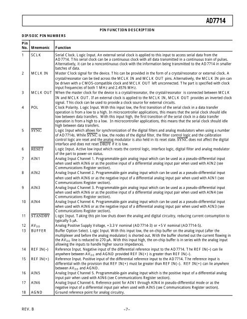
DIP/SOIC PIN NUMBERS<br />
PIN FUNCTION DESCRIPTION<br />
Pin<br />
No. Mnemonic Function<br />
1 SCLK Serial Clock. Logic Input. An external serial clock is applied to this input to access serial data from the<br />
AD7714. This serial clock can be a continuous clock with all data transmitted in a continuous train of pulses.<br />
Alternatively, it can be a noncontinuous clock with the information being transmitted to the AD7714 in smaller<br />
batches of data.<br />
2 MCLK IN Master Clock signal for the device. This can be provided in the form of a crystal/resonator or external clock. A<br />
crystal/resonator can be tied across the MCLK IN and MCLK OUT pins. Alternatively, the MCLK IN pin can<br />
be driven with a <strong>CMOS</strong>-compatible clock and MCLK OUT left unconnected. The part is specified with clock<br />
input frequencies of both 1 MHz and 2.4576 MHz.<br />
3 MCLK OUT When the master clock for the device is a crystal/resonator, the crystal/resonator is connected between MCLK<br />
IN and MCLK OUT. If an external clock is applied to the MCLK IN, MCLK OUT provides an inverted clock<br />
signal. This clock can be used to provide a clock source for external circuits.<br />
4 POL Clock Polarity. Logic Input. With this input low, the first transition of the serial clock in a data transfer<br />
operation is from a low to a high. In microcontroller applications, this means that the serial clock should idle<br />
low between data transfers. With this input high, the first transition of the serial clock in a data transfer<br />
operation is from a high to a low. In microcontroller applications, this means that the serial clock should idle<br />
high between data transfers.<br />
5 SYNC Logic Input which allows for synchronization of the digital filters and analog modulators when using a number<br />
of AD7714s. While SYNC is low, the nodes of the digital filter, the filter control logic and the calibration<br />
control logic are reset and the analog modulator is also held in its reset state. SYNC does not affect the digital<br />
interface and does not reset DRDY if it is low.<br />
6 RESET Logic Input. Active low input which resets the control logic, interface logic, digital filter and analog modulator<br />
of the part to power-on status.<br />
7 AIN1 Analog Input Channel 1. Programmable-gain analog input which can be used as a pseudo-differential input<br />
when used with AIN6 or as the positive input of a differential analog input pair when used with AIN2 (see<br />
Communications Register section).<br />
8 AIN2 Analog Input Channel 2. Programmable-gain analog input which can be used as a pseudo-differential input<br />
when used with AIN6 or as the negative input of a differential analog input pair when used with AIN1 (see<br />
Communications Register section).<br />
9 AIN3 Analog Input Channel 3. Programmable-gain analog input which can be used as a pseudo-differential input<br />
when used with AIN6 or as the positive input of a differential analog input pair when used with AIN4 (see<br />
Communications Register section).<br />
10 AIN4 Analog Input Channel 4. Programmable-gain analog input which can be used as a pseudo-differential input<br />
when used with AIN6 or as the negative input of a differential analog input pair when used with AIN3 (see<br />
Communications Register section).<br />
11 STANDBY Logic Input. Taking this pin low shuts down the analog and digital circuitry, reducing current consumption to<br />
typically 5 µA.<br />
12 AV DD Analog Positive Supply Voltage, +3.3 V nominal (AD7714-3) or +5 V nominal (AD7714-5).<br />
13 BUFFER Buffer Option Select. Logic Input. With this input low, the on-chip buffer on the analog input (after the<br />
multiplexer and before the analog modulator) is shorted out. With the buffer shorted out the current flowing in<br />
the AV DD line is reduced to 270 µA. With this input high, the on-chip buffer is in series with the analog input<br />
allowing the inputs to handle higher source impedances.<br />
14 REF IN(–) Reference Input. Negative input of the differential reference input to the AD7714. The REF IN(–) can lie<br />
anywhere between AV DD and AGND provided REF IN(+) is greater than REF IN(–).<br />
15 REF IN(+) Reference Input. Positive input of the differential reference input to the AD7714. The reference input is<br />
differential with the provision that REF IN(+) must be greater than REF IN(–). REF IN(+) can lie anywhere<br />
between AV DD and AGND.<br />
16 AIN5 Analog Input Channel 5. Programmable-gain analog input which is the positive input of a differential analog<br />
input pair when used with AIN6 (see Communications Register section).<br />
17 AIN6 Analog Input Channel 6. Reference point for AIN1 through AIN4 in pseudo-differential mode or as the<br />
negative input of a differential input pair when used with AIN5 (see Communications Register section).<br />
18 AGND Ground reference point for analog circuitry.<br />
2<br />
REV. B –7–


