

DAC7631 - dreamm
DAC7631 - dreamm
DAC7631 - dreamm

You also want an ePaper? Increase the reach of your titles
YUMPU automatically turns print PDFs into web optimized ePapers that Google loves.
The current into the V REF H input and out of V REF L depends<br />
on the DAC output voltage, and can vary from a few<br />
microamps to approximately 0.3mA in dual supply or 0.15mA<br />
in single-supply operation. The reference input appears as a<br />
varying load to the reference. If the reference can sink or<br />
source the required current, a reference buffer is not required.<br />
The <strong>DAC7631</strong> features a reference drive and sense<br />
connection such that the internal errors caused by the changing<br />
reference current and the circuit impedances can be<br />
minimized. Figures 5 through 13 show different reference<br />
configurations, and the effect on the linearity and differential<br />
linearity.<br />
DIGITAL INTERFACE<br />
Table I shows the basic control logic for the <strong>DAC7631</strong>. The<br />
interface consists of a serial clock input (CLK), serial data<br />
input (SDI), DAC input register load control signal (LOAD),<br />
and DAC load control signal (LDAC). In addition, a chip<br />
select input (CS) is provided to simplify device selection in<br />
systems with multiple devices. An asynchronous reset input<br />
(RST), triggered by a rising edge, is provided to force startup<br />
conditions, periodic resets, or emergency resets to a<br />
known state. The action of RST can be selected using the<br />
reset select (RSTSEL) pin.<br />
SERIAL DATA INPUT<br />
B15 B14 B13 B12 B11 B10 B9 B8 B7 B6 B5 B4 B3 B2 B1 B0<br />
D15 D14 D13 D12 D11 D10 D9 D8 D7 D6 D5 D4 D3 D2 D1 D0<br />
INPUT<br />
DAC<br />
CS RST RSTSEL LDAC LOAD REGISTER REGISTER MODE<br />
L H X X L Write Hold Write Input<br />
H H X ↑ H Hold Write Update<br />
H H X H H Hold Hold Hold<br />
X ↑ L X X Reset to Zero Reset to Zero Reset to Zero<br />
X ↑ H X X Reset to Midscale Reset to Midscale Reset to Midscale<br />
TABLE I. <strong>DAC7631</strong> Logic Truth Table.<br />
+5V<br />
+V<br />
1<br />
V REF H<br />
V CC<br />
20<br />
+<br />
0.1µF 1µF<br />
+2.5V<br />
2<br />
3<br />
V REF H Sense<br />
V REF L<br />
AGND<br />
V SS<br />
19<br />
18<br />
R W1<br />
Serial Data Out<br />
4<br />
5<br />
6<br />
7<br />
V REF L Sense V OUT Sense<br />
DGND<br />
<strong>DAC7631</strong><br />
V DD<br />
SDO<br />
V OUT<br />
NC<br />
RSTSEL<br />
17<br />
16<br />
15<br />
14<br />
R W2<br />
V OUT<br />
Serial Data In<br />
Clock<br />
Chip Select<br />
8<br />
9<br />
10<br />
SDI<br />
CLK<br />
CS<br />
RST<br />
LOAD<br />
LDAC<br />
13<br />
12<br />
11<br />
Reset DAC Registers<br />
Load<br />
Load DAC Registers<br />
FIGURE 4. Analog Output Closed-loop Configuration. R W1 and R W2 represent wiring resistance.<br />
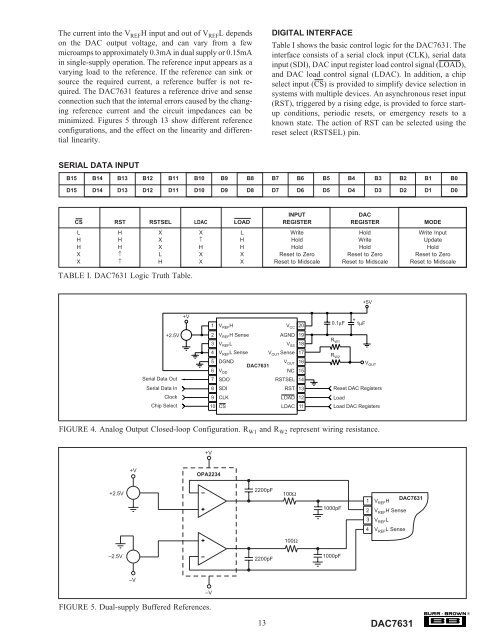
+V<br />
+V<br />
OPA2234<br />
+2.5V<br />
2200pF<br />
100Ω<br />
1000pF<br />
1<br />
2<br />
<strong>DAC7631</strong><br />
V REF H<br />
V REF H Sense<br />
3<br />
V REF L<br />
4<br />
V REF L Sense<br />
100Ω<br />
–2.5V<br />
2200pF<br />
1000pF<br />
–V<br />
–V<br />
FIGURE 5. Dual-supply Buffered References.<br />
13<br />
<strong>DAC7631</strong><br />
®


