DAEWOO CP185 CHASSIS SM.pdf
DAEWOO CP185 CHASSIS SM.pdf DAEWOO CP185 CHASSIS SM.pdf
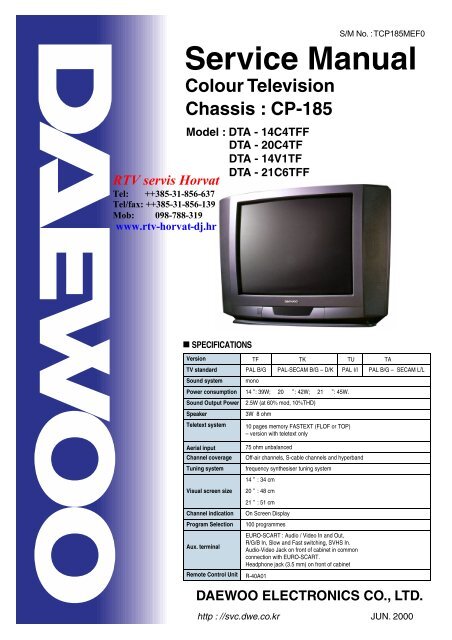
Service Manual Colour Television Chassis : CP-185 Model : DTA - 14C4TFF DTA - 20C4TF DTA - 14V1TF DTA - 21C6TFF RTV servis Horvat Tel: ++385-31-856-637 Tel/fax: ++385-31-856-139 Mob: 098-788-319 www.rtv-horvat-dj.hr S/M No. : TCP185MEF0 SPECIFICATIONS Version TF TK TU TA TV standard PAL B/G PAL-SECAM B/G – D/K PAL I/I PAL B/G – SECAM L/L ’ Sound system mono Power consumption 14 ”: 39W; 20 ”: 42W; 21 ”: 45W. Sound Output Power Speaker Teletext system Aerial input Channel coverage Tuning system Visual screen size Channel indication Program Selection Aux. terminal Remote Control Unit 2.5W (at 60% mod, 10%THD) 3W 8 ohm 10 pages memory FASTEXT (FLOF or TOP) – version with teletext only 75 ohm unbalanced Off-air channels, S-cable channels and hyperband frequency synthesiser tuning system 14 ” : 34 cm 20 ” : 48 cm 21 ” : 51 cm On Screen Display 100 programmes EURO-SCART : Audio / Video In and Out, R/G/B In, Slow and Fast switching, SVHS In. Audio-Video Jack on front of cabinet in common connection with EURO-SCART. Headphone jack (3.5 mm) on front of cabinet R-40A01 DAEWOO ELECTRONICS CO., LTD. http : //svc.dwe.co.kr JUN. 2000
- Page 2 and 3: TABLE OF CONTENTS SAFETY INSTRUCTIO
- Page 4 and 5: SPECIFICATIONS Pin EURO-SCART : 3
- Page 6 and 7: SPECIFICATIONS CH EUROP E CCIR FRAN
- Page 8 and 9: SPECIFICATIONS Special case : Franc
- Page 10 and 11: ALIGNMENT INSTRUCTIONS Microcontrol
- Page 12 and 13: RTV servis Horvat Tel: ++385-31-856
- Page 14 and 15: SERVICE PARTS LIST Caution R is a r
- Page 16 and 17: SERVICE PARTS LIST LOC. PART CODE P
- Page 18 and 19: SERVICE PARTS LIST LOC. PART CODE P
- Page 20 and 21: APPENDIX ALIGNMENT INSTRUCTIONS FUN
- Page 22 and 23: APPENDIX ALIGNMENT INSTRUCTIONS RGB
- Page 24 and 25: APPENDIX ALIGNMENT INSTRUCTIONS Fas
- Page 26 and 27: APPENDIX ALIGNMENT INSTRUCTIONS 8.
- Page 28 and 29: APPENDIX ALIGNMENT INSTRUCTIONS 1 C
- Page 30 and 31: APPENDIX ALIGNMENT INSTRUCTIONS 9-1
- Page 32 and 33: APPENDIX ALIGNMENT INSTRUCTIONS In
- Page 34 and 35: APPENDIX ALIGNMENT INSTRUCTIONS I81
- Page 36 and 37: APPENDIX IC DESCRIPTION Data Captur
- Page 38 and 39: APPENDIX IC DESCRIPTION 19
- Page 40 and 41: APPENDIX IC DESCRIPTION IFIN1 23 IF
- Page 42 and 43: APPENDIX IC DESCRIPTION 2. TDA9830
- Page 44 and 45: APPENDIX IC DESCRIPTION Pinning Sym
- Page 46 and 47: APPENDIX IC DESCRIPTION 5. TDA6107Q
- Page 48 and 49: APPENDIX IC DESCRIPTION 7-3. Block
Service Manual<br />
Colour Television<br />
Chassis : CP-185<br />
Model : DTA - 14C4TFF<br />
DTA - 20C4TF<br />
DTA - 14V1TF<br />
DTA - 21C6TFF<br />
RTV servis Horvat<br />
Tel: ++385-31-856-637<br />
Tel/fax: ++385-31-856-139<br />
Mob: 098-788-319<br />
www.rtv-horvat-dj.hr<br />
S/M No. : T<strong>CP185</strong>MEF0<br />
SPECIFICATIONS<br />
Version TF TK TU TA<br />
TV standard PAL B/G PAL-SECAM B/G – D/K PAL I/I PAL B/G – SECAM L/L ’<br />
Sound system<br />
mono<br />
Power consumption 14 ”: 39W; 20 ”: 42W; 21 ”: 45W.<br />
Sound Output Power<br />
Speaker<br />
Teletext system<br />
Aerial input<br />
Channel coverage<br />
Tuning system<br />
Visual screen size<br />
Channel indication<br />
Program Selection<br />
Aux. terminal<br />
Remote Control Unit<br />
2.5W (at 60% mod, 10%THD)<br />
3W 8 ohm<br />
10 pages memory FASTEXT (FLOF or TOP)<br />
– version with teletext only<br />
75 ohm unbalanced<br />
Off-air channels, S-cable channels and hyperband<br />
frequency synthesiser tuning system<br />
14 ” : 34 cm<br />
20 ” : 48 cm<br />
21 ” : 51 cm<br />
On Screen Display<br />
100 programmes<br />
EURO-SCART : Audio / Video In and Out,<br />
R/G/B In, Slow and Fast switching, SVHS In.<br />
Audio-Video Jack on front of cabinet in common<br />
connection with EURO-SCART.<br />
Headphone jack (3.5 mm) on front of cabinet<br />
R-40A01<br />
<strong>DAEWOO</strong> ELECTRONICS CO., LTD.<br />
http : //svc.dwe.co.kr JUN. 2000
TABLE OF CONTENTS<br />
SAFETY INSTRUCTION .................................................................................................................. 2<br />
SPECIFICATIONS ............................................................................................................................ 3<br />
1. 21 Pin EURO-SCART ................................................................................................................... 3<br />
2. Channel table ............................................................................................................................... 4<br />
3. ATTS sorting method .................................................................................................................... 6<br />
CIRCUIT BLOCK DIAGRAM ........................................................................................................... 8<br />
ALIGNMENT INSTRUCTION ........................................................................................................... 9<br />
1. Service mode ................................................................................................................................ 9<br />
2. Microcontroller configuration ........................................................................................................ 9<br />
3. TV set Alignment .......................................................................................................................... 9<br />
SCHEMATIC DIAGRAM .................................................................................................................. 11<br />
EXPLODED VIEW ............................................................................................................................ 11<br />
PRINTED CIRCUIT BOARD ............................................................................................................ 12<br />
SERVICE PARTS LIST .................................................................................................................... 13<br />
1. The Different Parts List ................................................................................................................. 18<br />
APPENDIX (" Appendix is provided only by internet [http://svc.dwe.co.kr] ")<br />
FUNCTIONAL DESCRIPTION ......................................................................................................... 1<br />
IC DESCRIPTION ............................................................................................................................. 16<br />
1
SAFETY INSTRUCTION<br />
WARNING : Only competent service personnel may carry out work involving the testing or repair of this equipment<br />
X-RAY RADIATION PRECAUTION<br />
1. Excessive high voltage can produce potentially hazardous X-RAY RADIATION. To avoid such hazards, the high<br />
voltage must not exceed the specified limit. The nominal value of the high voltage of this receiver is 22-23 kV (14”) or<br />
24-26 kV (20” - 21”) at max beam current. The high voltage must not, under any circumstances, exceed 27.5 kV (14”,<br />
20”), 29KV (21”). Each time a receiver requires servicing, the high voltage should be checked. It is important to use an<br />
accurate and reliable high voltage meter.<br />
2. The only source of X-RAY Radiation in this TV receiver is the picture tube. For continued X-RAY RADIATION<br />
protection, the replacement tube must be exactly the same type tube as specified in the parts list.<br />
SAFETY PRECAUTION<br />
1. Potentials of high voltage are present when this receiver is operating. Operation of the receiver outside the cabinet or<br />
with the back cover removed involves a shock hazard from the receiver.<br />
1)Servicing should not be attempted by anyone who is not thoroughly familiar with the precautions necessary when<br />
working on high voltage equipment.<br />
2)Discharge the high potential of the picture tube before handling the tube. The picture tube is highly evacuated and if<br />
broken, glass fragments will be violently expelled.<br />
2. If any Fuse in this TV receiver is blown, replace it with the FUSE specified in the Replacement Parts List.<br />
3. When replacing a high wattage resistor (oxide metal film resistor) in circuit board, keep the resistor body 10 mm away<br />
from the circuit board.<br />
4. Keep wires away from high voltage or high temperature components.<br />
5. This receiver must operate under AC 230 volts, 5O Hz. NEVER connect to a DC supply of any other voltage or<br />
frequency.<br />
PRODUCT SAFETY NOTICE<br />
Many electrical and mechanical parts in this equipment have special safety-related characteristics. These characteristics are<br />
often passed unnoticed by a visual inspection and the X-RAY RADIATION protection afforded by them cannot necessarily be<br />
obtained by using replacement components rated for higher voltage, wattage, etc. Replacement parts which have these special<br />
safety characteristics are identified in this manual and its supplements, electrical components having such features are<br />
identified by designated symbol on the parts list. Before replacing any of these components, read the parts list in this manual<br />
carefully. The use of substitutes replacement parts which do not have the same safety characteristics as specified in the parts<br />
list may create X-RAY Radiation.<br />
2
SPECIFICATIONS<br />
Pin EURO-SCART :<br />
3
SPECIFICATIONS<br />
Channel table<br />
FREQUENCY TABLE <strong>CP185</strong><br />
CH<br />
EUROP<br />
E CCIR<br />
FRANCE<br />
GB(IRE-<br />
LAND)<br />
EAST<br />
OIRT<br />
C01 46.25 - 45.75 49.75<br />
C02 48.25 55.75 (L') 53.75 59.25<br />
C03 55.25 60.5 (L') 61.75 77.25<br />
C04 62.25 63.75 (L') 175.25 85.25<br />
C05 175.25 176.00 183.25 93.25<br />
C06 182.25 184.00 191.25 175.25<br />
C07 189.25 192.00 199.25 183.25<br />
C08 196.25 200.00 207.25 191.25<br />
C09 203.25 208.00 215.25 199.25<br />
C10 210.25 216.00 223.25 207.25<br />
C11 217.25 189.25 (LUX) 231.25 215.25<br />
C12 224.25 69.25 (L') 239.25 223.25<br />
C13 53.75 76.25 (L') 247.25 -<br />
C14 - 83.25 (L') 49.75 -<br />
C15 82.25 90.25 57.75 -<br />
C16 - 97.25 65.75 -<br />
C17 183.75 - 77.75 -<br />
C18 192.25 - 85.75 -<br />
C19 201.25 - - -<br />
C20 - - - -<br />
C21 471.25 471.25 471.25 471.25<br />
C22 479.25 479.25 479.25 479.25<br />
C23 487.25 487.25 487.25 487.25<br />
C24 495.25 495.25 495.25 495.25<br />
C25 503.25 503.25 503.25 503.25<br />
C26 511.25 511.25 511.25 511.25<br />
C27 519.25 519.25 519.25 519.25<br />
C28 527.25 527.25 527.25 527.25<br />
C29 535.25 535.25 535.25 535.25<br />
C30 543.25 543.25 543.25 543.25<br />
C31 551.25 551.25 551.25 551.25<br />
C32 559.25 559.25 559.25 559.25<br />
C33 567.25 567.25 567.25 567.25<br />
C34 575.25 575.25 575.25 575.25<br />
C35 583.25 583.25 583.25 583.25<br />
C36 591.25 591.25 591.25 591.25<br />
C37 599.25 599.25 599.25 599.25<br />
C38 607.25 607.25 607.25 607.25<br />
C39 615.25 615.25 615.25 615.25<br />
CH<br />
EUROP<br />
E CCIR<br />
FRANCE<br />
GB(IRE-<br />
LAND)<br />
EAST<br />
OIRT<br />
C40 623.25 623.25 623.25 623.25<br />
C41 631.25 631.25 631.25 631.25<br />
C42 639.25 639.25 639.25 639.25<br />
C43 647.25 647.25 647.25 647.25<br />
C44 655.25 655.25 655.25 655.25<br />
C45 663.25 663.25 663.25 663.25<br />
C46 671.25 671.25 671.25 671.25<br />
C47 679.25 679.25 679.25 679.25<br />
C48 687.25 687.25 687.25 687.25<br />
C49 695.25 695.25 695.25 695.25<br />
C50 703.25 703.25 703.25 703.25<br />
C51 711.25 711.25 711.25 711.25<br />
C52 719.25 719.25 719.25 719.25<br />
C53 727.25 727.25 727.25 727.25<br />
C54 735.25 735.25 735.25 735.25<br />
C55 743.25 743.25 743.25 743.25<br />
C56 751.25 751.25 751.25 751.25<br />
C57 759.25 759.25 759.25 759.25<br />
C58 767.25 767.25 767.25 767.25<br />
C59 775.25 775.25 775.25 775.25<br />
C60 783.25 783.25 783.25 783.25<br />
C61 791.25 791.25 791.25 791.25<br />
C62 799.25 799.25 799.25 799.25<br />
C63 807.25 807.25 807.25 807.25<br />
C64 815.25 815.25 815.25 815.25<br />
C65 823.25 823.25 823.25 823.25<br />
C66 831.25 831.25 831.25 831.25<br />
C67 839.25 839.25 839.25 839.25<br />
C68 847.25 847.25 847.25 847.25<br />
C69 855.25 855.25 855.25 855.25<br />
C70 863.25 863.25 863.25 863.25<br />
C71 69.25 - - -<br />
C72 76.25 - - -<br />
C73 83.25 - - -<br />
C74 90.25 - - -<br />
C75 97.25 - - -<br />
C76 59.25 - - -<br />
C77 93.25 - - -<br />
S01 105.25 104.75 103.25 105.25<br />
4
SPECIFICATIONS<br />
CH<br />
EUROP<br />
E CCIR<br />
FRANCE<br />
GB(IRE-<br />
LAND)<br />
EAST<br />
OIRT<br />
S02 112.25 116.75 111.25 112.25<br />
S03 119.25 128.75 119.25 119.25<br />
S04 126.25 140.75 127.25 126.25<br />
S05 133.25 152.75 135.25 133.25<br />
S06 140.25 164.75 143.25 140.25<br />
S07 147.25 176.75 151.25 147.25<br />
S08 154.25 188.75 159.25 154.25<br />
S09 161.25 200.75 167.25 161.25<br />
S10 168.25 212.75 - 168.25<br />
S11 231.25 224.75 - 231.25<br />
S12 238.25 236.75 - 238.25<br />
S13 245.25 248.75 255.25 245.25<br />
S14 252.25 260.75 263.25 252.25<br />
S15 259.25 272.75 271.25 259.25<br />
S16 266.25 284.75 279.25 266.25<br />
S17 273.25 296.75 287.25 273.25<br />
S18 280.25 136.00 295.25 280.25<br />
S19 287.25 160.00 303.25 287.25<br />
S20 294.25 - - 294.25<br />
S21 303.25 303.25 - 303.25<br />
CH<br />
EUROP<br />
GB(IRE- EAST<br />
FRANCE<br />
E CCIR<br />
LAND) OIRT<br />
S22 311.25 311.25 311.25 311.25<br />
S23 319.25 319.25 319.25 319.25<br />
S24 327.25 327.25 327.25 327.25<br />
S25 335.25 335.25 335.25 335.25<br />
S26 343.25 343.25 343.25 343.25<br />
S27 351.25 351.25 351.25 351.25<br />
S28 359.25 359.25 359.25 359.25<br />
S29 367.25 367.25 367.25 367.25<br />
S30 375.25 375.25 375.25 375.25<br />
S31 383.25 383.25 383.25 383.25<br />
S32 391.25 391.25 391.25 391.25<br />
S33 399.25 399.25 399.25 399.25<br />
S34 407.25 407.25 407.25 407.25<br />
S35 415.25 415.25 415.25 415.25<br />
S36 423.25 423.25 423.25 423.25<br />
S37 431.25 431.25 431.25 431.25<br />
S38 439.25 439.25 439.25 439.25<br />
S39 447.25 447.25 447.25 447.25<br />
S40 455.25 455.25 455.25 455.25<br />
S41 463.25 463.25 463.25 463.25<br />
5
SPECIFICATIONS<br />
ATSS sorting method<br />
The TV set sweeps all the TV bands from beginning of VHF to the end of UHF. The TV controlling software for each program<br />
checks if a VPS CNI code is transmitted. If no VPS CNI code is found, the system checks if a CNI code is transmitted in the teletext<br />
lines ( Packet 8/30 format 1 ). If such a code ( VPS or teletext ) is found and if this code is in the ATSS list, the program is<br />
automatically named.<br />
The programs found are then sorted into 4 groups :<br />
Group I : Contains all the programs from the selected country and named by the TV controlling software. Within this group the<br />
sorting order is fixed by the ATSS list.<br />
Group II : Contains all the programs with a strong signal strength which are not listed in group I.<br />
Group III : Contains all the programs with a weak signal strength which are not listed in group I.<br />
Group IV : If two or more programs with the same code are found, only the strongest (or if they have the same level the one<br />
with the lowest frequency) is listed in group I, II or III. The others are listed in group IV.<br />
Note : If two programs with the same name but a different code are found these two programs are listed in group I, II or III (e.g.<br />
Regional program SW3 in Germany).<br />
The sorting order within group II, III, and IV is based on the channel frequency. The program with the lowest frequency is allocated<br />
the first rank in its group, and so forth until the last program of the group which has the highest frequency.<br />
Program number Group Skip<br />
1<br />
2 Group I<br />
...<br />
n<br />
n+1<br />
... Group II<br />
m<br />
m+1<br />
... Group III<br />
p<br />
p+1<br />
... Group IV<br />
q<br />
q+1<br />
... not used 4<br />
99<br />
0<br />
Program number Group Skip<br />
1<br />
... Group II<br />
m<br />
m+1<br />
... Group III<br />
p<br />
p+1<br />
... Group IV<br />
q<br />
q+1<br />
... not used 4<br />
99<br />
0<br />
Special case : Country selection = Others<br />
Note<br />
For TV versions without teletext, and if the controlling software is unable to catch the station name,<br />
Group I will remain empty.<br />
6
SPECIFICATIONS<br />
Special case : France<br />
If France is selected the TV controlling software firstly sweeps all the TV bands with France system selected (positive video<br />
modulation) and secondly with Europe system selected (negative video modulation).<br />
Special case : Switzerland<br />
If Switzerland is selected the TV controlling software firstly sweeps all the TV bands with Europe system selected (negative<br />
video modulation) and secondly with France system selected (positive video modulation).<br />
Special case : GB<br />
Note for satellite receiver users : Before starting ATSS turn On your satellite receiver and tune “ SKY NEWS “.<br />
If GB is selected the TV controlling software seeks for programs only in UHF ( C21 to C70 ). The sorting order is :<br />
1 - BBC1<br />
2 - BBC2<br />
3 - ITV<br />
4 - CH4<br />
5 - CH5<br />
6 - NEWS<br />
If two or more “ identical “programs ( same name but different code e.g. BBC1 and BBC1 Scotland ) are found the following programs<br />
in the list will be shifted up. (1 - BBC1, 2 - BBC1, 3 - BBC2, 4 - ITV, 5 - CH4, 6 - CH5, 7 - NEWS, ..)<br />
If one of the program above is not found, the associated program number remains empty ( freq.=467.25 MHz - Skip selected -<br />
no name – system = GB).<br />
example A : 1 - BBC1, 2 - BBC2, 3 - ITV, 4 - -----, 5 - CH5, 6 - NEWS, ...<br />
example B ( if 2 BBC1 found ) : 1 - BBC1, 2 - BBC1, 3 - BBC2, 4 - ITV, 5 - -----, 6 - CH5, 7 - NEWS, ...<br />
Version TF TK TU TA<br />
Germany, Belgium,<br />
Spain, Italy,<br />
Austria, Denmark,<br />
Finland,<br />
Germany, Belgium,<br />
Spain, Italy,<br />
Austria, Denmark,<br />
Finland,<br />
GB, Ireland, Others France,<br />
Switzerland,<br />
Germany, Belgium,<br />
Spain, Italy,<br />
ATSS countries Netherlands, Norway,<br />
Sweden,<br />
Others<br />
Netherlands,<br />
Norway, Sweden,<br />
Poland, Hungary,<br />
Czech Rep, Others<br />
Austria, Denmark,<br />
Finland,<br />
Netherlands,<br />
Norway, Sweden,<br />
Others<br />
7
CIRCUIT BLOCK DIAGRAM<br />
8<br />
Base bond signal<br />
#28<br />
#29<br />
Sound processor<br />
I601<br />
Video in<br />
#49<br />
#50<br />
#52<br />
#53<br />
#36<br />
#37 #58<br />
Switching<br />
SCART 1<br />
SIF (5.5MHz for system B/G)<br />
circuit<br />
SCART 2<br />
Audio out<br />
SCART 1<br />
Audio in<br />
SCART 1<br />
RGB out<br />
ext RGB in<br />
chroma in<br />
Trap 5.5MHz<br />
switch control<br />
from #8-I501<br />
and #8 SCART 1<br />
I602<br />
Audio<br />
Amplifier<br />
To speakers /<br />
head phones<br />
IIC BUS<br />
Audio in<br />
SCART 2<br />
To CRT board<br />
#2 #3<br />
#51<br />
#52<br />
#53<br />
#46<br />
#47<br />
#48<br />
IF<br />
#43<br />
#40<br />
I501<br />
Micro controller<br />
video In<br />
video<br />
out<br />
Video processor<br />
#23<br />
#24<br />
Video IF<br />
SF1<br />
QSS<br />
out<br />
#38 #35 #42<br />
#28<br />
#29<br />
ext. video in<br />
Audio IF<br />
SF2<br />
IF = 38.9 MHz (All standard except L')<br />
= 33.9 MHz (L')<br />
#4 - I501
ALIGNMENT INSTRUCTIONS<br />
Microcontroller configuration : Service mode<br />
To switch the TV set into service mode please see instruction below.<br />
1 - Select pr. number 91<br />
2 - Adjust sharpness to minimum and exit all menu.<br />
3 - Quickly press the key sequence : RED - GREEN - menu<br />
To exit SERVICE menu press menu key or Std By key.<br />
In Service Mode press “OK”to stop the microcontroller i.e. the I2C bus is free and the set can be controlled by external equipment.<br />
Press “OK” again to allow the microcontroller to control the set again<br />
Microcontroller configuration :<br />
Tuner Option<br />
Option Tuner maker<br />
DW<br />
<strong>DAEWOO</strong> / SAMSUNG<br />
PH1 PHILIPS ( Video processor AGC )<br />
PH2 PHILIPS (tuner internal AGC )<br />
System Option<br />
Option<br />
TF<br />
TK<br />
TU<br />
TA<br />
System<br />
PAL – B/G<br />
PAL – SECAM B/G-D/K<br />
PAL I/I<br />
PAL – SECAM B/G-L/L’<br />
TV set Alignment<br />
1 - G2 alignment<br />
- Set TV in NORMAL I mode<br />
- TV in AV mode without video signal ? Black screen.<br />
- TV preset with WP Red, WP Green and WP Blue equal to 32.<br />
- TV preset with Black R, Black G equal to 8.<br />
- Adjust screen volume ( on FBT ) such that the highest cathode cut-off voltage measured on CRT board, is Vcut-off ± 5V.<br />
Screen size<br />
Vcut-off<br />
14” 115 V<br />
20” & 21” 125 V<br />
2 - White balance<br />
- Select a dark picture and adjust Black G and Black R to the desired colour temperature.<br />
- Select a bright picture and adjust WP Red, WP Green, WP Blue to the desired colour temperature.<br />
9
ALIGNMENT INSTRUCTIONS<br />
3 - Focus<br />
- Adjust the Focus volume ( on FBT ) to have the best resolution on screen.<br />
4 - Vertical geometry<br />
- Adjust the Vertical Amplitude, Shift, S-Correction and Slope<br />
to compensate for vertical distortion<br />
5 - Horizontal picture centering<br />
- Adjust H Shift to have the picture in the center of the screen.<br />
7 - AGC<br />
- Adjust the antenna signal level to 70 dBµV± 2 for Daewoo tuner (62 dBµV± 2 for Philips tuner).<br />
- Set RF AGC to 0.<br />
- Increase RF AGC level and stop when the level on pin 6 of I501 goes below 2.5 Vdc<br />
10
RTV servis Horvat<br />
Tel: ++385-31-856-637<br />
Tel/fax: ++385-31-856-139<br />
Mob: 098-788-319<br />
www.rtv-horvat-dj.hr<br />
AUDIO<br />
VIDEO
20 19<br />
18<br />
14-1<br />
14<br />
14-2<br />
14-3<br />
17<br />
EXPLODED VIEW<br />
10-1<br />
16-1<br />
7<br />
10<br />
16<br />
11<br />
8<br />
20<br />
4858193401<br />
PAD<br />
1<br />
EPS 20D5<br />
10<br />
10-1<br />
15<br />
19<br />
18<br />
17<br />
4858211800<br />
4858055200<br />
4855415800<br />
BAG PE<br />
CARTON BOX<br />
SPEC PLATE<br />
1<br />
1<br />
1<br />
LDPE T0.03X1300X1000<br />
DW-3<br />
150 ART P/E FILM(C/TV)<br />
16-1<br />
7172401412<br />
SCREW TAPPTITE<br />
5 TT2 TRS 4X14 MFZN BK<br />
16<br />
4852155601<br />
COVER BACK<br />
1<br />
HIPS BK<br />
15<br />
14-3<br />
4856214902<br />
4856013302<br />
MAIN PCB<br />
SCREW CRT FIXING AS<br />
1<br />
2<br />
30X190 BK<br />
6<br />
9<br />
9-1<br />
11<br />
12<br />
14-2<br />
14-1<br />
14<br />
13<br />
12<br />
11<br />
4856013300<br />
4856215402<br />
4851915401<br />
4854945801<br />
4855541201<br />
SCREW CRT FIXING AS<br />
RUBBER<br />
CRT<br />
BUTTON CTRL<br />
BUTTON<br />
DECO SENSOR<br />
2<br />
4<br />
1<br />
30X80 BK<br />
CR T2.0<br />
1 4945801+5541201<br />
1 HIPS BK<br />
1 PMMA MILKY<br />
10<br />
4857618000<br />
INSU PLATE<br />
1<br />
PVC T1.0<br />
9-1<br />
13<br />
9-1<br />
9<br />
7128301212<br />
SCREW TAPPTIE<br />
SPEAKER<br />
8<br />
2<br />
TT2 WAS 3X12 MFZN BK<br />
9<br />
8<br />
7<br />
4852073601<br />
4855313101<br />
MASK FRONT<br />
DECO COVER<br />
1 HIPS BK<br />
1<br />
PC BK<br />
1<br />
2<br />
3<br />
4<br />
4-1<br />
6<br />
5<br />
4-1<br />
4855617500<br />
4852067101<br />
7128301212<br />
MARK BRAND<br />
PANEL FRONT<br />
SCREW TAPPTIE<br />
1<br />
1<br />
2<br />
CUAU+ABS BK<br />
2326511+4856401+6716000<br />
TT2 WAS 3X12 MFZN BK<br />
4<br />
4852326511<br />
PANEL<br />
1<br />
HIPS BK<br />
5<br />
3<br />
2<br />
1<br />
4856716000<br />
4854856401<br />
4852539601<br />
SPRING<br />
BUTTON POWER<br />
GRILL<br />
1 SWPA PIE 0.5<br />
1<br />
2<br />
ABS BK<br />
EGI T0.5<br />
No<br />
PART CODE<br />
PART NAME<br />
Q'ty<br />
MATERIAL<br />
REMARKS
SERVICE PARTS LIST<br />
Caution<br />
R<br />
is a recommendable part for stock.<br />
is safety component, so it must be used the same component.<br />
LOC. PART CODE PART NAME PART DESCRIPTION<br />
ZZ110 PTACPWA21C6A ACCESSORY AS DTA-21C6TAF<br />
00100 4850Q00910P BATTERY <strong>DAEWOO</strong> AAA<br />
M821 4858213800 BAG POLY L.D.P.E.T0.5X250X40 MILK<br />
ZZ100 R 48B3740A01<br />
TRAN<strong>SM</strong>ITTER<br />
R-40A01<br />
REMOCON<br />
ZZ120 PTBCSHD616 COVER BACK AS DTP-21C6TFP<br />
M211 4852151601 COVER BACK HIPS BK 21V1, V4, C6<br />
M541 4855415800 S/PLATE 150ART P/E FILM (C/TV)<br />
M542 4855800022 LABEL SERIAL ART 90 70X19<br />
ZZ130 PTPKCPA21C6A PACKING AS DTA-21C6TAF<br />
10 6520010200 STAPLE PIN #3417 ALL<br />
20 6520010200 STAPLE PIN #3417 ALL<br />
M811 4858190700 PAD EPS 21C6<br />
M821 4858211801 BAG P.E. PE FILM T0.05X1300X1000<br />
ZZ140 PTCACAA21C6AF CABINET AS DTA-21C6TAF<br />
M191 4854943202 BUTTON CONTROL 21C6<br />
M201A 4856013301<br />
SCREW CRT FIXING<br />
L-140<br />
AS<br />
M201B 4856215402 WASHER RUBBER 20''<br />
M201C 4856013303<br />
SCREW CRT FIXING<br />
L-240<br />
AS<br />
M211A 7172401412 SCREW TAPPING TT2 TRS 4X14 MFZN BK<br />
M211D 7172401412 SCREW TAPPING TT2 TRS 4X14 MFZN BK<br />
M481 4854943203 BUTTON POWER ABS BK 21C6<br />
M551 4855538000 DECO SENSOR 21C6<br />
M561 485562140101 MARK BRAND <strong>DAEWOO</strong> 14/20/21/C4/C6<br />
M681 4856812001 TIE CABLE NYLON66 DA100<br />
P402A 4850706N06 CONN AS 35135-0620+35719+ULW=550<br />
PWC1 4859906210 CORD POWER FTZ (LOMAX NEW TYPE)<br />
SP01A 7178301011 SCREW TAPPING TT2 WAS 3X10 MFZN<br />
V901 R 4859607660C CRT (PHILIPS 21") A51EAL155X17 (CONN AS)<br />
ZZ131 58G0000074 COIL DEGAUSSING 21" DC-2070<br />
ZZ132 48519A5310 CRT GROUND AS 2101S-1015-1P<br />
ZZ200 R PTFMSJD616 MASK FRONT AS DTP-21C6TFP<br />
M201 4852071401 MASK FRONT HIPS BK 21C6<br />
ZZ210 PTSPPWA615 SPEAKER AS DTP-14C4TFD<br />
P601A 4850703S50 CONN AS YH025-03+3509=200<br />
SP01 R 4858314010 SPEAKER SP-5070F01 3W 8 OHM<br />
ZZ290 PTMPMSA21C6AF<br />
PCB MAIN MANUAL<br />
DTA-21C6TAF<br />
AS<br />
10 2193100801 SOLDER BAR SN:PB=63:37 3PI(NO FLUX)<br />
40 2291050314 FLUX SOLVENT IM-1000<br />
20 2193011101 SOLDER WIRE RS 60-1.2 1.6A<br />
30 2291050617P FLUX SOLDER CF-329D<br />
50 2291140501 WAX COVER 60G/PC<br />
60 2291051001 FLUX KILLER KFT-7<br />
C315 CEXF2C470C C ELECTRO 160V RUS 47MF (13X25) TP<br />
C404 CMYT3C822J C MYLAR 1.6KV 8200PF MKP<br />
C408 CMYE2D364J C MYLAR 200V 0.36MF J (PL)<br />
LOC. PART CODE PART NAME PART DESCRIPTION<br />
C415 CEXF2E100V C ELECTRO 250V RSS 10MF (10X20) TP<br />
C603 CEXF1C471V C ELECTRO 16V RSS 470MF (10X12.5)TP<br />
C801 CL1SC3474M C LINE ACROSS 275V 0.47MF<br />
C805 R CEYN2G121P C ELECTRO 400V LHS 120MF<br />
C810 CCXB3D102K C CERA 2KV B 1000 PF K (TAPPING)<br />
C812 R CH1AFE472M C CERA AC 4KV 4700PF M KX DE1610<br />
C813 CEXF2C101V C ELECTRO 160V RSS 100MF (16X25) TP<br />
C814 CEXF2C101V C ELECTRO 160V RSS 100MF (16X25) TP<br />
C820 CCXB3A471K C CERA 1KV B 470PF K (T)<br />
C823 CEXF1E102V C ELECTRO 25V RSS 1000MF (13X20) TP<br />
C824 CCXB3A471K C CERA 1KV B 470PF K (T)<br />
C831 CCXB3A471K C CERA 1KV B 470PF K (T)<br />
C832 CEXF1E102V C ELECTRO 25V RSS 1000MF (13X20) TP<br />
C840 CEXF1C222V C ELECTRO 16V RSS 2200MF(13X25)TP<br />
C841 CEXF1C222V C ELECTRO 16V RSS 2200MF(13X25)TP<br />
C861 CEXF1E102V C ELECTRO 25V RSS 1000MF (13X20) TP<br />
C866 CCXB3A471K C CERA 1KV B 470PF K (T)<br />
C965 CCXB3D102K C CERA 2KV B 1000 PF K (TAPPING)<br />
D403 DBY228---- DIODE BY228<br />
D707 D<strong>SM</strong>L1216W- LED <strong>SM</strong>L1216W<br />
D820 DBYW76---- DIODE BYW76<br />
F801 5FSCB4022R FUSE CERA SEMKO F4AH 4A 250V MF51<br />
G900 4SG0D00103 SPARK GAP S-23 900V-1.5KV<br />
I101 1TDA9830-- IC RF TDA9830<br />
I301 R 1TDA8357J- IC VERTICAL TDA8357J<br />
I301A 4857025405 HEAT SINK A1050P-H24 (CP-185)<br />
I301B 7174301011 SCREW TAPPTITE TT2 RND 3X10 MFZN<br />
I501 R 1TDA9361-- IC MAIN TDA9361PS/N1/3<br />
I601 R 1TDA7267A- IC AMP TDA7267A<br />
I702 1AT24C08PC IC MEMORY AT24C08-10PC<br />
I703 1KRT30---- IC PREAMP KRT30<br />
I801 R 1STRF6653- IC <strong>SM</strong>PS STR-F6653<br />
I801A 4857024618 HEAT SINK I801A (CP-385 AIWA)<br />
I801B 7174300811 SCREW TAPPTITE TT2 RND 3X8 MFZN<br />
I804 1LTV817C-- IC PHOTO COUPLER LTV-817C<br />
I806 1SE110N--- IC SE110N<br />
I810 TX0202DA-- THYRISTOR X0202DA<br />
I820 1KA7805--- IC REGULATOR KA7805<br />
I822 1KA7808--- IC REGULATOR KA7808<br />
I823 1LE33CZ--- IC REGULATOR LE33CZ<br />
I901 1TDA6107Q- IC VIDEO TDA6107Q<br />
I901A 4857031100 HEAT SINK A1050P-H24 T2.0<br />
I901B 7174301011 SCREW TAPPTITE TT2 RND 3X10 MFZN<br />
JPA1 4859200401 SOCKET RGB SR-21A1 (ANGLE TYPE)<br />
JS1 4859109950 JACK PIN BOARD PH-JB-9710A<br />
L401 58H0000016 COIL H-LINEARITY L-102 (102UH)<br />
L802 58C9430599 COIL CHOKE AZ-9004Y(94MH)<br />
LF801 5PLF24A1-- FILTER LINE LF-24A1<br />
M351 4853533600 HOLDER LED P.P BK<br />
13
SERVICE PARTS LIST<br />
LOC. PART CODE PART NAME PART DESCRIPTION<br />
M791 4857913304 RUBBER CUSION FR RUBBER SPONGE<br />
P401 4850705N18 CONN AS BIC-05T-25T+ULW=400<br />
P402 4859240120 CONN WAFER YFW500-06<br />
P501 4850705N14 CONNECTOR BIC-05T-25T+ULW=500<br />
P601 4859231620 CONN WAFER YW025-03<br />
P801 4859287320 CONN WAFER MKS2822 (LOMAX NEW TYPE)<br />
P802 4859242220 CONN WAFER YFW800-02<br />
Q401 R T2SD2499-- TR 2SD2499<br />
R305 RS02Y331JS R M-OXIDE FILM 2W 330 OHM J <strong>SM</strong>ALL<br />
R415 RS02Y102JS R M-OXIDE FILM 2W 1K OHM J <strong>SM</strong>ALL<br />
R450 RS02Y103JS R M-OXIDE FILM 2W 10K OHM J <strong>SM</strong>ALL<br />
R801 DT120B8010 POSISTOR T120-B80-A110<br />
R802 RS02Y753JS R M-OXIDE FILM 2W 75K OHM J <strong>SM</strong>ALL<br />
R803 RS02Y473JS R M-OXIDE FILM 2W 47K OHM J <strong>SM</strong>ALL<br />
R804 RF02Y338K- R FUSIBLE 2W 0.33 OHM K<br />
R808 RS02Y821JS R M-OXIDE FILM 2W 820 OHM J <strong>SM</strong>ALL<br />
R819 RX07C339JF R CEMENT 7W 3.3 OHM J 15MM 4P<br />
R920 RF01Y209JA R FUSIBLE 1W 2 OHM J A CURVE<br />
SCT1 4859303530 SOCKET CRT PCS629-03C<br />
SF1 5PG1984M-- FILTER SAW G1984M<br />
SF2 5PL9653M-- FILTER SAW L9653M<br />
SW801 R 5S40101146 SW POWER PUSH SS-160-7-B<br />
T401 R 50D10A2--- TRANS DRIVE TD-10A2<br />
T402 R 50H0000211 FBT 1142.5109<br />
T801 20745046-- TRANS <strong>SM</strong>PS 2074.5046<br />
U100 R 4859720730 TUNER VARACTOR UV1316/A<br />
X502 5XE12R000E CRYSTAL QUARTZ HC-49/U 12.00000MHZ 30PPM<br />
Z501 5PXPS5R5MB FILTER CERA TPS5.5MB-TF21 TAPING<br />
ZZ200 PTMPJRA21C6AF PCB MAIN RADIAL AS DTA-21C6TAF<br />
C101 CEXF1H100V C ELECTRO 50V RSS 10MF (5X11) TP<br />
C102 CEXF1H470V C ELECTRO 50V RSS 47MF (6.3*11) TP<br />
C106 CEXF1E221V C ELECTRO 25V RSS 220MF (8X11.5) TP<br />
C120 CCXB1H102K C CERA 50V B 1000PF K (TAPPING)<br />
C121 CEXF1H100V C ELECTRO 50V RSS 10MF (5X11) TP<br />
C152 CEXF1H229V C ELECTRO 50V RSS 2.2MF (5X11) TP<br />
C153 CBXF1H104Z C CERA SEMI 50V F 0.1MF Z (TAPPING)<br />
C154 CEXF1H479V C ELECTRO 50V RSS 4.7MF (5*11) TP<br />
C155 CEXF1H479V C ELECTRO 50V RSS 4.7MF (5*11) TP<br />
C156 CEXF1H479V C ELECTRO 50V RSS 4.7MF (5*11) TP<br />
C305 CEXF1E221V C ELECTRO 25V RSS 220MF (8X11.5) TP<br />
C313 CBXF1H104Z C CERA SEMI 50V F 0.1MF Z (TAPPING)<br />
C320 CBXF1H104Z C CERA SEMI 50V F 0.1MF Z (TAPPING)<br />
C390 CMXM2A473J C MYLAR 100V 0.047MF J TP<br />
C401 CEXF1H470V C ELECTRO 50V RSS 47MF (6.3*11) TP<br />
C412 CEXF2C339V C ELECTRO 160V RSS 3.3MF (8X16) TP<br />
C414 CMXM2A104J C MYLAR 100V 0.1MF J TP<br />
C417 CMXL2E104K C MYLAR 250V 0.1MF K MEU TP<br />
C418 CCXB1H102K C CERA 50V B 1000PF K (TAPPING)<br />
C420 CCXB2H222K C CERA 500V B 2200PF K (TAPPING)<br />
LOC. PART CODE PART NAME PART DESCRIPTION<br />
C500 CEXF1H478V C ELECTRO 50V RSS 0.47MF (5X11) TP<br />
C501 CEXF1H100V C ELECTRO 50V RSS 10MF (5X11) TP<br />
C502 CEXF1H100V C ELECTRO 50V RSS 10MF (5X11) TP<br />
C504 CMXM2A332J C MYLAR 100V 3300PF J TP<br />
C509 CEXF1E470V C ELECTRO 25V RSS 47MF (5X11) TP<br />
C511 CMXB1H224J C MYLAR 50V EU 0.22MF J(TP)<br />
C512 CMXB1H224J C MYLAR 50V EU 0.22MF J(TP)<br />
C513 CBXF1H104Z C CERA SEMI 50V F 0.1MF Z (TAPPING)<br />
C514 CEXF1E101V C ELECTRO 25V RSS 100MF (6.3X11) TP<br />
C517 CEXF1H109V C ELECTRO 50V RSS 1MF (5X11) TP<br />
C519 CEXF1H229V C ELECTRO 50V RSS 2.2MF (5X11) TP<br />
C522 CEXF1H479V C ELECTRO 50V RSS 4.7MF (5*11) TP<br />
C524 CMXB1H104J C MYLAR 50V EU 0.1MF J (TP)<br />
C525 CCXB1H102K C CERA 50V B 1000PF K (TAPPING)<br />
C526 CMXB1H104J C MYLAR 50V EU 0.1MF J (TP)<br />
C527 CMXM2A473J C MYLAR 100V 0.047MF J TP<br />
C528 CEXF1E101V C ELECTRO 25V RSS 100MF (6.3X11) TP<br />
C530 CEXF1C101V C ELECTRO 16V RSS 100MF (6.3X11) TP<br />
C532 CEXF1H100V C ELECTRO 50V RSS 10MF (5X11) TP<br />
C533 CCXB1H102K C CERA 50V B 1000PF K (TAPPING)<br />
C537 CBXF1H104Z C CERA SEMI 50V F 0.1MF Z (TAPPING)<br />
C555 CEXF1C470V C ELECTRO 16V RSS 47MF (5X11) TP<br />
C560 CBXF1H104Z C CERA SEMI 50V F 0.1MF Z (TAPPING)<br />
C564 CEXF1E101V C ELECTRO 25V RSS 100MF (6.3X11) TP<br />
C565 CBXF1H104Z C CERA SEMI 50V F 0.1MF Z (TAPPING)<br />
C570 CCXB1H472K C CERA 50V B 4700PF K (TAPPING)<br />
C571 CCXB1H821K C CERA 50V B 820PF K (TAPPING)<br />
C585 CCXB1H222K C CERA 50V B 2200PF K (TAPPING)<br />
C590 CXCH1H270J C CERA 50V CH 27PF J (TAPPING)<br />
C591 CXCH1H270J C CERA 50V CH 27PF J (TAPPING)<br />
C592 CBXF1H104Z C CERA SEMI 50V F 0.1MF Z (TAPPING)<br />
C593 CEXF1E101V C ELECTRO 25V RSS 100MF (6.3X11) TP<br />
C599 CEXF1H229V C ELECTRO 50V RSS 2.2MF (5X11) TP<br />
C600 CEXF1E101V C ELECTRO 25V RSS 100MF (6.3X11) TP<br />
C601 CEXF1H108V C ELECTRO 50V RSS 0.1MF (5X11) TP<br />
C602 CCXF1H103Z C CERA 50V F 0.01MF Z (TAPPING)<br />
C650 CEXF1E470V C ELECTRO 25V RSS 47MF (5X11) TP<br />
C770 CEXF1C101V C ELECTRO 16V RSS 100MF (6.3X11) TP<br />
C803 CCXF3A472Z C CERA 1KV F 4700PF Z (T)<br />
C804 CCXF3A472Z C CERA 1KV F 4700PF Z (T)<br />
C806 CEXF1H330V C ELECTRO 50V RSS 33MF (6.3X11) TP<br />
C807 CCXF1H473Z C CERA 50V F 0.047MF Z (TAPPING)<br />
C808 CEXF1H479V C ELECTRO 50V RSS 4.7MF (5*11) TP<br />
C821 CCXB1H102K C CERA 50V B 1000PF K (TAPPING)<br />
C835 CEXF1H470V C ELECTRO 50V RSS 47MF (6.3*11) TP<br />
C844 CEXF1E101V C ELECTRO 25V RSS 100MF (6.3X11) TP<br />
C863 CEXF1E101V C ELECTRO 25V RSS 100MF (6.3X11) TP<br />
C888 CEXF1C470V C ELECTRO 16V RSS 47MF (5X11) TP<br />
C910 CCXB1H152K C CERA 50V B 1500PF K (TAPPING)<br />
14
SERVICE PARTS LIST<br />
LOC. PART CODE PART NAME PART DESCRIPTION<br />
C968 CMXL2E104K C MYLAR 250V 0.1MF K MEU TP<br />
CA04 CEXD1H229F C ELECTRO 50V RND 2.2MF (5X11) TP<br />
CA05 CCXB1H102K C CERA 50V B 1000PF K (TAPPING)<br />
F801A 4857415001 CLIP FUSE PFC5000-0702<br />
F801B 4857415001 CLIP FUSE PFC5000-0702<br />
Q101 T2SC5343Y- TR 2SC5343Y<br />
Q152 T2SC5343Y- TR 2SC5343Y<br />
Q154 T2SC5343Y- TR 2SC5343Y<br />
Q155 T2SC5343Y- TR 2SC5343Y<br />
Q402 T2SD1207T- TR 2SD1207-T (TAPPING)<br />
Q501 TSTA933Y-- TR STA933-Y<br />
Q502 T2SC5343Y- TR 2SC5343Y<br />
Q503 T2SC5343Y- TR 2SC5343Y<br />
Q510 TSTA933Y-- TR STA933-Y<br />
Q511 TSTA933Y-- TR STA933-Y<br />
Q520 T2SC5343Y- TR 2SC5343Y<br />
Q807 T2SC5343Y- TR 2SC5343Y<br />
Q808 T2SC5343Y- TR 2SC5343Y<br />
Q809 T2SC5343Y- TR 2SC5343Y<br />
Q810 T2SC5343Y- TR 2SC5343Y<br />
Q811 T2SC5343Y- TR 2SC5343Y<br />
SW700 5S50101090 SW TACT SKHV17910A<br />
SW701 5S50101090 SW TACT SKHV17910A<br />
SW702 5S50101090 SW TACT SKHV17910A<br />
SW703 5S50101090 SW TACT SKHV17910A<br />
SW704 5S50101090 SW TACT SKHV17910A<br />
Z603 5PXF1B471M FILTER EMI CFI 06 B 1H 470PF<br />
Z605 5PXF1B471M FILTER EMI CFI 06 B 1H 470PF<br />
Z606 5PXF1B471M FILTER EMI CFI 06 B 1H 470PF<br />
Z630 5PXF1B471M FILTER EMI CFI 06 B 1H 470PF<br />
ZZ200 PTMPJAA21C6AF PCB MAIN AXIAL AS DTA-21C6TAF<br />
10 2TM10006LB TAPE MASKING 3M #232-MAP-C 6.2X2000M<br />
20 2TM14006LB TAPE MASKING 3M #232 6.0X2000M<br />
A001 4859804593 PCB MAIN 246X246 CP-185<br />
C103 CCZB1H102K C CERA 50V B 1000PF K (AXIAL)<br />
C104 CCZB1H102K C CERA 50V B 1000PF K (AXIAL)<br />
C150 CCZF1H103Z C CERA 50V F 0.01MF Z<br />
C350 CCZF1H473Z C CERA 50V F 0.047MF Z AXIAL<br />
C351 CCZF1H473Z C CERA 50V F 0.047MF Z AXIAL<br />
C515 CBZR1C222M C CERA Y5R 16V 2200PF M AXIAL<br />
C516 CCZB1H472K C CERA 50V B 4700PF K (AXIAL)<br />
C518 CBZF1H104Z C CERA SEMI 50V F 0.1MF Z (AXIAL)<br />
C520 CCZB1H102K C CERA 50V B 1000PF K (AXIAL)<br />
C521 CCZB1H102K C CERA 50V B 1000PF K (AXIAL)<br />
C523 CCZF1H103Z C CERA 50V F 0.01MF Z<br />
C529 CBZF1H104Z C CERA SEMI 50V F 0.1MF Z (AXIAL)<br />
C531 CCZF1H473Z C CERA 50V F 0.047MF Z AXIAL<br />
C534 CCZF1H223Z C CERA 50V F 0.022MF Z<br />
C535 CCZF1H223Z C CERA 50V F 0.022MF Z<br />
LOC. PART CODE PART NAME PART DESCRIPTION<br />
C536 CCZF1H223Z C CERA 50V F 0.022MF Z<br />
C577 CCZB1H561K C CERA 50V B 560PF K (AXIAL)<br />
C587 CCZB1H101K C CERA 50V B 100PF K (AXIAL)<br />
C588 CCZB1H101K C CERA 50V B 100PF K (AXIAL)<br />
C589 CCZB1H101K C CERA 50V B 100PF K (AXIAL)<br />
C771 CBZF1H104Z C CERA SEMI 50V F 0.1MF Z (AXIAL)<br />
C809 CCZB1H102K C CERA 50V B 1000PF K (AXIAL)<br />
C830 CBZF1H104Z C CERA SEMI 50V F 0.1MF Z (AXIAL)<br />
C850 CCZB1H821K C CERA 50V B 820PF K (AXIAL)<br />
CA01 CCZB1H101K C CERA 50V B 100PF K (AXIAL)<br />
CA02 CCZB1H101K C CERA 50V B 100PF K (AXIAL)<br />
CA03 CCZB1H101K C CERA 50V B 100PF K (AXIAL)<br />
CA10 CCZB1H102K C CERA 50V B 1000PF K (AXIAL)<br />
D101 DBAT85---- DIODE BAT85 (TAPPING)<br />
D151 D1SS85TA-- DIODE 1SS85TA<br />
D313 DBYW36---- DIODE BYW36 (TAPPING)<br />
D341 DUZ33B---- DIODE ZENER UZ-33B<br />
D350 DTZX12C--- DIODE ZENER TZX12C (TAPPING)<br />
D360 DTZX22C--- DIODE ZENER TZX22C (TAPPING)<br />
D361 DUZ33B---- DIODE ZENER UZ-33B<br />
D405 DBYW36---- DIODE BYW36 (TAPPING)<br />
D407 DBYW36---- DIODE BYW36 (TAPPING)<br />
D408 DBYW36---- DIODE BYW36 (TAPPING)<br />
D450 DBYW36---- DIODE BYW36 (TAPPING)<br />
D510 DUZ3R9B--- DIODE ZENER UZ-3.9B<br />
D511 DUZ3R9B--- DIODE ZENER UZ-3.9B<br />
D520 D1N4148--- DIODE 1N4148 (TAPPING)<br />
D521 D1N4148--- DIODE 1N4148 (TAPPING)<br />
D591 DTZX2V4A-- DIODE ZENER TZX2V4A<br />
D710 DTZX5V1B-- DIODE ZENER TZX5V1B (TAPPING)<br />
D801 DBYT51J--- DIODE BYT51J (TAPPING)<br />
D802 DBYT51J--- DIODE BYT51J (TAPPING)<br />
D803 DBYT51J--- DIODE BYT51J (TAPPING)<br />
D804 DBYT51J--- DIODE BYT51J (TAPPING)<br />
D805 DBYW36---- DIODE BYW36 (TAPPING)<br />
D806 DBYW36---- DIODE BYW36 (TAPPING)<br />
D808 DBYW36---- DIODE BYW36 (TAPPING)<br />
D809 DBYW36---- DIODE BYW36 (TAPPING)<br />
D810 DBYW36---- DIODE BYW36 (TAPPING)<br />
D811 DTZX5V6B-- DIODE ZENER TZX5V6B (TAPPING)<br />
D821 DBYW36---- DIODE BYW36 (TAPPING)<br />
D822 DTZX9V1B-- DIODE ZENER TZX9V1B (TAPPING)<br />
D824 D1N4148--- DIODE 1N4148 (TAPPING)<br />
D825 D1N4148--- DIODE 1N4148 (TAPPING)<br />
D830 DBYW36---- DIODE BYW36 (TAPPING)<br />
D831 DBYW36---- DIODE BYW36 (TAPPING)<br />
D840 D1N4148--- DIODE 1N4148 (TAPPING)<br />
D841 D1N4148--- DIODE 1N4148 (TAPPING)<br />
D860 DBYW36---- DIODE BYW36 (TAPPING)<br />
15
SERVICE PARTS LIST<br />
LOC. PART CODE PART NAME PART DESCRIPTION<br />
D904 DBAV21---- DIODE BAV21 (TAPPING)<br />
D905 DBAV21---- DIODE BAV21 (TAPPING)<br />
D906 DBAV21---- DIODE BAV21 (TAPPING)<br />
DA02 DTZX12C--- DIODE ZENER TZX12C (TAPPING)<br />
DA03 DTZX5V1B-- DIODE ZENER TZX5V1B (TAPPING)<br />
DA04 CBZR1C222M C CERA Y5R 16V 2200PF M AXIAL<br />
DA05 DTZX5V6B-- DIODE ZENER TZX5V6B (TAPPING)<br />
DA06 DTZX5V6B-- DIODE ZENER TZX5V6B (TAPPING)<br />
DA08 DTZX5V6B-- DIODE ZENER TZX5V6B (TAPPING)<br />
DA09 DTZX5V6B-- DIODE ZENER TZX5V6B (TAPPING)<br />
DA10 DTZX5V6B-- DIODE ZENER TZX5V6B (TAPPING)<br />
DA11 DTZX5V6B-- DIODE ZENER TZX5V6B (TAPPING)<br />
DA27 DTZX5V6B-- DIODE ZENER TZX5V6B (TAPPING)<br />
JAMP<br />
85801065GY WIRE COPPER AWG22 1/0.65 TIN COATING<br />
WIRES<br />
L101 5CPZ100K02 COIL PEAKING 10UH 3.5MM K (LAL02TB)<br />
L301 5CPZ109M04 COIL PEAKING 1UH 10.5MM M (LAL04TB)<br />
L350 5CPZ109M04 COIL PEAKING 1UH 10.5MM M (LAL04TB)<br />
L351 85801065GY WIRE COPPER AWG22 1/0.65 TIN COATING<br />
L500 5CPZ120K02 COIL PEAKING 12UH 3.5MM K (LAL02TB)<br />
L501 5CPZ100K02 COIL PEAKING 10UH 3.5MM K (LAL02TB)<br />
L502 5CPZ100K02 COIL PEAKING 10UH 3.5MM K (LAL02TB)<br />
L510 5CPZ100K02 COIL PEAKING 10UH 3.5MM K (LAL02TB)<br />
L511 5CPZ100K02 COIL PEAKING 10UH 3.5MM K (LAL02TB)<br />
L512 5CPZ100K02 COIL PEAKING 10UH 3.5MM K (LAL02TB)<br />
L600 5MC0000100 COIL BEAD MD-5 (HC-3550)<br />
L801 5MC0000100 COIL BEAD MD-5 (HC-3550)<br />
L803 5MC0000100 COIL BEAD MD-5 (HC-3550)<br />
R101 RD-AZ473J- R CARBON FILM 1/6 47K OHM J<br />
R102 RD-AZ472J- R CARBON FILM 1/6 4.7K OHM J<br />
R103 RD-AZ123J- R CARBON FILM 1/6 12K OHM J<br />
R104 RD-AZ104J- R CARBON FILM 1/6 100K OHM J<br />
R105 RD-AZ392J- R CARBON FILM 1/6 3.9K OHM J<br />
R106 RD-AZ101J- R CARBON FILM 1/6 100 OHM J<br />
R107 RD-AZ101J- R CARBON FILM 1/6 100 OHM J<br />
R120 RD-AZ101J- R CARBON FILM 1/6 100 OHM J<br />
R153 RD-AZ222J- R CARBON FILM 1/6 2.2K OHM J<br />
R156 RD-AZ163J- R CARBON FILM 1/6 16K OHM J<br />
R157 RD-AZ562J- R CARBON FILM 1/6 5.6K OHM J<br />
R159 RD-AZ222J- R CARBON FILM 1/6 2.2K OHM J<br />
R160 RD-AZ682J- R CARBON FILM 1/6 6.8K OHM J<br />
R161 RD-AZ102J- R CARBON FILM 1/6 1K OHM J<br />
R162 RD-AZ473J- R CARBON FILM 1/6 47K OHM J<br />
R163 RD-AZ103J- R CARBON FILM 1/6 10K OHM J<br />
R164 RD-AZ101J- R CARBON FILM 1/6 100 OHM J<br />
R170 RD-AZ133J- R CARBON FILM 1/6 13K OHM J<br />
R302 RD-2Z159J- R CARBON FILM 1/2 1.5 OHM J<br />
R310 RD-AZ102J- R CARBON FILM 1/6 1K OHM J<br />
R311 RD-AZ102J- R CARBON FILM 1/6 1K OHM J<br />
LOC. PART CODE PART NAME PART DESCRIPTION<br />
R340 RD-4Z473J- R CARBON FILM 1/4 47K OHM J<br />
R341 RD-2Z332J- R CARBON FILM 1/2 3.3K OHM J<br />
R350 RN-4Z2001F R METAL FILM 1/4 2.0K OHM F<br />
R351 RN-4Z2001F R METAL FILM 1/4 2.0K OHM F<br />
R355 RD-AZ272J- R CARBON FILM 1/6 2.7K OHM J<br />
R356 RD-4Z562J- R CARBON FILM 1/4 5.6K OHM J<br />
R360 RD-4Z564J- R CARBON FILM 1/4 560K OHM J<br />
R390 RD-4Z159J- R CARBON FILM 1/4 1.5 OHM J<br />
R401 RD-4Z272J- R CARBON FILM 1/4 2.7K OHM J<br />
R404 RD-4Z399J- R CARBON FILM 1/4 3.9 OHM J<br />
R420 RD-AZ223J- R CARBON FILM 1/6 22K OHM J<br />
R501 RD-AZ101J- R CARBON FILM 1/6 100 OHM J<br />
R502 RD-AZ101J- R CARBON FILM 1/6 100 OHM J<br />
R505 RD-AZ101J- R CARBON FILM 1/6 100 OHM J<br />
R506 RD-AZ332J- R CARBON FILM 1/6 3.3K OHM J<br />
R507 RD-AZ101J- R CARBON FILM 1/6 100 OHM J<br />
R508 RD-AZ332J- R CARBON FILM 1/6 3.3K OHM J<br />
R509 RD-AZ681J- R CARBON FILM 1/6 680 OHM J<br />
R511 RD-AZ333J- R CARBON FILM 1/6 33K OHM J<br />
R512 RD-AZ101J- R CARBON FILM 1/6 100 OHM J<br />
R513 RD-AZ101J- R CARBON FILM 1/6 100 OHM J<br />
R514 RD-AZ101J- R CARBON FILM 1/6 100 OHM J<br />
R515 RD-AZ153J- R CARBON FILM 1/6 15K OHM J<br />
R516 RD-AZ393J- R CARBON FILM 1/6 39K OHM J<br />
R517 RD-AZ102J- R CARBON FILM 1/6 1K OHM J<br />
R518 RD-AZ273J- R CARBON FILM 1/6 27K OHM J<br />
R520 RD-AZ183J- R CARBON FILM 1/6 18K OHM J<br />
R521 RD-AZ391J- R CARBON FILM 1/6 390 OHM J<br />
R522 RD-AZ221J- R CARBON FILM 1/6 220 OHM J<br />
R523 RD-AZ331J- R CARBON FILM 1/6 330 OHM J<br />
R524 RD-AZ561J- R CARBON FILM 1/6 560 OHM J<br />
R525 RD-AZ104J- R CARBON FILM 1/6 100K OHM J<br />
R526 RD-4Z479J- R CARBON FILM 1/4 4.7 OHM J<br />
R527 RD-AZ431J- R CARBON FILM 1/6 430 OHM J<br />
R528 RD-AZ221J- R CARBON FILM 1/6 220 OHM J<br />
R530 RD-AZ470J- R CARBON FILM 1/6 47 OHM J<br />
R531 RD-AZ102J- R CARBON FILM 1/6 1K OHM J<br />
R533 RD-AZ103J- R CARBON FILM 1/6 10K OHM J<br />
R534 RD-AZ102J- R CARBON FILM 1/6 1K OHM J<br />
R535 RD-AZ101J- R CARBON FILM 1/6 100 OHM J<br />
R537 RD-AZ101J- R CARBON FILM 1/6 100 OHM J<br />
R538 RD-AZ101J- R CARBON FILM 1/6 100 OHM J<br />
R539 RD-AZ101J- R CARBON FILM 1/6 100 OHM J<br />
R555 RD-AZ103J- R CARBON FILM 1/6 10K OHM J<br />
R556 RD-AZ682J- R CARBON FILM 1/6 6.8K OHM J<br />
R567 RD-AZ101J- R CARBON FILM 1/6 100 OHM J<br />
R570 RD-4Z102J- R CARBON FILM 1/4 1K OHM J<br />
R571 RD-AZ432J- R CARBON FILM 1/6 4.3K OHM J<br />
R572 RD-AZ122J- R CARBON FILM 1/6 1.2K OHM J<br />
16
SERVICE PARTS LIST<br />
LOC. PART CODE PART NAME PART DESCRIPTION<br />
R573 RD-AZ272J- R CARBON FILM 1/6 2.7K OHM J<br />
R575 RD-AZ102J- R CARBON FILM 1/6 1K OHM J<br />
R580 RD-AZ561J- R CARBON FILM 1/6 560 OHM J<br />
R585 RD-AZ224J- R CARBON FILM 1/6 220K OHM J<br />
R586 RD-AZ221J- R CARBON FILM 1/6 220 OHM J<br />
R587 RD-AZ101J- R CARBON FILM 1/6 100 OHM J<br />
R588 RD-AZ101J- R CARBON FILM 1/6 100 OHM J<br />
R589 RD-AZ101J- R CARBON FILM 1/6 100 OHM J<br />
R591 RD-AZ221J- R CARBON FILM 1/6 220 OHM J<br />
R592 RD-AZ103J- R CARBON FILM 1/6 10K OHM J<br />
R593 RD-AZ103J- R CARBON FILM 1/6 10K OHM J<br />
R594 RD-AZ103J- R CARBON FILM 1/6 10K OHM J<br />
R595 RD-AZ473J- R CARBON FILM 1/6 47K OHM J<br />
R596 RD-AZ302J- R CARBON FILM 1/6 3K OHM J<br />
R597 RD-AZ153J- R CARBON FILM 1/6 15K OHM J<br />
R598 RD-AZ153J- R CARBON FILM 1/6 15K OHM J<br />
R599 RD-AZ221J- R CARBON FILM 1/6 220 OHM J<br />
R601 RD-4Z432J- R CARBON FILM 1/4 4.3K OHM J<br />
R602 RD-AZ152J- R CARBON FILM 1/6 1.5K OHM J<br />
R610 RD-AZ332J- R CARBON FILM 1/6 3.3K OHM J<br />
R710 RD-AZ431J- R CARBON FILM 1/6 430 OHM J<br />
R711 RD-AZ431J- R CARBON FILM 1/6 430 OHM J<br />
R713 RD-AZ681J- R CARBON FILM 1/6 680 OHM J<br />
R720 RD-AZ122J- R CARBON FILM 1/6 1.2K OHM J<br />
R721 RD-AZ181J- R CARBON FILM 1/6 180 OHM J<br />
R722 RD-AZ221J- R CARBON FILM 1/6 220 OHM J<br />
R723 RD-AZ331J- R CARBON FILM 1/6 330 OHM J<br />
R724 RD-AZ471J- R CARBON FILM 1/6 470 OHM J<br />
R805 RD-2Z100J- R CARBON FILM 1/2 10 OHM J<br />
R806 RD-4Z472J- R CARBON FILM 1/4 4.7K OHM J<br />
R807 RD-2Z272J- R CARBON FILM 1/2 2.7K OHM J<br />
R810 RD-4Z102J- R CARBON FILM 1/4 1K OHM J<br />
R811 RC-2Z565KP R CARBON COMP 1/2 5.6M OHM K<br />
R817 RD-AZ473J- R CARBON FILM 1/6 47K OHM J<br />
R820 RD-AZ102J- R CARBON FILM 1/6 1K OHM J<br />
R821 RD-4Z102J- R CARBON FILM 1/4 1K OHM J<br />
R823 RD-4Z302J- R CARBON FILM 1/4 3K OHM J<br />
R829 RD-AZ223J- R CARBON FILM 1/6 22K OHM J<br />
R830 RD-AZ332J- R CARBON FILM 1/6 3.3K OHM J<br />
R840 RD-4Z220J- R CARBON FILM 1/4 22 OHM J<br />
R841 RD-2Z479J- R CARBON FILM 1/2 4.7 OHM J<br />
R850 RD-2Z479J- R CARBON FILM 1/2 4.7 OHM J<br />
R855 RD-4Z185J- R CARBON FILM 1/4 1.8M OHM J<br />
R870 RD-4Z222J- R CARBON FILM 1/4 2.2K OHM J<br />
R888 RD-AZ103J- R CARBON FILM 1/6 10K OHM J<br />
R910 RD-AZ101J- R CARBON FILM 1/6 100 OHM J<br />
R911 RD-AZ101J- R CARBON FILM 1/6 100 OHM J<br />
R912 RD-AZ101J- R CARBON FILM 1/6 100 OHM J<br />
R913 RC-2Z102K- R CARBON COMP 1/2 1K OHM K<br />
LOC. PART CODE PART NAME PART DESCRIPTION<br />
R914 RC-2Z102K- R CARBON COMP 1/2 1K OHM K<br />
R915 RC-2Z102K- R CARBON COMP 1/2 1K OHM K<br />
R921 RD-AZ102J- R CARBON FILM 1/6 1K OHM J<br />
R922 RD-AZ102J- R CARBON FILM 1/6 1K OHM J<br />
R923 RD-AZ102J- R CARBON FILM 1/6 1K OHM J<br />
RA01 RD-AZ680J- R CARBON FILM 1/6 68 OHM J<br />
RA02 RD-AZ101J- R CARBON FILM 1/6 100 OHM J<br />
RA03 RD-AZ101J- R CARBON FILM 1/6 100 OHM J<br />
RA04 RD-AZ101J- R CARBON FILM 1/6 100 OHM J<br />
RA05 RD-AZ103J- R CARBON FILM 1/6 10K OHM J<br />
RA06 RD-AZ750J- R CARBON FILM 1/6 75 OHM J<br />
RA08 RD-AZ750J- R CARBON FILM 1/6 75 OHM J<br />
RA09 RD-AZ750J- R CARBON FILM 1/6 75 OHM J<br />
RA10 RD-AZ101J- R CARBON FILM 1/6 100 OHM J<br />
RA11 RD-AZ183J- R CARBON FILM 1/6 18K OHM J<br />
RA12 RD-AZ183J- R CARBON FILM 1/6 18K OHM J<br />
RA16 RD-AZ680J- R CARBON FILM 1/6 68 OHM J<br />
RA19 RD-AZ750J- R CARBON FILM 1/6 75 OHM J<br />
RA20 RD-AZ473J- R CARBON FILM 1/6 47K OHM J<br />
RA30 RD-AZ183J- R CARBON FILM 1/6 18K OHM J<br />
RA44 RD-AZ682J- R CARBON FILM 1/6 6.8K OHM J<br />
17
THE DIFFERENT PARTS FOR SYSTEM (CP-185)<br />
LOC. NAME TA TF TK TU<br />
SF01 SAW FILTER G1984M G1984M K2960M J1981M<br />
SFO2 SAW FILTER L9653M X X X<br />
PWC1 POWER CORD AS CW4232 CW4232 KKP419C CW3222<br />
Z501 CERA FILTER TPS5.5MB TPS5.5MB TPS5.5MB TPS6.0MB<br />
THE DIFFERENT PARTS FOR CRT (CP-185)<br />
LOC. 21" PHILIPS 21" T/P (DARK) 21" T/P 20" T/P<br />
V901<br />
SCT1<br />
A51EAL155X01 A51EFS83X191 A51EVB13X09 A48EAX33X01<br />
4859607660 4859629360C 4859621760C 4859611260N<br />
PCS629-03C PCS629-03C PCS629-03C PCS629-03C<br />
4859303530 4859303530 4859303530 4859303530<br />
SERVICE PARTS LIST<br />
Z502 CERA FILTER TPS6.5MB X X X<br />
AC 250V AC 250V AC 250V<br />
C801 C LINE ACROSS AC 250V 0.47u<br />
0.47u 0.47u 0.47u<br />
I101 IC IF TDA9830 X X X<br />
C404<br />
C408<br />
1.6KV 8200pF 1.6KV 7500pF 1.6KV 7500pF 1.6KV 7500pF<br />
CMYT3C822J CMYT3C752J CMYT3C752J CMYT3C752J<br />
200V 0.36 (M) 200V 0.36 (M) 200V 0.27 (M) 200V 0.36 (M)<br />
CMYT2D364J CMYT2D364J CMYT2D274J CMYT2D364J<br />
R153 R.C.-FILM 2.2K X X X<br />
R156 R.C.-FILM 16K X X X<br />
L401<br />
L102 L76 TRL341G L76<br />
58H0000016 58H0000020 58H0000040 58H0000020<br />
R157 R.C.-FILM 5.6K X X X<br />
R159 R.C.-FILM 2.2K X X X<br />
R350<br />
2K (1%) 2K (1%) 1.5K (1%) 1.5K (1%)<br />
RN-4Z2001F RN-4Z2001F RN-4Z1501F RN-4Z1501F<br />
18<br />
R160 R.C.-FILM 6.8K X X X<br />
R161 R.C.-FILM 1K X X X<br />
R351<br />
2K (1%) 2K (1%) 1.5K (1%) 1.5K (1%)<br />
RN-4Z2001F RN-4Z2001F RN-4Z1501F RN-4Z1501F<br />
R162 R.C.-FILM 47K X X X<br />
R163 R.C.-FILM 10K X X X<br />
R556<br />
1/6W 6.8K 1/6W 6.2K 1/6W 6.8K 1/6W 7.5K<br />
RD-AZ682J- RD-AZ682J- RD-AZ682J- RD-AZ752J-<br />
R164 R.C.-FILM 100 X X X<br />
Q152 TR KTC3198 X X X<br />
R823<br />
3K JUMPER 5.1K JUMPER<br />
RD-4Z302J- 85801065GY RD-4Z512J- 85801065GY<br />
Q154 TR KTC3198 X X X<br />
Q155 TR KTC3198 X X X<br />
R920<br />
1W 2 JA (F) 1W 0.47 JA (F) 1W 1 JA (F) 1W 0.18 JA (F)<br />
RF01Y200JA RF01Y478JA RF01Y100JA RF01Y188JA<br />
D151 DIODE 1SS85TA X X X<br />
C150 C. CERA 0.01u X X X<br />
C152 C. ELECTRO 50V 2.2uF X X X<br />
C153 C. CERA 0.1u X X X<br />
C154 C. ELECTRO 16V 4.7u X X X<br />
C155 C. ELECTRO 16V 4.7u X X X<br />
C156 C. ELECTRO 16V 4.7u X X X
APPENDIX<br />
ALIGNMENT INSTRUCTIONS<br />
FUNCTIONAL DESCRIPTION OF VIDEO PROCESSOR Vision IF amplifier<br />
The vision IF amplifier can demodulate signals with positive and negative modulation. The PLL demodulator is completely<br />
alignment-free.<br />
The VCO of the PLL circuit is internal and the frequency is fixed to the required value by using the clock frequency of the<br />
µ-Controller/Teletext decoder as a reference. The setting of the various frequencies is made by the controlling software in<br />
subaddress 27H (33.9 MHz for system L’and 38.9 MHz for all other systems). Because of the internal VCO, the IF circuit<br />
has a high immunity to EMC interference.<br />
1. IF demodulator and audio amplifier<br />
The FM demodulator is realised as a narrow band PLL with external loop filter, which provides the necessary selectivity<br />
without using an extra band pass filter. To obtain good selectivity a linear phase detector and a constant input signal amplitude<br />
are required. For this reason the intercarrier signal is internally supplied to the demodulator via a gain controlled<br />
amplifier and AGC circuit. The nominal frequency of the demodulator is set via a gain controlled amplifier and AGC circuit.<br />
The nominal frequency of the demodulator is tuned to the required frequency (5.5 / 6.0 / 6.5 MHz) by means of a calibration<br />
circuit which uses the clock frequency of the microcontroller as a reference. Selection of the required frequency is<br />
done by the controlling software.<br />
Video switches<br />
The video switch has one input for an external CVBS or Y/C signal. The selected CVBS signal can be supplied to pin 38,<br />
the IF video output. The selection between both signals is realised by the controlling software in subaddress 22H.<br />
The video ident circuit is connected to the selected signal. This ident circuit is independent of the synchronisation.<br />
Synchronisation circuit<br />
The IC contains separator circuits for the horizontal and vertical sync pulses and a data-slicing circuit which extracts the<br />
digital teletext data from the analogue signal.<br />
The horizontal drive signal is obtained from an internal VCO which is running at a frequency of 25 MHz. This oscillator is<br />
stabilised to this frequency by using a 12 MHz signal coming from the reference oscillator of the µ-Controller/Teletext<br />
decoder.<br />
The horizontal drive is switched on and off via the soft start/stop procedure. This function is realised by means of variation<br />
of the TON of the horizontal drive pulses.<br />
1
APPENDIX<br />
ALIGNMENT INSTRUCTIONS<br />
The vertical synchronisation is realised by means of a divider circuit. The vertical ramp generator needs an external resistor<br />
and capacitor. For the vertical drive a differential output current is available. The outputs are DC coupled to the vertical output<br />
stage.<br />
The following geometry parameters can be adjusted:<br />
• Horizontal shift<br />
• Vertical amplitude<br />
• Vertical slope<br />
• S-correction<br />
• Vertical shift<br />
Chroma and luminance processing<br />
The chroma band-pass and trap circuits (including the SECAM cloche filter) are realised by means of gyrators and are tuned to<br />
the right frequency by comparing the tuning frequency with the reference frequency of the colour decoder. The luminance delay<br />
line and the delay cells for the peaking circuit are also realised with gyrators. The circuit contains a black stretcher function<br />
which corrects the black level for incoming signals which have a difference between the black level and the blanking level.<br />
Colour decoder<br />
The ICs can decode PAL, NTSC and SECAM signals. The PAL/NTSC decoder does not need external reference crystals but<br />
has an internal clock generator which is stabilised to the required frequency by using the 12 MHz clock signal from the reference<br />
oscillator of the µ-Controller/Teletext decoder.<br />
The Automatic Colour Limiting (ACL) circuit (switchable via the ACL bit in subaddress 2OH) prevents oversaturation occurring<br />
when signals with a high chroma-to-burst ratio are received. The ACL circuit is designed such that it only reduces the chroma<br />
signal and not the burst signal. This has the advantage that the colour sensitivity is not affected by this function.<br />
SOFTWARE CONTROL<br />
The CPU communicates with the peripheral functions using Special function Registers (SFRS) which are addressed as RAM<br />
locations. The registers for the Teletext decoder appear as normal SFRs in the µ-Controller memory map and are written to<br />
these functions by using a serial bus. This bus is controlled by dedicated hardware which uses a simple handshake system for<br />
software synchronisation.<br />
For compatibility reasons and possible re-use of software blocks, the TV processor is controlled by I2C bus. The TV processor<br />
control registers cannot be read. Only the status registers can be read ( Read address 8A ).<br />
The SECAM decoder contains an auto-calibrating PLL demodulator which has two references, via the divided 12 MHz reference<br />
frequency (obtained from the µ-Controller) which is used to tune the PLL to the desired free-running frequency and the<br />
bandgap reference to obtain the correct absolute value of the output signal. The VCO of the PLL is calibrated during each vertical<br />
blanking period, when the IC is in search or SECAM mode.<br />
The base-band delay line (TDA 4665 function) is integrated. This delay line is also active during NTSC reception, to obtain a<br />
good suppression of cross colour effects. The demodulated colour difference signals are internally supplied to the delay line.<br />
2
APPENDIX<br />
ALIGNMENT INSTRUCTIONS<br />
RGB output circuit and black-current stabilisation<br />
In the RGB control circuit the signal is controlled on contrast, brightness and saturation. The ICs have a linear input for external<br />
RGB signals. The signals for OSD and text are internally supplied to the control circuit. The output signal has an amplitude of<br />
about 2 Volts black-to-white at nominal input signals and nominal settings of the various controls.<br />
To obtain an accurate biasing of the picture tube the 'Continuous Cathode Calibration’system has been included in these ICs.<br />
A black level off set can be made with respect to the level which is generated by the black current stabilisation system. In this<br />
way different colour temperatures can be obtained for the bright and the dark part of the picture.<br />
The black current stabilisation system checks the output level of the 3 channels and indicates whether the black level of the<br />
highest output is in a certain window or below or above this window. This indication is read from the status byte 01 and is used<br />
for automatic adjustment of the Vg2 voltage during the production of the TV receiver.<br />
During switch-off of the TV receiver a fixed beam current is generated by the black current control circuit. This current ensures<br />
that the picture tube capacitance is discharged. During the switch-off period the vertical deflection is placed in an overscan<br />
position so that the discharge is not visible on the screen.<br />
2. IF<br />
The TDA9361/TDA9381 has an alignment free IF PLL demodulator. The fully integrated oscillator is automatically calibrated,<br />
using the 12 MHz crystal as a frequency reference. The IF frequency is simply set in TV-Processor by I2C bus.<br />
The AFC information is available via I2C bus from the TV-Processor status bytes. The controlling software uses this information<br />
for tuner frequency tracking ( automatic following ). The AFC window is typically 125Khz wide. The minimum frequency step of<br />
the tuner is 62.5 kHz.<br />
This AFC function is disabled when a program is tuned using the direct frequency entry or after fine tuning adjustment. Therefore<br />
it is recommended to tune a channel with the TV search function ( manual or ATSS ) or by using the direct channel entry to<br />
enable the Automatic Frequency Control.<br />
SAW filters<br />
TF TK TU TA<br />
SF01 G1984M K2960M J1981M G1984M<br />
SF02 - - - L9653M<br />
Ref. Standard Features<br />
G1984M B/G<br />
- IF filter for Intercarrier Applications<br />
- TV IF filter with Nyquist slope and sound shelf.<br />
- High colour carrier level<br />
- Reduced group delay predistortion as compared with standard B/G,<br />
half<br />
K2960M B/G - D/K<br />
- IF filter for Intercarrier Applications<br />
- TV IF filter with Nyquist slope and sound shelf.<br />
J1981M I<br />
- IF filter for Intercarrier Applications<br />
- TV IF filter with Nyquist slope and sound shelf.<br />
- High colour carrier level<br />
- Constant group delay<br />
L9653M L / L’ - Switchable sound filter<br />
3
APPENDIX<br />
ALIGNMENT INSTRUCTIONS<br />
For SECAM L and L’the TDA9361/TDA9381 is switched to positive modulation via I2C bus. SECAM L’transmission only occur<br />
in VHF band I and have their picture and sound carrier interchanged, compared to SECAM L and PAL B/G channels. For<br />
SECAM L’the picture carrier is situated at 33.9 MHz and the AM sound carrier at 40.40 MHz. The IF PLL reference is tuned<br />
from 38.9 to 33.9 MHz, this is done via I2C Bus and the SIF filter is switched from channel 2 to channel 1; this is done by pin 4<br />
of TDA 9361.<br />
The tuner AGC time constant is slower for positive than for negative modulation, because the TDA9361 reduces its AGC current.<br />
To make the AGC time constant even slower an extra series resistor R103 is added. To prevent IF overload when jumping<br />
from a very strong transmitter to a weak transmitter a diode D101 has been added<br />
************************************************************************************************************************************************<br />
The SAW filter ( SF1 ) has a double Nyquist slope at 38.9 MHz and 33.9 MHz needed for this multistandard application.<br />
The disadvantage of this choice is that a 5.5 MHz trap filter ( Z501 ) is needed to suppress the residual sound carrier in the<br />
video for B/G signals.<br />
************************************************************************************************************************************************<br />
3. Source switching<br />
Video :<br />
The TDA9361/TDA9381 has only one external video input. The SCART video in pin (#20) is connected to the front RCA video<br />
input.<br />
The controlling software via I2C bus selects the signal source :<br />
- Video signal from tuner ( Pin 40 ).<br />
- External video.<br />
- External SVHS from SCART.<br />
The sound source switching is done in the video processor part and in the AM demodulator by the µ-Controller via I2C<br />
bus.<br />
The video processor pin 28 has multiple functions and provides in this application<br />
- Deemphasis time constant<br />
- Audio monitor output<br />
- External AM input<br />
- Deemphasis time constant : The time constant is given by the capacitor C504, needed to obtain the 54µs time constant<br />
for standard PAL signal.<br />
- Audio monitor output : the nominal output signal is 500 mVrms, for all standards. The signal is also internally connected<br />
through to the audio switch. This signal is not controlled by the volume setting and can be used for SCART audio output.<br />
The signal is buffered to avoid influencing the deemphasis time constant and to adjust the output level.<br />
- External AM input : By software the deemphasis pin can be converted into an input pin. External AM signal for SECAM<br />
L/L’is directly connected to this pin. In this configuration the FM sound is internally muted, DC level remains at 3Vdc.<br />
An external sound signal of 500mVrms is applied to pin 35 via a coupling capacitor. The input impedance of this pin is<br />
25KΩ typical. Switching between internal FM, external AM or external audio from SCART is controlled internally by software.<br />
4
APPENDIX<br />
ALIGNMENT INSTRUCTIONS<br />
Fast R, G, B insertion : The external R, G, B insertion needs a fast switching and cannot be controlled by the software (<br />
instruction cycle of 1µ sec ). The fast switching pin 16 of SCART is directly connected to the TV processor pin 45 ( Fast<br />
blanking input ). The display is synchronised with the selected video source, i.e. to get stable R, G, B signal insertion they<br />
must be synchronised with the selected video source.<br />
4. µ-Controller I/O pin configuration and function<br />
The I/O pins of the µ-Controller can be configured in many ways. All port functions can be individually programmed by the controlling<br />
software.<br />
Each I/O port pin can be individually programmed in these configurations :<br />
Open drain<br />
In this mode, the port can function as input and output. It requires an external pull-up resistor. The maximum allowable supply<br />
voltage for this pull up resistor is +5V.<br />
So in this mode it is possible to interface a 5 Volt environment like I2C while the µ-Controller has a 3.3 Volt supply.<br />
Push-Pull<br />
The push pull mode can be used for output only. Both sinking and sourcing is active, which leads to steep slopes. The levels are<br />
0 and Vddp, the supply voltage 3.3Volts.<br />
High impedance<br />
This mode can be used for input only operation of the port.<br />
Special port for LED<br />
Pin 10 and 11 have the same functionality as the general I/O pins but in addition, their current source and sink capacity is 8 mA<br />
instead of 4 mA. These pins are used for driving LED’s via a series current limiting resistor.<br />
µ-Controller I/O pin configuration and function table<br />
pin name<br />
configuration<br />
Stand by<br />
TV ON<br />
description<br />
1 n.u. High impedance High impedance not used<br />
2 SCL Open Drain Open Drain Serial clock line<br />
3 SDA Open Drain Open Drain Serial data line<br />
4 SECAM L’ High impedance<br />
Push Pull / High impedance<br />
5 OCP High impedance High impedance<br />
6 RF AGC in High impedance High impedance<br />
SIF filter switching + AM/FM<br />
switching<br />
Over Current Protection (<br />
Switch the set OFF if the voltage<br />
on this pin is
APPENDIX<br />
ALIGNMENT INSTRUCTIONS<br />
5. SECAM L/L’sound switching circuit.<br />
The microcontroller pin 4 is a three levels output. The voltage and configuration of this port is described below :<br />
Sound mode Port configuration Voltage<br />
FM Push Pull Internally shorted to ground<br />
AM L Push Pull Pull up to 3.3V<br />
AM L’ High Impedance Fixed by R511, R156, R157<br />
In FM mode the microcontroller is internally grounded to pin 4. The TDA9830 output is muted<br />
6. Sound amplification<br />
The device TDA7267A is a mono audio amplifier in powerDIP package specially designed for TV application. Thanks to the fully<br />
complementary output configuration the device delivers a rail to rail voltage swing without need of bootstrap capacitors. No<br />
external heat sink is needed as the Cu ground plane of the PCB is used as heat dissipation.<br />
7. Vertical deflection<br />
The vertical driver circuit is a bridge configuration. The deflection coil is connected between the output amplifiers, which are<br />
driven in phase opposition. The differential input circuit is voltage driven. The input circuit is especially intended for direct connection<br />
to driver circuits which deliver symmetrical current signals, but is also suitable for asymmetrical currents. The output<br />
current of these devices is converted to voltages at the input pins via resistors R350 and R351. The differential input voltage is<br />
compared with the output current through the deflection coils measured as voltage across R302, which provides internal feedback<br />
information. The voltage across R302 is proportional to the output current.<br />
Flyback voltage<br />
The flyback voltage is determined by an additional supply voltage V fb . The principle of operation with two supply voltages (class<br />
G) makes it possible to fix the supply voltage Vp optimum for the scan voltage and the second supply voltage V fb optimum for<br />
the flyback voltage. Using this method, very high efficiency is achieved. The supply voltage V fb is almost totally available as flyback<br />
voltage across the coil, this being possible due to the absence of a coupling capacitor.<br />
Protection<br />
The output circuit has protection circuits for :<br />
- Too high die temperature<br />
- overvoltage of output stage A<br />
Guard circuit<br />
The guard signal is not used by the TDA9361/ TDA9381 to blank the screen in case of a fault condition.<br />
Damping resistor<br />
For HF loop stability a damping resistor (R305) is connected across the deflection coil.<br />
6
APPENDIX<br />
ALIGNMENT INSTRUCTIONS<br />
8. Power supply (STR F6653)<br />
8-1. STR-F6653 general description<br />
The STR-F6653 is an hybrid IC with a build-in MOSFET and control IC, designed for flyback converter type switch mode power<br />
supply applications.<br />
8-2. Power supply primary part operations<br />
An oscillator generates pulse signals which turn on and off a MOSFET transistor.<br />
8-2-1. Start -up circuit: V IN<br />
The start-up circuit is used to start and stop the operation of the control IC, by detecting a voltage appearing at the V IN pin (pin 4).<br />
T801 <strong>SM</strong>PS TRANS<br />
D801<br />
C804<br />
D804<br />
2 4 6 7<br />
R805<br />
D805<br />
R819<br />
D802<br />
C803<br />
D803<br />
C805<br />
L801<br />
R802<br />
Main AC voltage<br />
C806<br />
3<br />
Drain<br />
I801 STR-F6653<br />
Ground<br />
5<br />
4<br />
Vin<br />
When the power switch is pushed on, V IN increases slowly. During this time, C806 is charged through R802.<br />
As soon as V IN reaches 16V, the STR-F6653 control circuit starts operating. Then, V IN is obtained by smoothing the winding voltage<br />
which appears between pin 6 and pin 7 of the <strong>SM</strong>PS transformer.<br />
As this winding voltage does not increase to the set voltage immediately after the control circuit starts operating, V IN starts dropping.<br />
However, as this winding voltage reaches the set value before V IN voltage drops to the shutdown voltage (at 11V), the control<br />
circuit continues operating (see below, V IN voltage at start-up). Resistor R805 prevents variations of voltage at the V IN pin, as<br />
some regulation of the <strong>SM</strong>PS transformer occurs due to secondary side output current<br />
V IN must be set higher than the shutdown voltage (V IN (off) = 11V max ) and lower than the O.V.P. (overvoltage protection) operating<br />
voltage (V OVP = 20.5V min ).<br />
7
APPENDIX<br />
ALIGNMENT INSTRUCTIONS<br />
Vin<br />
O.V.P.volt age 20.5V<br />
16V (TYP.)<br />
Shutdown voltage 11V<br />
Waveform of Vin pin voltage at start- up<br />
t<br />
8-2-1. STR-F6653 oscillating operation<br />
STR-F6653<br />
Rg2<br />
3<br />
DRAIN<br />
TO PIN4<br />
<strong>SM</strong> PS<br />
DRIVE<br />
Rg1<br />
Comp.1<br />
2<br />
OSC<br />
V th(1)<br />
SOURCE<br />
1<br />
R808<br />
Comp.2<br />
V th(2)<br />
1.35mA<br />
OCP/FB From PIN 6<br />
<strong>SM</strong> PS<br />
(FEEDBACK)<br />
C850<br />
R804<br />
C1<br />
R1<br />
5<br />
GND<br />
Oscillating operation<br />
8
APPENDIX<br />
ALIGNMENT INSTRUCTIONS<br />
1<br />
C1<br />
(STR -F6653<br />
internal capacitor)<br />
Pin 1<br />
(OCP / FB)<br />
6.5 V<br />
3.7 V<br />
0.73 V<br />
0V<br />
2<br />
3<br />
4<br />
I D<br />
(M OSFET drain current)<br />
V DS<br />
(M OSFET drain - source voltage)<br />
M O S F E switching T ON / OFF<br />
ON OFF ON OFF ON OFF<br />
Waveforms during oscillating operation<br />
- When the MOSFET is ON, the STR-F6653 internal capacitor C1 is charged at the constant voltage 6.5V.<br />
At the same time, the voltage at pin 1 (OCP / FB) increases with the same waveform as the MOSFET drain current.<br />
- When the pin 1 voltage reaches the threshold voltage V TH1 = 0.73V, the STR-F6653 internal comparator 1 starts operating.<br />
The STR-F6653 internal oscillator is inverted and the MOSFET turns OFF.<br />
- When the MOSFET turns OFF, charging of STR-F6653 internal capacitor C1 is released and C1 starts discharging by the<br />
STR-F6653 internal resistance R1. So, C1 voltage starts falling in accordance to the gradient regulated by the constant discharging<br />
time of C1 and R1. So, this means that the fixed time determined by C1 and R1 is the OFF-time of the MOSFET.<br />
- When C1 voltage falls to around 3.7V, the STR-F6653 internal oscillator is reversed again and the MOSFET turns ON. C1 is<br />
quickly charged to around 6.5V<br />
The MOSFET continues to oscillate by repeating the above procedure.<br />
9
APPENDIX<br />
ALIGNMENT INSTRUCTIONS<br />
8-2-3. STR-F6653 protection circuits<br />
overcurrent protection function (OCP)<br />
Overcurrent protection is performed pulse by pulse detecting at STR-F6653 pin 1 (OCP) the peak of the MOSFET drain current<br />
in every pulse.<br />
latch circuit<br />
This circuit sustains an output low from the STR-F6653 internal oscillator and stops operation of the power supply when overvoltage<br />
protection (OVP) and thermal shutdown (TSD) circuit are in operation<br />
thermal shutdown circuit (TSD)<br />
This circuit triggers the latch circuit when the frame temperature of STR-F6653 IC exceeds 140 ° C<br />
overvoltage protection circuit (OVP)<br />
This circuit triggers the latch circuit when the V in voltage exceeds 22V (typ.)<br />
9. TV start-up, TV normal run and stand by mode operations<br />
9-1. TV start-up operations<br />
9-1-1. Schematic diagram for start-up operations<br />
I823 REG 3.3V<br />
IN GND OUT<br />
1 2 3<br />
IN<br />
RESET<br />
PULSE<br />
CIRCUIT<br />
OUT<br />
L511<br />
L512<br />
D801... D804<br />
(GRAETZ BRIDGE)<br />
SW801<br />
POWER SWITCH<br />
12<br />
8V<br />
T801 <strong>SM</strong>PS TRANSFORMER<br />
2 4<br />
L801<br />
3<br />
D<br />
I801 MOSFET AND<br />
CONTROL IC<br />
61<br />
L510<br />
56 54<br />
Vddp Vddc VddA Reset N Power<br />
I501<br />
MICROCONTROLLER PART<br />
SCL<br />
2<br />
6<br />
SDA<br />
3<br />
5<br />
I702<br />
EEPROM<br />
60<br />
63<br />
10
APPENDIX<br />
ALIGNMENT INSTRUCTIONS<br />
9-1-2. TV start-up and microcontroller initialisation<br />
- When SW801 power switch is pushed, main AC voltage is applied to T801 transformer (after rectification by D801...D804<br />
diodes). Then, T801 <strong>SM</strong>PS transformer starts operating and supplies DC voltage to I823 (3.3V regulator).<br />
- This regulator provides 3.3V DC voltage to I501 microcontroller power supply pins (pins 54, 56, 61) and to the reset pulse circuit<br />
which provides reset pulse to I501 microcontroller reset pin (pin 60).<br />
- Then, the microcontroller starts its initialisation. Its power pin (pin 63) is set to high which allows delivery of power supply voltages<br />
(110/123V, 8V, 5V...). At this step, all IC’s start working but no picture appears on screen: I501 IC doesn’t provide horizontal<br />
drive voltage.<br />
- Then, the microcontroller consults I702 EEPROM via I2C bus to know the last TV set mode (normal run mode or stand-by<br />
mode ) before switching off.<br />
. If the TV set was on normal run mode before switching off, the microcontroller delivers horizontal drive voltage at pin 33 and<br />
picture appears on screen.<br />
. If the TV set was on stand-by mode before switching off, the microcontroller switches TV set to stand-by mode, decreasing<br />
power pin voltage (pin 63). This matter will be explained in paragraph 2.2.<br />
9-1-3 Reset pulse circuit:<br />
from I823<br />
pin 3<br />
R591<br />
220 W<br />
D591<br />
DZ2.4<br />
R592<br />
10k W<br />
Q510<br />
R594<br />
10K W<br />
R593<br />
10K W<br />
Q511<br />
+<br />
C501<br />
50V<br />
10 mF<br />
to I501<br />
pin 60<br />
3.0V<br />
3.3V<br />
1.2V<br />
DC supply voltage<br />
I823 pin 3<br />
0V<br />
3.0V<br />
1.2V<br />
reset pulse<br />
I501 pin 60<br />
0V<br />
Reset pulse circuit and corresponding waveforms<br />
11
APPENDIX<br />
ALIGNMENT INSTRUCTIONS<br />
9-1-4. Reset pulse circuit operations description<br />
- When DC supply voltage from I823 regulator starts rising (from 0V to 1.2V), no current flows through D591 zener diode. So,<br />
Q510 is in off mode.<br />
Also V be Q511 =Vcc/2 -Vcc = -Vcc/2 > -0.6V. So, Q511 is in off mode.<br />
Then, no voltage reaches I501 pin 60.<br />
- When this voltage reaches 1.2 V, Q510 stays in off mode<br />
but V be Q511 = -0.6V. So, Q511 is switched on and starts driving DC supply voltage to I501 pin 60.<br />
- When the DC supply voltage reaches (2.4V +0.6V ) =3.0V, Q510 starts conducting but as the Q511 base-emitter voltage is the<br />
same as the collector-emitter voltage of the saturated Q510, Q511 switches off and no voltage reaches I501 pin 60.<br />
- If the DC supply voltage decreases below 3 V, Q510 switches off immediately. Q511 starts conducting, pulling I501 pin 60<br />
high. At the same time, it discharges the reset capacitor C501. Discharging this capacitor is necessary to guarantee a defined<br />
reset pulse duration.<br />
9-2. TV normal run and stand-by mode operations<br />
Depending on remote control commands, I501 microcontroller part pin 63 (power) is set to:<br />
- high for normal run mode<br />
- low for stand-by mode<br />
9-2-1. TV on normal run mode<br />
9-2-1-1. I501 microcontroller part pin 63 (power) effect<br />
I501 microcontroller part pin 63 (power) is connected to the following circuit:<br />
6V DC<br />
I810<br />
CONTROLLED<br />
RECTIFIER<br />
LOW<br />
11V DC<br />
R870<br />
R820<br />
C830<br />
R830<br />
R829<br />
D811<br />
Q 811<br />
LOW<br />
CONDUCT ING<br />
Q807<br />
HIGH<br />
Q808<br />
LOW<br />
Q809<br />
LOW<br />
NOT<br />
CONDUCTING<br />
Q810<br />
HIGH<br />
POWER<br />
HIGH<br />
I501 microcontroller part pin 63 (POWER) effect<br />
12
APPENDIX<br />
ALIGNMENT INSTRUCTIONS<br />
In normal run mode, I501 microcontroller pin 63 (power) is set to high<br />
So, I810 controlled rectifier is not conducting<br />
- Q809 is conducting. So, Q808 is not conducting and Q807 is conducting<br />
- So, Q807 collector is connected to the ground and I810 controlled rectifier gate pin is set to low (no conducting)<br />
So, current from 11V DC voltage (from T801 <strong>SM</strong>PS transformer pin 13) does not flow through Q811 and Q810<br />
transistors but flows through I806 IC error amplifier<br />
- Q809 is conducting. So, Q810 is not conducting and no current flows from Q810 collector to the ground<br />
Therefore, the power circuit diagram is the following one:<br />
9-2-1-2. power supply circuit diagram during TV set normal run<br />
14.5V (CP785)<br />
12.5V (CP385)<br />
5V 3.3V<br />
3 3<br />
I820<br />
5V<br />
REGULATOR<br />
1 1<br />
I823<br />
3.3V<br />
REGULATOR<br />
11V<br />
6V<br />
C861<br />
D860<br />
D830<br />
2 4<br />
C832<br />
D831<br />
C823<br />
9 12 13 16<br />
8.5V 11.5V<br />
8V 11V<br />
14.5V<br />
12.5V<br />
T801 <strong>SM</strong>PS TRANSFORMER<br />
D820<br />
143V<br />
123V / 113V<br />
C813<br />
1<br />
I822<br />
8 V<br />
3<br />
REGULATOR<br />
R823<br />
1<br />
I806<br />
I C ERROR AMPLIFIER<br />
2 3<br />
R810<br />
8V<br />
143V (CP785)<br />
123V-113V (CP385)<br />
D801... D804<br />
(GRAETZ BRI DGE )<br />
SW 801<br />
PO W ER<br />
SW ITCH<br />
L801<br />
3<br />
D<br />
I801<br />
MOSFET AND<br />
CONTROL I C<br />
11V<br />
MA IN AC VOLTAGE<br />
Power supply operation during TV set normal run<br />
13
APPENDIX<br />
ALIGNMENT INSTRUCTIONS<br />
9-2-1-3. power supply functioning during TV set normal run mode<br />
- I801 transmits controlled pulses to T801 which generates DC voltages after rectification by secondary side diodes and electrolytic<br />
capacitors (for example by D820 and C813 to give 124V -110V supply voltage line).<br />
- 8V, 5V, 3.3V supply voltage lines have stabilised voltages obtained by I822, I820, I823 voltage regulators.<br />
- On 124V-110V supply voltage line, R823 resistor has been chosen to give the exact DC voltage required on this line.<br />
- 124V-110V supply voltage line includes an IC error amplifier (I806) which corrects unexpected DC voltage variations on this line.<br />
9-2-1-4. power supply IC delivery during TV set normal run<br />
power supply line IC power supply delivery Remarks<br />
FBT supplies 45V to I301 vertical IC<br />
FBT supplies 14V to I301 vertical IC<br />
124V-110V<br />
FBT supplies 33V to the tuner<br />
FBT<br />
FBT supplies 185V to I901 video amplifier pin 6<br />
13.5V I601 pin 1<br />
11V<br />
T401 H- drive<br />
8V I501 Main IC pins 14-39<br />
6V I703 IR receiver pin 1<br />
5V I702 EEPROM pin 8<br />
tuner<br />
3.3V Main IC µcom part pins 54-56-61<br />
9-2-2. TV set in stand-by mode<br />
9-2-2-1. TV set circuit diagram in stand-by mode<br />
16<br />
I810<br />
controlled rectifier<br />
D821<br />
HIGH<br />
CONDUCTING<br />
C841<br />
C840<br />
AROUND<br />
6Vdc<br />
1 I823 3.3V 3<br />
REGULATOR<br />
AROUND<br />
3.3Vdc<br />
T801 <strong>SM</strong>PS TRANS<br />
D825<br />
R810<br />
R713<br />
D801...D804<br />
GRAETZ BRIDGE<br />
2 4<br />
L801<br />
3<br />
DRAIN<br />
D806<br />
8<br />
4<br />
C808<br />
1<br />
I810<br />
CONTROLLED<br />
RECTIFIER<br />
SWITCHING<br />
CIRCUIT<br />
I501<br />
MAIN<br />
IC<br />
IR IN<br />
mcom<br />
supply<br />
voltage<br />
64<br />
61<br />
56<br />
54<br />
I703 IR<br />
2<br />
RECEIVER<br />
1<br />
SW801<br />
PO WER SWITCH<br />
MAIN AC VOLTAGE<br />
I801<br />
MOF SET AND<br />
CONTROL IC<br />
OCP<br />
FB<br />
1<br />
C850<br />
R806<br />
3<br />
R870<br />
I804<br />
OPTO 2<br />
COUPLER<br />
CONDUCTING<br />
CONDUCTING<br />
D811<br />
Q811<br />
Q810<br />
HIGH<br />
POWER<br />
63<br />
KEY IN<br />
LOW<br />
7<br />
FRONT<br />
MASK<br />
BUTTONS<br />
R888<br />
Q809<br />
LOW<br />
C888<br />
Power supply operation in stand - by mode<br />
14
APPENDIX<br />
ALIGNMENT INSTRUCTIONS<br />
I810<br />
CONTROLLED<br />
RECTIFIER<br />
6V DC<br />
HIGH<br />
R830<br />
R829<br />
R820<br />
C830<br />
HIGH<br />
Q807<br />
LOW<br />
Q808<br />
HIGH<br />
Q809<br />
POWER<br />
LOW<br />
I810 controlled rectifier switching circuit<br />
9-2-2-2. TV set stand-by mode operations<br />
-In stand-by mode, I501 microcontroller pin 63 (power) is set to low.<br />
- So, Q809 collector is set to high.<br />
-Then, I810 controlled rectifier gate pin is set to high and I810 is conducting.<br />
- So, current flows from pin 16 <strong>SM</strong>PS transformer to the ground via I804 optocoupler and Q810 and Q811 transistors<br />
(which are conducting).<br />
- In these conditions, I801 delivers pulses on light mode and T801 produces voltages with reduced power.<br />
- As I810 is conducting, current flows also from pin 16 <strong>SM</strong>PS transformer to I823 (3.3V regulator) for I501 µcom, IR receiver<br />
and front mask buttons supply voltage (then, remote control or front mask buttons can be activated to leave stand-by mode).<br />
15
APPENDIX<br />
IC DESCRIPTION<br />
1. TDA9361 : TV signal processor - Teletext decoder with embedded µ-Controller.<br />
TDA9381 : TV signal processor - with embedded µ-Controller.<br />
TV-signal Processor<br />
• Multi-standard vision IF circuit with alignment-free PLL demodulator<br />
• Internal (switchable) time-constant for the IF-AGC circuit<br />
• Mono intercarrier with a selective FM-PLL demodulator which can be switched to the different FM sound frequencies<br />
(5.5 / 6.0 / 6.5 MHz)<br />
• Source selection between 'Internal' CVBS and external CVBS or Y/C signals<br />
• Integrated chrominance trap circuit<br />
• Integrated luminance delay line with adjustable delay time<br />
• Asymmetrical ‘delay line type’peaking in the luminance channel<br />
• Black stretching for non-standard luminance signals<br />
• lntegrated chroma band-pass filter with switchable centre frequency<br />
• Only one reference (12 MHz) crystal required for the µ-Controller, Teletext and the colour decoder<br />
• PAL / NTSC or multistandard colour decoder with automatic search system<br />
• Internal base-band delay line<br />
• RGB control circuit with 'Continuous Cathode Calibration', white point and black level off set adjustment so that the colour<br />
temperature of the dark and the bright parts of the screen can be chosen independently.<br />
• Linear RGB or YUV input with fast blanking for external RGB/YUV sources. The Text/OSD signals are internally supplied<br />
from the µ-Controller/Teletext decoder<br />
• Contrast reduction possibility during mixed-mode of OSD and Text signals<br />
• Horizontal synchronisation with two control loops and alignment-free horizontal oscillator<br />
• Vertical count-down circuit<br />
• Vertical driver optimised for DC-coupled vertical output stages<br />
• Horizontal and vertical geometry processing<br />
µ-Controller<br />
• 80C51 µ-controller core standard instruction set and timing<br />
• 1µs machine cycle<br />
• 64Kx8-bit programmed ROM<br />
• 3 - 12Kx8-bit Auxiliary RAM (shared with Display and Acquisition)<br />
• Interrupt controller for individual enable/disable with two level priority<br />
• Two 16-bit Timer/Counter registers<br />
• watchdog timer<br />
• Auxiliary RAM page pointer<br />
• 16-bit Data pointer<br />
• IDLE and Power Down (PD) mode<br />
• 8-bit A/D converter<br />
• 4 pins which can be programmed as general I/0 pin or ADC input.<br />
16
APPENDIX<br />
IC DESCRIPTION<br />
Data Capture<br />
• Text memory 10 pages<br />
• Inventory of transmitted Teletext pages stored in the Transmitted Page Table (TPT) and Subtitle Page Table (SPT)<br />
• Data Capture for 525/625 line WST, VPS (PDC system A) and Wide Screen Signalling (WSS) bit decoding Automatic<br />
selection between 525 WST/625 WST<br />
• Automatic selection between 625 WST/VPS on line 16 of VBI<br />
• Real-time capture and decoding for WST Teletext in Hardware, to enable optimised µ-processor throughput<br />
• Automatic detection of FASTEXT transmission<br />
• Real-time packet 26 engine in Hardware for processing accented, G2 and G3 characters<br />
• Signal quality detector for video and WST/VPS data types<br />
• Comprehensive teletext language coverage<br />
• Full Field and Vertical Blanking lnterval (VBI) data capture of WST data<br />
Display<br />
• Teletext and Enhanced OSD modes<br />
• Features of lever 1.5 WST.<br />
• Serial and Parallel Display Attributes<br />
• Single/Double/Quadruple Width and Height for characters<br />
• Scrolling of display region<br />
• Variable flash rate controlled by software<br />
• Enhanced display features including overlining, underlining and italics<br />
• Soft colours using CLUT with 4096 colour palette<br />
• Globally selectable scan lines per row (9/10/13/16) and character matrix [12x10, 12xl3, 12x16 (VxH)]<br />
• Fringing (Shadow) selectable from N-S-E-W direction<br />
• Fringe colour selectable<br />
• Meshing of defined area<br />
• Contrast reduction of defined area<br />
• Cursor<br />
• Special Graphics Characters with two planes, allowing four colours per character<br />
• 32 software redefinable On-Screen display characters<br />
• 4 WST Character sets (GO/G2) in single device (e.g. Latin, Cyrillic, Greek, Arabic)<br />
• G1 Mosaic graphics, Limited G3 Line drawing characters<br />
• WST Character sets and Closed Caption Character set in single device<br />
Data Capture<br />
The Data Capture section takes in the analogue Composite Video and Blanking Signal (CVBS), and from this extracts the<br />
required data, which is then decoded and stored in memory.<br />
The extraction of the data is performed in the digital domain. The first stage is to convert the analogue CVBS signal into a digital<br />
form. This is done using an ADC sampling at 12MHz. The data and clock recovery is then performed by a Multi-Rate Video<br />
Input Processor (MuIVIP). From the recovered data and clock the following data types are extracted WST Teletext (625/525),<br />
Closed Caption, VPS, WSS. The extracted data is stored in either memory (DRAM) via the Memory Interface or in SFR locations.<br />
17
APPENDIX<br />
IC DESCRIPTION<br />
Data Capture Features<br />
- Video Signal Quality detector<br />
- Data Capture for 625 line WST<br />
- Data Capture for 525 line WST<br />
- Data Capture for US Closed Caption<br />
- Data Capture for VPS data (PDC system A)<br />
- Data Capture for Wide Screen Signalling (WSS) bit decoding<br />
- Automatic selection between 525 WST/625WST<br />
- Automatic selection between 625WST/VPS on line 16 of VBI<br />
- Real-time capture and decoding for WST Teletext in Hardware, to enable optimised microprocessor throughput<br />
- 10 pages stored On-Chip<br />
- lnventory of transmitted Teletext pages stored in the Transmitted Page Table (TPT) and Subtitle Page Table (SPT)<br />
- Automatic detection of FASTEXT transmission<br />
- Real-time packet 26 engine in Hardware for processing accented, G2 and G3 characters<br />
- Signal quality detector for WST/VPS data types<br />
- Comprehensive Teletext language coverage<br />
- Full Field and Vertical Blanking Interval (VBI) data capture of WST data<br />
18
APPENDIX<br />
IC DESCRIPTION<br />
19
APPENDIX<br />
IC DESCRIPTION<br />
IC marking and version<br />
Chassis<br />
IC marking<br />
( line 3 )<br />
DW9361/N1/3-DE1<br />
( note : x is the software<br />
version )<br />
OSD languages<br />
Text<br />
CP 185<br />
English, French, German, Italian, Spanish,<br />
Dutch, Danish, Finnish, Norwegian, Swedish,<br />
Greek, Hungarian,<br />
English,<br />
German,<br />
Swedish/Finnish/Hungarian, Italian,<br />
French, Portuguese/Spanish, Turkish,<br />
Greek<br />
Polish, German, Estonian, Italian,<br />
French, Serbian/Croatian/Slovenian,<br />
Czech/Slovak, Rumanian<br />
Polish, German, Estonian, Russian/<br />
Bulgarian, Serbian/Croatian/Slovenian,<br />
Czech/Slovak, Rumanian<br />
Polish, Czech, Rumanian<br />
Russian<br />
CP 185<br />
DW9381/N1/3-DE1<br />
( note : x is the software<br />
version )<br />
English, French, German, Italian, Spanish,<br />
Dutch, Danish, Finnish, Norwegian, Swedish,<br />
Polish, Russian, Hungarian, Czech,<br />
Rumanian, Greek<br />
No teletext<br />
PINNING<br />
SYMBOL PIN DESCRIPTION<br />
n.u. 1 Port 1.3 Not used.<br />
SCL 2 I2C bus clock line<br />
SDA 3 I2C Data line<br />
SECAM L’out 4<br />
Port 2.0 : FM sound : PushPull Low<br />
AM SECAM L’: PushPull High<br />
AM SECAM L : High Impedance<br />
OCP 5 Port 3.0 : Over Current Protection<br />
RF AGC in 6 ADC 1 : For program sorting in ATSS (High Impedance)<br />
Key-in 7 ADC 2 : local key input ( High impedance )<br />
S/SW 8 ADC 3 : Scart Slow switching input<br />
VssC/P 9 digital ground for µ-controller core and peripheral<br />
LED 1 10 port 0.5 ( 8mA current sinking capability )<br />
LED 2 11 port 0.6 ( 8mA current sinking capability )<br />
VSSA 12 analog ground of teletext decoder and digital ground of TV processor<br />
SEC PLL 13 SECAM PLL decoupling<br />
VP2 14 2nd supply voltage TV-processor<br />
DECDIG 15 decoupling digital supply of TV-processor<br />
PH2LF 16 phase-2 filter<br />
PH1LF 17 phase-1 filter<br />
GND3 18 ground 3 for TV-processor<br />
DECBG 19 bandgap decoupling<br />
AVL 20 n.u.<br />
VDRB 21 vertical drive B output<br />
VDRA 22 vertical drive A output<br />
20
APPENDIX<br />
IC DESCRIPTION<br />
IFIN1 23 IF input 1<br />
IFIN2 24 IF input 2<br />
IREF 25 Reference current input<br />
VSC 26 vertical sawtooth capacitor<br />
TUNERAGC 27 tuner AGC output<br />
AUDEEM 28 audio deemphasis<br />
DECSDEM 29 decoupling sound demodulator<br />
GND2 30 ground 2 for TV processor<br />
SNDPLL 31 narrow band PLL filter<br />
SNDIF 32 n.u.<br />
HOUT 33 horizontal output<br />
FBISO 34 flyback input / sandcastle output<br />
AUDEXT 35 external audio input<br />
EHT0 36 EHT/Overvoltage protection<br />
PLLIF 37 IF PLL loop filter<br />
IFVO 38 IF video output<br />
VP1 39 main supply voltage TV-processor<br />
CVBSINT 40 internal CVBS input<br />
GND1 41 ground 1 for TV-processor<br />
CVBS/Y 42 external CVBS/Y input<br />
CHROMA 43 chrominance input (SVHS)<br />
AUDOUT 44 audio out<br />
INSSW2 45 2nd RGB insertion input<br />
R2IN 46 2nd R input<br />
G2IN 47 2nd G input<br />
B2IN 48 2nd B input<br />
BCLIN 49 beam current limiter input<br />
BLKIN 50 black current input<br />
R0 51 RED Output<br />
G0 52 GREEN Output<br />
B0 53 BLUE Output<br />
VDDA 54 analog supply of Teletext decoder and digital supply of TV-Processor (3.3V)<br />
VPE 55 OTP programming supply<br />
VDDC 56 digital supply to core (3.3V)<br />
OSCGND 57 oscillator ground supply<br />
XTALIN 58 crystal oscillator input<br />
XTALOUT 59 crystal oscillator output<br />
RESET 60 reset<br />
VDDP 61 digital supply to periphery (3.3V)<br />
Audio Mute 62 Port 1.0 : Audio mute output (PushPull )<br />
Power 63 Port 1.1 : Power output (PushPull )<br />
IR in 64 Interrupt input 0 : R/C Infrared input<br />
21
APPENDIX<br />
IC DESCRIPTION<br />
22
APPENDIX<br />
IC DESCRIPTION<br />
2. TDA9830 TV sound AM-Demodulator and audio source switch<br />
The TDA9830, a monolithic integrated circuit, is designed for AM-sound demodulation used in L and L’standard.<br />
The IC provides an audio source selector and also mute switch.<br />
Block Diagram : TDA9830<br />
23
APPENDIX<br />
IC DESCRIPTION<br />
Pinning<br />
Symbol Pin Description<br />
IFIN 1 Sound IF differential input signal<br />
n.c. 2 Not connected<br />
C AGC 3 AGC capacitor<br />
C REF 4 REF voltage filtering capacitor<br />
n.c. 5 Not connected<br />
AMOUT 6 AM demodulator output<br />
AMIN 7 Input signal from audio switch<br />
AFOUT 8 Output signal from audio switch<br />
EXTIN 9 Input signal (from external) to audio switch<br />
SWITCH 10 Switch input select control<br />
V P2 11 Supply voltage +12V (alternative)<br />
MUTE 12 Mute control<br />
GND 13 Ground (0V)<br />
V P1 14 Supply voltage +5V to +8V<br />
n.c. 15 Not connected<br />
IFIN 16 Sound IF differential input signal<br />
3. TDA7267A - 3W Mono amplifier<br />
• Can deliver 3W THD 10% 14.5V/8 Ω<br />
• Internal fixed gain 32dB<br />
• No feedback capacitor<br />
• No boucherot cell<br />
• Thermal protection<br />
• AC short circuit protection<br />
• SVR capacitor for better ripple rejection<br />
• Low turn ON/OFF pop<br />
• Stand-by mode<br />
Block Diagram<br />
24
APPENDIX<br />
IC DESCRIPTION<br />
Pinning<br />
Symbol Pin Description<br />
Vcc 1 Supply voltage<br />
OUT 2 Audio output<br />
SVR 3 Supply Voltage Rejection<br />
IN 4 Audio input<br />
n.c. 5 Not Connected<br />
S-GND 6 Signal ground<br />
n.c. 7 Not Connected<br />
n.c. 8 Not Connected<br />
P-GND 9 P Ground<br />
P-GND 10 P Ground<br />
P-GND 11 P Ground<br />
P-GND 12 P Ground<br />
P-GND 13 P Ground<br />
P-GND 14 P Ground<br />
P-GND 15 P Ground<br />
P-GND 16 P Ground<br />
4. TDA8357J Vertical Amplifier<br />
The TDA8357J is a power circuit for use in 90° TV systems for field frequencies of 25 to 200Hz and 16/9 picture tubes. The circuit<br />
provides a DC driven vertical deflection output circuit, operating as a highly efficient class G system. Due to the full bridge<br />
output circuit the deflection coils can be DC coupled.<br />
The IC is constructed in a Low Voltage DMOS process that combines Bipolar, CMOS and DMOS devices. MOS transistors are<br />
used in the output stage because of the absence of second breakdown.<br />
Features :<br />
- Few external components<br />
- Highly efficient fully DC-coupled vertical output bridge circuit<br />
- Short rise and fall time of the vertical flyback switch<br />
- Guard circuit<br />
- Temperature (thermal) protection<br />
- High EMC because of common mode inputs<br />
25
APPENDIX<br />
IC DESCRIPTION<br />
Pinning<br />
Pin Symbol Description<br />
1 Vi(pos) input voltage (positive)<br />
2 Vi(neg) input voltage (negative)<br />
3 Vp supply voltage<br />
4 V OB output voltage B<br />
5 GND ground<br />
6 Vflb flyback supply voltage<br />
7 V OA output voltage A<br />
8 V O(guard) guard output voltage<br />
9 V M input measuring resistor<br />
26
APPENDIX<br />
IC DESCRIPTION<br />
5. TDA6107Q<br />
The TDA6107Q includes three video output amplifiers in one plastic DIL-Bent-SIL 9-pin medium power package, using high<br />
voltage DMOS technology, and is intended to drive the three cathodes of a colour CRT directly. To obtain maximum performance,<br />
the amplifier should be used with black-current control.<br />
Features<br />
- Typical bandwidth of 5.5 MHz for an output signal of 60 Vpp<br />
- High slew rate of 900V/µs<br />
- No external components required<br />
- Very simple application<br />
- Single supply voltage of 200V<br />
- Internal reference voltage of 2.5 V<br />
- Fixed gain of 50.<br />
- Black-current stabilisation (BCS) circuit<br />
- Thermal protection<br />
Pin description<br />
Pin Symbol Description<br />
1 V i(1) inverting input 1<br />
2 V i(2) inverting input 2<br />
3 V i(3) inverting input 3<br />
4 GND ground (fin)<br />
5 I om black current measurement output<br />
6 V DD supply voltage<br />
7 V OC(3) cathode output 3<br />
8 V OC(2) cathode output 2<br />
9 V OC(1) cathode output 1<br />
27
APPENDIX<br />
IC DESCRIPTION<br />
6. 24C08 8 Kbit EEPROM<br />
features :<br />
- 8 Kbit serial I2C bus EEPROM<br />
- Single supply voltage : 4.5 V to 5.5 V<br />
- 1 Million Erase/Write cycles (minimum)<br />
- 40 year data retention (minimum)<br />
Pin description<br />
Pin No. Name Description<br />
1, 2, 3 E0, E1, E2 Device address<br />
5 SDA Serial Data/Address Input/Output<br />
6 SCL Serial clock<br />
7 WC Write control<br />
8 Vcc Supply voltage<br />
4 Vss Ground<br />
The memory device is compatible with the I2C memory standard. This is a two wire serial interface that uses a bi-directional<br />
data bus and serial clock. The memory carries a built-in 4-bit unique device type identifier code (1010) in accordance with the<br />
I2C bus definition.<br />
Serial Clock (SCL)<br />
The SCL input is used to strobe all data in and out of the memory.<br />
Serial Data (SDA)<br />
The SDA pin is bi-directional, and is used to transfer data in or out of the memory<br />
7. STR - F6653<br />
7-1. general description<br />
The STR-F6653 is an hybrid IC with a build-in MOSFET and control IC, designed for flyback converter type switch mode power<br />
supply applications.<br />
7-2. features<br />
- Small SIP fully isolated moulded 5 pins package<br />
- Many protection functions :<br />
Pulse-by-pulse overcurrent protection (OCP)<br />
Overvoltage protection with latch mode (OVP)<br />
Thermal protection with latch mode (TSD)<br />
28
APPENDIX<br />
IC DESCRIPTION<br />
7-3. Block diagram<br />
7-4. pin description<br />
PIN NAME SYMBOL DESCRIPTION<br />
1 Overcurrent feedback O.C. P/E.B. Input of over current detection signal and feedback signal<br />
2 Source S Mosfet source<br />
3 Drain D Mosfet drain<br />
4 Supply V IN Input of power supply for control circuit<br />
5 Ground GND Ground<br />
29
APPENDIX<br />
IC DESCRIPTION<br />
7-5. Control part - electrical characteristics<br />
DESCRIPTION<br />
IC PINS<br />
RATING<br />
SYMBOL<br />
NUMBER MIN. TYPE MAX<br />
Operation start voltage 4-5 V IN (on) 14.4 16 17.6 V<br />
Operation stop voltage 4-5 V IN (off) 9 10 111 V<br />
Circuit current in operation 4-5 I IN (on) - - 30 mA<br />
Quiescent current in non-operation 4-5 I IN (off) - - 100 µA<br />
Maximum off time - T OFF (max) 45 - 55 µSEC<br />
Minimum time for input of quasi resonant<br />
signals<br />
1-5 T TH (2) - - 1.0 µSEC<br />
Minimum off time - T OFF (min) - - 1.5 µSEC<br />
O.C.P./F.B. terminal threshold voltage 1 1-5 V TH (1) 0.68 0.73 0.78 V<br />
O.C.P./F.B. terminal threshold voltage 2 1-5 V TH (2) 1.3 1.45 1.6 V<br />
O.C.P./F.B. terminal extraction current 1-2 I OCP/FB 1.2 1.35 1.5 mA<br />
OVP operation voltage 4-5 V IN (OVP) 20.5 22.5 24.5 V<br />
Latch circuit sustaining voltage 4-5 I IN (H) - - 400 µA<br />
Latch circuit release voltage 4-5 V IN (Loff) 6.6 - 8.4 V<br />
Thermal shutdown operating temperature - T j (TSD) 140 - - 0 C<br />
UNIT<br />
7-6. MOSFET electrical characteristics<br />
DESCRIPTION<br />
IC PINS<br />
RATING<br />
SYMBOL<br />
NUMBER MIN. TYPE MAX<br />
UNIT<br />
Drain-to-source break down voltage 3-2 V DSS 650 - - V<br />
Drain leakage current 3-2 I DSS - - 300 µA<br />
On-resistance 3-2 R DS (on) - - 1.95 W<br />
Switching time 3-2 tf - - 250 noec<br />
Thermal resistance - O CH - F - - 0.95 0 C/W<br />
RTV servis Horvat<br />
Tel: ++385-31-856-637<br />
Tel/fax: ++385-31-856-139<br />
Mob: 098-788-319<br />
www.rtv-horvat-dj.hr<br />
30


