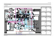
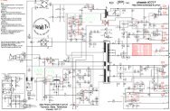
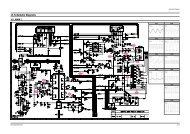
SERVICE MANUAL FOR M35&36; CHASSIS
SERVICE MANUAL FOR M35&36; CHASSIS
SERVICE MANUAL FOR M35&36; CHASSIS

Create successful ePaper yourself
Turn your PDF publications into a flip-book with our unique Google optimized e-Paper software.
TCL<br />
decay time: 37 ms<br />
Chassis M35&<strong>36</strong> Service Manual<br />
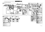
1.6. SCART Signal Routing<br />
1.6.1. SCART DSP In and SCART Out Select<br />
The SCART DSP Input Select and SCART Output Select blocks include full matrix switching facilities. To<br />
design a TV set with two pairs of SCART-inputs and one pair of SCART-outputs, no external switching<br />
hardware is required. The switches are controlled by the ACB user register.<br />
1.6.2. Stand-by Mode<br />
If the MSP 34x5G is switched off by first pulling STANDBYQ low and then (after >1⎧s delay) switching<br />
off DVSUP and AVSUP, but keeping AHVSUP<br />
(‘Stand-by’-mode), the SCART switches maintain their position and function. This allows the copying<br />
from selected SCART-inputs to SCART-outputs in the TV set’s stand-by mode.<br />
In case of power on or starting from stand-by (switching on the DVSUP and AVSUP, RESETQ going high<br />
2 ms later), all internal registers except the ACB register are reset to the default configuration .The reset position<br />
of the ACB register becomes active after the first I 2 C transmission into the Baseband Processing part. By<br />
transmitting the ACB register first, the reset state can be redefined.<br />
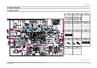
Pin Connections and Short Descriptions<br />
NC = not connected; leave vacant<br />
LV = if not used, leave vacant<br />
DVSS: if not used, connect to DVSS<br />
X = obligatory; connect as described in circuit diagram<br />
AHVSS: connect to AHVSS<br />
No. Pin Name Pin No. Type<br />
Connection<br />
(if not used)<br />
Short Description<br />
1 TP 1 LV Test pin<br />
2 NC 2 LV Not connected<br />
3 D_CTR_I/O_1 3 IN/OUT LV D_CTR_I/O_1<br />
4 D_CTR_I/O_0 4 IN/OUT LV D_CTR_I/O_0<br />
5 ADR_SEL 5 IN X I 2 C Bus address select<br />
6 STANDBYQ 6 IN X Standby (low-active)<br />
7 I2C_CL 7 IN/OUT X I 2 C clock<br />
8 I2C_DA 8 IN/OUT X I 2 C data<br />
9 I2C_CL 9 LV I 2 C clock<br />
10 I2C_WS 10 LV I 2 C word strobe<br />
11 I2C_DA_OUT 11 LV I 2 C data output<br />
12 I2C_DA_IN1 12 LV I 2 C data input<br />
13 ADR_DA 13 LV ADR data output<br />
14 ADR_WS 14 LV ADR word strobe<br />
15 ADR_CL 15 LV ADR clock<br />
16 DVSUP 16 X Digital power supply +5V<br />
17 DVSS 17 X Digital ground<br />
18 I2C_DA_IN2 18 LV I 2 C2-data input<br />
19 NC 19 LV Not connected<br />
20 RESETQ 20 IN X Power-on-reset<br />
21 NC 21 LV Not connected<br />
22 NC 22 LV Not connected<br />
23 VREF2 23 X<br />
Reference ground 2<br />
high-voltage part<br />
24 DACM_R 24 OUT LV Loudspeaker out, right<br />
25 DACM_L 25 OUT LV Loudspeaker out, left<br />
26 NC 26 LV Not connected<br />
27 NC 27 LV Not connected<br />
28 NC 28 LV Not connected<br />
31 03.Mar.2003