
Create successful ePaper yourself
Turn your PDF publications into a flip-book with our unique Google optimized e-Paper software.
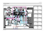
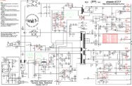
ST92195B - GENERAL INFORMATION<br />
PIN DESCRIPTION (Cont’d)<br />
RESET Reset (input, active low). The ST9+ is initialised<br />
by the Reset signal. With the deactivation<br />
of RESET, program execution begins from the<br />
Program memory location pointed to by the vector<br />
contained in program memory locations 00h and<br />
01h.<br />
R/G/B Red/Green/Blue. Video color analog DAC<br />
outputs.<br />
FB Fast Blanking. Video analog DAC output.<br />
VDD Main power supply voltage (5V10%, digital)<br />
WSCF, WSCR Analog pins for the VPS/WSS slicer<br />
line PLL (See note 1).<br />
MCFM Analog pin for the display pixel frequency<br />
multiplier.<br />
OSCIN, OSCOUT Oscillator (input and output).<br />
These pins connect a parallel-resonant crystal<br />
(24MHz maximum), or an external source to the<br />
on-chip clock oscillator and buffer. OSCIN is the<br />
input of the oscillator inverter and internal clock<br />
generator; OSCOUT is the output of the oscillator<br />
inverter.<br />
VSYNC Vertical Sync. Vertical video synchronisation<br />
input to OSD. Positive or negative polarity.<br />
HSYNC/CSYNC Horizontal/Composite sync. Horizontal<br />
or composite video synchronisation input to<br />
OSD. Positive or negative polarity.<br />
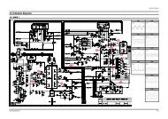
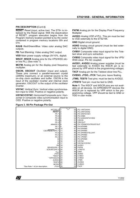
Figure 3. 56-Pin Package Pin-Out<br />
INT7/P2.0<br />
RESET<br />
P0.7<br />
P0.6<br />
P0.5<br />
P0.4<br />
P0.3<br />
AIN4/P0.2<br />
P0.1<br />
P0.0<br />
CSO/RESET0/P3.7<br />
P3.6<br />
P3.5<br />
P3.4<br />
B<br />
G<br />
R<br />
FB<br />
SDI/SDO/P5.1<br />
SCK/INT2/P5.0<br />
V DD<br />
JTDO<br />
*WSCF<br />
*VPP/WSCR<br />
AVDD3<br />
TEST0<br />
MCFM<br />
*See Note 1 of pin description. JTCK<br />
1<br />
2<br />
3<br />
4<br />
5<br />
6<br />
7<br />
8<br />
9<br />
10<br />
11<br />
12<br />
13<br />
14<br />
15<br />
16<br />
17<br />
18<br />
19<br />
20<br />
21<br />
22<br />
23<br />
24<br />
25<br />
26<br />
27<br />
28<br />
PXFM Analog pin for the Display Pixel Frequency<br />
Multiplier<br />
AVDD3 Analog VDD of PLL. This pin must be tied<br />
to VDD externally to the ST92195.<br />
GND Digital circuit ground.<br />
AGND Analog circuit ground (must be tied externally<br />
to digital GND).<br />
CVBS1 Composite video input signal for the Teletext<br />
slicer and sync extraction.<br />
CVBS2 Composite video input signal for the VPS/<br />
WSS slicer. Pin AC coupled.<br />
AVDD1, AVDD2 Analog power supplies (must be<br />
tied externally to AVDD3 the WSCR pin is replaced<br />
by VPP which is the programming voltage).<br />
TXCF Analog pin for the Teletext slicer line PLL.<br />
CVBSO, JTDO, JTCK Test pins: leave floating.<br />
JTMS, TEST0 Test pins: must be tied to AVDD2.<br />
JTRST0 Test pin: must be tied to GND.<br />
Note 1: The WSCF and WSCR pins are not available<br />
on all devices. On EPROM/OTP devices the<br />
WSCR pin is replaced by VPP which is the programming<br />
voltage. VPP should be tied to GND or<br />
VDD in user mode.<br />
56<br />
55<br />
54<br />
53<br />
52<br />
51<br />
50<br />
49<br />
48<br />
47<br />
46<br />
45<br />
44<br />
43<br />
42<br />
41<br />
40<br />
39<br />
38<br />
37<br />
36<br />
35<br />
34<br />
33<br />
32<br />
31<br />
30<br />
29<br />
P2.1/INT5/AIN1<br />
P2.2/INT0/AIN2<br />
P2.3/INT6/VS01<br />
P2.4/NMI<br />
P2.5/AIN3/INT4/VS02<br />
OSCIN<br />
OSCOUT<br />
P4.7/PWM7/EXTRG/STOUT<br />
P4.6/PWM6<br />
P4.5/PWM5<br />
P4.4/PWM4<br />
P4.3/PWM3/TSLU/HT<br />
P4.2/PWM2<br />
P4.1/PWM1<br />
P4.0/PWM0<br />
VSYNC<br />
HSYNC/CSYNC<br />
AVDD1<br />
PXFM<br />
JTRSTO<br />
GND<br />
AGND<br />
CVBS1<br />
CVBS2<br />
JTMS<br />
AVDD2<br />
CVBSO<br />
TXCF<br />
11/202