You also want an ePaper? Increase the reach of your titles
YUMPU automatically turns print PDFs into web optimized ePapers that Google loves.
<strong>SERVICE</strong> <strong>MANUAL</strong><br />
PT92 CHASSIS<br />
Modification reserved
PT-92 Chassis Service Manual<br />
CONTENTS<br />
PAGE<br />
1.Technical Data 4<br />
2. Recommendation for service repairs 5<br />
3. Handling of MOS chip components 5<br />
4. X-Ray radiation precaution 5<br />
5. Service Menu 6<br />
6. Specification of the connector (Euroscart) 9<br />
7. Component descriptions 10<br />
8. Block Diagrams 11<br />
9. Fault tracing diagram-power supply 14<br />
10. Power Supply circuit diagram 15<br />
11. Troubleshooting guide for main PCB 16<br />
12. Descriptions of the integrated circuits<br />
- TDA16846 SMPS IC 17<br />
- TDA935X UOC IC 21<br />
- TDA9875A TV SOUND IC (STEREO) 28<br />
- TDA9870A TV SOUND IC (G. STEREO) 35<br />
- TDA24C16 EEPROM 45<br />
- TDA8351 VERTICAL IC (110 O ) 47<br />
- TDA8356 VERTICAL IC (90 O ) 51<br />
- TDA2616 STEREO AUDIO AMPLIFIER (110 O ) 55<br />
- TDA2615 STEREO AUDIO AMPLIFIER (90 O ) 57<br />
- TDA7056 MONO AUDIO AMPLIFIER (90 O ) 60<br />
- TDA7057AQ HP AMPLIFIER 62<br />
- TDA7050 HP AMPLIFIER 64<br />
- TDA6107Q VIDEO OUTPUT AMPLIFIER 67<br />
- TCDT1100 OPTOCOUPLER 69<br />
- TDA9830 TV SOUND AM DEMODULATOR 71<br />
- SAA7710T DOLBY PRO LOGIC SURROUND 75<br />
- BU2508AF HORIZONTAL TRANSISTOR (110 O ) 80<br />
- BU508DF HORIZONTAL TRANSISTOR (90 O ) 83<br />
- SPP03N60S5 SMPS MOSFET (90 O ) 86<br />
- SPP04N60S5 SMPS MOSFET (110 O ) 88<br />
13. Dolby and secam L mono board and circuits diagrams 90<br />
14. Oscilloscope shapes 93<br />
3
PT-92 Chassis Service Manual<br />
TECHNICAL DATA<br />
CRT PANEL<br />
Visible Picture<br />
Deflection Angle<br />
Vertical Frequency<br />
Horizontal Frequency<br />
47” / 50 cm / 66 cm<br />
90 o / 110 o<br />
50Hz<br />
15.625Hz<br />
ELECTRONIC<br />
Program Number<br />
Teletext<br />
Tuner<br />
TV System<br />
Music Power<br />
100+AV<br />
Flof text<br />
Cable tuner - 8 MHz spacing for Hyper Band<br />
European CCIR system<br />
90 o 2x8 Watt Rms 10% distortion<br />
110 o 2x4 Watt Rms 10% distortion<br />
CONNECTIONS<br />
Euro AV Socket<br />
Include<br />
MAIN STAGE<br />
Mains Voltage<br />
Mains Frequency<br />
Power Consumption<br />
In Stby Mode<br />
165-260VAC<br />
50Hz<br />
110 o 126 W; 90 o 75 W<br />
110 o 8 W; 90 o 5 W<br />
4
PT-92 Chassis Service Manual<br />
RECOMMENDATION FOR <strong>SERVICE</strong> REPAIRS<br />
1- Use only original spare parts. Only use components<br />
with the same specifications for replacement.<br />
2- Original fuse value only should be used.<br />
3- Main leads and connecting leads should be checked<br />
for external damage before connection.<br />
Check the insulation.<br />
4- Parts contributing to the safety of the product must<br />
not be damaged or obviously unsuitable.<br />
This is valid especially for insulators and insulating<br />
parts.<br />
5- Thermally loaded solder pads are to be sucked off<br />
and re-soldered.<br />
6- Ensure that the ventilation slots are not obstructed.<br />
7- Potentials as high as 25 KV are present when this receiver<br />
is operating. Operation of the receiver<br />
outside the cabinet or with back cover removed involve<br />
a shock hazard from the receiver.<br />
Servicing should not be attempted by anyone who is<br />
not thoroughly familiar with the precautions<br />
necessary when working on high voltage equipment.<br />
Perfectly discharge the high potential of the picture<br />
tube before handling the tube. The picture tube is<br />
highly evacuated and if broken.<br />
Glass fragments will be violently expelled.<br />
Always discharge the picture tube anode to the receiver<br />
chassis to keep of the shock hazard before removing<br />
the anode cap.<br />
8- Keep wire away from the high voltage or high temperature<br />
components.<br />
9- When replacing a wattage resistor in circuit board,<br />
keep the resistor 10 mm away from circuit board.<br />
HANDLING OF MOS CHIP COMPONENTS<br />
MOS circuit requires special attention with regard to<br />
static charges. Static charges may occur with any highly<br />
insulating plastics and can be transferred to persons<br />
wearing clothes and shoes made of synthetic materials.<br />
Protective circuits on the inputs and outputs of mos<br />
circuits give protection to a limited extend only due to<br />
time of reaction.<br />
Please observe the following instructions to protect the<br />
components against damage from static charges.<br />
1- Keep mos components in conductive package until<br />
they are used. Most components must never be stored<br />
in styropor materials or plastic magazines.<br />
2- Persons have to rid themselves of electrostatic charges<br />
by touching MOS components.<br />
3- Hold the component by the body touching the terminals.<br />
4- Use only grounded instruments for testing and processing<br />
purposes.<br />
5- Remove or connect MOS ICs when operating voltage<br />
is disconnected.<br />
X-RAY RADIATION PRECAUTION<br />
1- Excessive high voltage can be produce potentially<br />
hazardous X-RAY radiation. To avoid such hazard,<br />
the high voltage must not be above the specified limit.<br />
The nominal value of the high voltage of this receiver<br />
is 25KV at zero beam current (minimum<br />
brightness) under 220V AC power source. The high<br />
voltage must not under any circumstance, exceed<br />
30KV. It is recommended the reading of the high voltage<br />
be recorded as a part of the service record. It is<br />
important to use an accurate and reliable high voltage<br />
meter.<br />
2- The primary source of X-RAY radiation in this TV receiver<br />
is the picture tube. For continued X-RAY radiation<br />
protection, the replacement tube must be<br />
exactly the same type tube as specified in the part<br />
list.<br />
5
PT-92 Chassis Service Manual<br />
<strong>SERVICE</strong> MENU<br />
The service menu is entered by pressing the key on the RC and VOLUME-DOWN key on the TV simultaneously<br />
when the TV is in TV- mode. The service menu is left by pressing the key.<br />
When entering the service mode the first menu item is IF (selection of normal IF). Next items can be selected using the keys<br />
and . The value of each item can be changed using the keys and<br />
. The item values are displayed as decimal values, except for the tuner-band-selection, BITS and option<br />
items.<br />
They are displayed as hexa-decimal values. All values are stored in non-volatile memory when the service menu is left. The<br />
“INIT CTV832U” item initializes the NVM: It clears all names and tuning information of all programs and writes default values<br />
for the service alignments and preset values in NVM. While doing so, the OSD displays “BUSY”. When the initialization is<br />
finished, the message “READY” is written on the screen.<br />
Item DefauIt Explanation<br />
IF 38.9 IF selection (58.8, 45.8, 38.9 or 38.00 MHz)<br />
IFL1 33.9 IF for SECAM-L1 selection (33.4 or 33.9 MHz)<br />
HP 31 Horizontal parallelogram<br />
HB 31 Horizontal bow<br />
EW 37 East-west Width for picture setting 16:9<br />
PW 18 East-west Parabola for picture setting 16:9<br />
UCP 13 East-west Upper Corner parabola for picture setting 16:9<br />
LCP 13 East-west Lower Corner parabola for picture setting 16:9<br />
TC 28 East-west Trapezium for picture setting 16:9<br />
HP4:3 31 Horizontal parallelogram for picture setting 4:3<br />
HB4:3 31 Horizontal bow for picture setting 4:3<br />
EW4:3 45 East-west Width for picture setting 4:3<br />
PW4:3 15 East-west Parabola for picture setting 4:3<br />
UCP4:3 35 East-west Upper Corner parabola for picture setting 4:3<br />
LCP4:3 25 East-west Lower Corner parabola for picture setting 4:3<br />
TC4:3 31 East-west Trapezium for picture setting 4:3<br />
HS 31 Horizontal Shift<br />
VS 31 Vertical Slope<br />
VA 31 Vertical Amplitude<br />
SC 31 S-Correction<br />
VSD off Vertical Scan Disable<br />
VSH 31 Vertical Shift<br />
VX 25 Vertical zoom (East-west only)<br />
BLR 7 Black Level Red<br />
BLG 7 Black Level Green<br />
WPR 31 White point correction Red<br />
WPG 31 White point correction Green<br />
WPB 31 White point correction Blue<br />
Ys 15 Y-delay adjustment for SECAM<br />
Yn 8 Y-delay adjustment for NTSC<br />
YP 0 Y-delay adjustment for PAL<br />
6
PT-92 Chassis Service Manual<br />
Yo 0 Y-delay adjustment for external sources<br />
AGC 4 AGC take over<br />
CL 4 Cathode drive level<br />
Bits 00 (ACL=0; FCO= 0; SVO= 0; HP2= 0; FSL= 0; OSO= 0)<br />
Bits1 00 (FFI= 0; TV= 0; AV-1= 0; AV-2= 0; AV-2S= 0;<br />
AV-3= 0; AV-3S= 0; AV = 0)<br />
OptByte1<br />
(Default=E3)<br />
PAL-BG = Selection PAL-BG (1)<br />
PAL-DK = Selection PAL-DK (1)<br />
PAL-I = Selection PAL-I (0)<br />
PAL-M = Selection PAL-M (0)<br />
PAL-N = Selection PAL-N (0)<br />
NTSC-M = Selection NTSC-M (1)<br />
NTSC-443 = Selection NTSC-443 (1)<br />
SECAM-BG = Selection SECAM-BG (1)<br />
*(1) Selected, (0) Not Selected<br />
OptByte2<br />
(Default=07)<br />
SECAM-DK = Selection SECAM-DK (1)<br />
FRANCE = Selection FRANCE (1)<br />
WEB = Enable/Disable (1/0)<br />
PalBG Scr = When the PalBG Scr selected, TV searches only<br />
PalBG. Otherwise it searches all. (0)<br />
AV2 = Selection AV2 (0)<br />
*(1) Selected, (0) Not Selected<br />
OptByte3<br />
(Default=E8)<br />
= (0)<br />
JR = (0)<br />
HP = (0)<br />
Vol Bar = (1)<br />
Sub Wof = (0)<br />
Presets = (1)<br />
Lock = (1)<br />
Hotel = (0)<br />
When the Hotel mode selected, It’s impossible to<br />
nter menu settings.lt selects the Hotel mode. (1)<br />
*(1) Selected, (0) Not Selected<br />
OptByte4<br />
(Default=B8)<br />
16:9 = Set 16:9 mode active (1)<br />
110 = Selection 110/90 Tube (1/0)<br />
Hpol = Default (0)<br />
Vpol = DefauIt (0)<br />
Field = Default (1)<br />
FE-Out = Default (1)<br />
Sw-on = When the power on the TV, it Enables or Disables<br />
Standby Mode. (1/0)<br />
Vg-Check = Default (1)<br />
*(1) Selected, (0) Not Selected<br />
OptByte5<br />
(Default=09)<br />
Clock = Enable/Disable Clock Menu (1)<br />
AM/PM = (1)<br />
AVL = Auto Volume Level (1)<br />
= (0)<br />
1-norma = Default (0)<br />
Flof-Txt = (0)<br />
TR = (0)<br />
DVD Start = (0)<br />
*(1) Selected, (0) Not Selected<br />
7
PT-92 Chassis Service Manual<br />
OptByte6<br />
(Default=00)<br />
UOC-J = Default (0)<br />
ignrSUP = Default (0)<br />
ignrNDF = Default (0)<br />
Pal-BG/DK = (0)<br />
Pal-L = (0)<br />
Eco = (0)<br />
WEB ST = (0)<br />
WSS = (0)<br />
TSL 45 Start frequency of the low-band in MHz<br />
TEL 118 End frequency of the low-band<br />
TSM 118 Start frequency of the mid-band<br />
TEM 400 End frequency of the mid-band<br />
TSH 400 Start frequency of the high-band<br />
TEH 863 End frequency of the high-band<br />
TBL 03 hex Value needed for switching to the low-band<br />
TBN 06 hex Value needed for switching to the mid-band<br />
TBH 85 hex Value needed for switching to the high-band<br />
16:9 / 4:3 Adjustment<br />
The CTV832U software uses two sets of parameters for the registers HP (horizontal parallelogram), HB (horizontal<br />
bow), EW (EW width), PW (parabola/width), UCP (upper corner parabola), LCP (lower corner parabola)<br />
and IC (EW trapezium). They occur in the service menu for 16:9 screen with the listed abbreviations.<br />
For the 4:3 screen there is a second set of these registers. They occur in the service menu with the extension ‘4:3’<br />
(i.e. HP4:3, HB4:3,...).<br />
Each register set must be adjusted under the right conditions i.e. the 16:9 settings are adjusted with a 16:9 picture -<br />
the 4:3 settings with a 4:3 picture.<br />
The inenu items EW, PW, UCP, LCP, TC, HP4:3, HB4:3,... TC4:3 and VX will only be in the service menu if the<br />
option 16:9 is set in 4 th option byte.<br />
TUNER PARAMETER IN <strong>SERVICE</strong> AND DEFINITION PHILIPS OREGA TEMIC SAMSUNG ALPS<br />
TSL Start frequency of the low-band in MHz 45 45 45 45 45<br />
TEL End frequency of the low-band 160 118 150 150 180<br />
TSM Start frequency of the mid-band 160 118 150 150 180<br />
TEM End frequency of the mid-band 440 400 440 425 465<br />
TSH Start frequency of the high-band 440 400 440 425 465<br />
TEH End frequency of the high-band 863 865 865 865 900<br />
TBL hex Value needed for switching to the low-band A1 03 01 01 01<br />
TBN hex Value needed for switching to the mid-band 92 06 02 02 02<br />
TBH hex Value needed for switching to the high-band 34 85 04 08 0C<br />
8
PT-92 Chassis Service Manual<br />
SPECIFICATIONS OF THE CONNECTOR<br />
(EURO SCART)<br />
I- Audio output 1. right channel 0.5 VRMS/10k 0<br />
7- RGB input, blue (B)<br />
8- Switch signal video (status)<br />
9- GND<br />
10- Reserved for clock signals (not connected)<br />
11- RGB input, green (G)<br />
12- Reserved for remote control (not connected)<br />
13- GND<br />
14- GND switch signal RGB<br />
15- RGB input, red (R)<br />
16- Switch signal RGB<br />
17- GND (video)<br />
18- GND19- Video output 1 Vpp/75 ohm<br />
20- Video input 1 Vpp/75 ohm<br />
21- Shield<br />
1 3 5 7 9 11 13 15 17 19 21<br />
2 4 6 8 10 12 14 16 18 20<br />
9
PT-92 Chassis Service Manual<br />
POWER CORD<br />
SAW FILTER<br />
IR SENSOR<br />
VOLTAGE REGULATOR<br />
ON/OFF SWITCH<br />
COMPONENT DESCRIPTIONS<br />
LINE FILTER<br />
PTC<br />
NPN TRANSISTOR<br />
PNP TRANSISTOR<br />
CERAMIC FILTER<br />
COIL<br />
LINEARITY COIL<br />
FUSIBLE RESISTOR<br />
IW METAL OXIDE RESISTOR<br />
1/2W METAL OXIDE RESISTOR<br />
1/4 OR 1/6W CARBON FILM RESISTOR<br />
CERAMIC CAPACITOR /POLYESTER CAPACITOR<br />
ELECTROLYTIC CAPACITOR<br />
DIODE<br />
ZENER DIODE<br />
SWITCH JUMPER<br />
NET (INPUT)<br />
NET (OUTPUT)<br />
TACT SWITCH<br />
10 10
PT-92 Chassis Service Manual<br />
PT92 110 o STEREO CHASSIS<br />
AGC<br />
UV1316 PLL<br />
Tuner<br />
I 2 C<br />
STEREO<br />
I 2 C<br />
Scarts<br />
L/R<br />
TDA9870A/75A<br />
Sound Processor<br />
TDA2616<br />
Sound<br />
Amplifier<br />
L<br />
R<br />
SAV<br />
Filter<br />
Sub<br />
IF<br />
RGB<br />
TDA6107Q<br />
Externals<br />
Sound<br />
Trap<br />
L/R<br />
TDA935X/6X/8X<br />
PAL/SECAM/NTSC<br />
TV Signal Proc.<br />
Teletext Decoder<br />
µ-Controller<br />
RGB Processing<br />
Iblack<br />
Vdrive<br />
Guard<br />
Beam<br />
Current<br />
Triple RGB<br />
Output Amplifier<br />
TDA8351<br />
DC Vertical<br />
Amplifier<br />
BU2525AF<br />
Ver.<br />
Hor.<br />
110 o<br />
CVBS<br />
Hdrive<br />
Flyback<br />
Horizontal<br />
Deflection<br />
& EHT<br />
EHT<br />
E/W (110 o )<br />
RGB<br />
12.000<br />
Supply<br />
Degaussing<br />
PCA8521<br />
RC-5 Transmitter<br />
I 2 C<br />
16K<br />
EEPROM<br />
TDA16846<br />
SMPS<br />
Mains<br />
≈ 220<br />
11
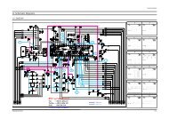
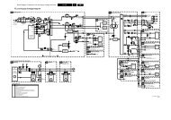
PT-92 Chassis Service Manual<br />
PT92 90 o STEREO CHASSIS<br />
12
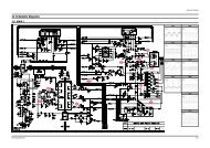
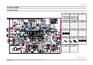
PT-92 Chassis Service Manual<br />
PT92 90 o MONO CHASSIS<br />
13
PT-92 Chassis Service Manual<br />
FAULT TRACING DIAGRAM-POWER SUPPLY<br />
Switched mode power<br />
supply defective,+145V<br />
is missing or level is wrong<br />
DP 01 ÷ 04<br />
CP 01 ÷ 04<br />
CP 06, TP01<br />
YES<br />
Fuse<br />
F1 defective<br />
NO<br />
RP 07, RP 05<br />
open and<br />
short circuit<br />
NO<br />
Voltage at drain<br />
TP 01<br />
YES<br />
RP 06<br />
YES<br />
Voltage at<br />
IP 01<br />
PIN 11<br />
< 1V<br />
NO<br />
RP 11, DP 07<br />
YES<br />
Start-up voltage<br />
(6)<br />
PIN 14<br />
< 8V<br />
NO<br />
TP 01<br />
YES<br />
Start-up voltage<br />
varies ca. 8V<br />
IP 01<br />
NO<br />
Measure +145 V<br />
VAP 1, RP 03<br />
NO<br />
+145V<br />
adjustable with<br />
VAP 01<br />
YES<br />
Control range of<br />
switched-mode<br />
power supply<br />
14
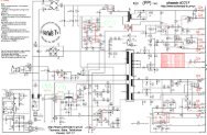
PT-92 Chassis Service Manual<br />
POWER SUPPLY<br />
15
PT-92 Chassis Service Manual<br />
TROUBLESHOOTING GUIDE FOR MAIN PCB<br />
TROUBLE<br />
CHECK POINTS<br />
No color<br />
Horizontal linearity<br />
Horizontal size<br />
Flue picture<br />
Dark picture<br />
Noise picture<br />
Interference<br />
No sound<br />
Sound distortion<br />
Memory<br />
No video on the SCART<br />
No audio on the SCART<br />
No picture<br />
CV37, CV38, XV01<br />
LD02, RD20, DD06<br />
+B voltage, CD18, CD20, CD27, CD08, TV06<br />
RD17, RD06, RD62, R001, Focus adjust<br />
Screen adjust, EHT voltage<br />
TU01, AGC adjust, If adjust<br />
TV01, TV04, TU01<br />
IA50, IA51, IA01, DP17, DP12, RA51, X301, I302, IV01<br />
I302, IC01, L304, CA07, CA06, RA06, RA07, IA01, IA50, IA51<br />
IC02, IV01, TC10<br />
IV01, TE01, TE04<br />
I302, TV03<br />
TD01, TD02, DD01, TD04, DD03, DD04, ID50, RD56, IV01<br />
16
PT-92 Chassis Service Manual<br />
TDA16846<br />
Controller For Switch Mode Power Supplies<br />
The TDA16846 is suited for TV-, VCR-sets and SAT receivers. It also can be good used in PC monitors.<br />
The TDA 16847 is identical with TDA16846 but has an additional power measurement output (pin 8) which can be used<br />
a Temporary High Power Circuit.<br />
Pin Configuration (top view)<br />
DTC<br />
1<br />
U<br />
14<br />
VCC<br />
PCS<br />
2<br />
13<br />
OUT<br />
RZI<br />
3<br />
12<br />
GND<br />
SRC<br />
4<br />
11<br />
PVC<br />
OCI<br />
5<br />
10<br />
FC1<br />
FC2<br />
6<br />
9<br />
REF<br />
SYN<br />
7<br />
8<br />
N.C./PMO<br />
Pin Definitions and Functions<br />
Pin Symbol Function<br />
1 OTC Off Time Circuit<br />
2 PCS Primary Current Simulation<br />
3 RZI Regulation and Zero Crossing Input<br />
4 SRC Soft-Start and Regulation Capacitor<br />
5 OCI Opto Coupler Input<br />
6 FC2 Fault Comparator 2<br />
7 SYN Synchronization Input<br />
8 N.C./PMO Not Connected (TDA16846)<br />
9 REF Reference Voltage and Current<br />
10 FC1 Fault Comparator 1<br />
11 PVC Primary Voltage Check<br />
12 GND Ground<br />
13 OUT Output<br />
14 VCC Supply Voltage<br />
17
PT-92 Chassis Service Manual<br />
TDA16846 Block Diagrams<br />
SYN<br />
OTC<br />
RZI<br />
SRC<br />
OCI<br />
PCS<br />
V CC<br />
GND<br />
D 4<br />
R 4<br />
Fold Back Point Correction<br />
11<br />
R 6 x1/3<br />
Primary<br />
KSY<br />
Voltage<br />
R ∞<br />
7 -<br />
PVA<br />
Check<br />
R 6 D5<br />
5V<br />
+<br />
∞<br />
∞<br />
30kΩ<br />
-<br />
-<br />
1V<br />
R 3<br />
+<br />
+<br />
R<br />
1.5V<br />
8<br />
75kΩ 15kΩ<br />
Control Voltage<br />
–<br />
Off Time<br />
3.5V<br />
G1<br />
V CC<br />
Limit Comparator<br />
+<br />
1<br />
5V ∞<br />
+<br />
ED2<br />
1<br />
-<br />
CS1<br />
RSTC/RSTF<br />
G4<br />
∞<br />
1<br />
+<br />
Eror<br />
3.5V<br />
–<br />
5V Amplifier R 2<br />
Error-<br />
D 2<br />
Flipflop<br />
∞<br />
FC2<br />
3<br />
+ S<br />
- Q<br />
R<br />
D 3<br />
Buffer for<br />
Control Voltage<br />
4<br />
5<br />
+ ∞<br />
-<br />
R 1<br />
Output<br />
On Time<br />
&<br />
G3 Driver<br />
20kΩ Comparator<br />
S<br />
&<br />
∞<br />
2 5V<br />
G2<br />
Q<br />
-<br />
R<br />
+<br />
I 1<br />
ED1<br />
Zero Crossing<br />
1.5V<br />
Signal<br />
D1<br />
PT-92 Chassis Service Manual<br />
ELECTRICAL CHARACTERISTICS<br />
Absolute maximum ratings<br />
All voltages listed are referenced to ground (0V, Vss) except where noted.<br />
Parameter Symbol Limit Values Unit Remarks<br />
Min. Typ.<br />
Supply Voltage at Pin 14 V cc -0.3 17 V -<br />
Voltage at Pin 1, 4, 5, 6, 7, 9, 10 - -0.3 6 V -<br />
Voltage at Pin 2, 8, 11 - -0.3 17 V -<br />
Voltage at Pin 3 RZI 6 V -<br />
Current into Pin 3 -10 mA V 3 < - 0.3V<br />
Current into Pin 9 REF -1 - mA -<br />
Current into Pin 13 OUT 100 mA V 13 > - V cc<br />
-100 mA V 13 < - 0V<br />
ESD Protection - - 2 kV MIIL STD 883C<br />
methot 3015.6,<br />
100 PF, 1500Ω<br />
Storage Temperature T stg -65 125 o<br />
C -<br />
Operating Junction Temperature T j - 125 o<br />
C -<br />
Thermal Resistance R thJA - 110 K/W P-DIP-14-3<br />
Junction-Ambient<br />
Soldering Temperature - - 260 o<br />
C -<br />
Soldering Time - - 10 s -<br />
Note: Stresses above those listed here may cause permanent damage to the device. Exposure to absolute<br />
maximum rating conditions for extended periods may affect device reliability.<br />
19
PT-92 Chassis Service Manual<br />
Short Description of the Pin Functions<br />
Pin<br />
Functions<br />
1 A parallel RC-circuit between this pin and ground determines the ringing suppression time<br />
and the standby-frequency.<br />
2 A capacitor between this pin and ground and a resistor between this pin and the positive<br />
terminal of the primary elcap quantifies the max. possible output power of the SMPS.<br />
3 This is the input of the error amplifier and the zero crossing input. The output of a voltage<br />
divider between the control winding and ground is connected to this input. If the pulses at<br />
pin 3 exceed a 5 V threshold, the control voltage at pin 4 is lowered.<br />
4 This is the pin for the control voltage. A capacitor has to be connected between this pin<br />
and ground. The value of this capacitor determines the duration of the softstart and the<br />
speed of the control.<br />
5 If an opto coupler for the control is used, it's output has to be connected between this pin<br />
and ground. The voltage divider at pin 3 has then to be changed, so that the pulses at pin<br />
3 are below 5 V.<br />
6 Fault comparator 2: If a voltage > 1.2 V is applied to this pin, the SMPS stops.<br />
7 If fixed frequency mode is wanted, a parallel RC circuit has to be connected between this<br />
pin and ground. The RC-value determines the frequency. If synchronized mode is wanted,<br />
sync pulses have to be fed into this pin.<br />
8 Not connected (TDA16846). / This is the power measurement output of the Temporary<br />
High Power Circuit. A capacitor and a RC-circuit has to be connected between this pin<br />
and ground.<br />
9 Output for reference voltage (5 V). With a resistor between this pin and ground the fault<br />
comparator 2 (pin 6) is enabled.<br />
10 Fault comparator i: If a voltage > 1 V is applied to this pin, the SMPS stops.<br />
11 This is the input of the primary voltage check. The voltage at the anode of the primary<br />
elcap has to be fed to this pin via a voltage divider. If the voltage of this pin falls below<br />
1 V, the SMPS is switched off. A second function of this pin is the primary voltage dependent<br />
fold back point correction (only active in free running mode).<br />
12 Common ground.<br />
13 Output signal. This pin has to be connected across a serial resistor with the gate of the<br />
power transistor.<br />
14 Connection for supply voltage and startup capacitor. After startup the supply voltage is<br />
produced by the control winding of the transformer and rectified by an external diode.<br />
20
PT-92 Chassis Service Manual<br />
TDA935X/6X/8X<br />
TV signal processor-Teletext decoder with embedded µ-Controller<br />
GENERAL DESCRIPTION<br />
The various versions of the TDA935X/6X/8X series<br />
combine the functions of a n/ signal processor together<br />
with a µ-Controller and US Closed Caption decoder.<br />
Most versions have a Teletext decoder on board.<br />
The Teletext decoder has an internal RAM memory<br />
for 1 or 10 page text. The ICs are intended to be<br />
used in economy television receivers with 90 o and<br />
110 o picture tubes.<br />
The ICs have supply voltages of 8 V and 3.3 V and<br />
they are mounted in S-DIP envelope with 64 pins.<br />
The features are given in the following feature list.<br />
The differences between the various ICs are given in<br />
the table on page 4.<br />
FEATURES<br />
TV-signal processor<br />
• Multi-standard vision IF circuit with alignment-free PLL<br />
demodulator<br />
• Internal (switchable) time-constant for the IF-AGC circuit<br />
• A choice can be made between versions with mono<br />
intercarrier sound FM demodulator and versions with<br />
QSS IF amplifier.<br />
• The mono intercarrier sound versions have a selective<br />
FM-PLL demodulator which can be switched to the<br />
different FM sound frequencies (4.5/5.5/6.0/6.5 MHz).<br />
The quality of this system is such that the external<br />
band-pass filters can be omitted.<br />
• Source selection between 'internal’ CVBS and external<br />
CVBS or Y/C signals<br />
• Integrated chrominance trap circuit<br />
• Integrated luminance delay line with adjustable delay<br />
time<br />
• Asymmetrical ‘delay line type’ peaking in the luminance<br />
channel<br />
• Black stretching for non-standard luminance signals<br />
• Integrated chroma band-pass filter with switchable<br />
centre frequency<br />
• Only one reference (12 MHz) crystal required for the<br />
CL-Controller, Teletext- and the colour decoder<br />
• PAL/NTSC or multi-standard colour decoder with<br />
automatic search system<br />
• Internal base-band delay line<br />
• RGB control circuit with ‘Continuous Cathode<br />
Calibration’, white point and black level off set<br />
adjustment so that the colour temperature of the dark<br />
and the light parts of the screen can be chosen<br />
independently.<br />
• Linear RGB or YUV input with fast blanking for external<br />
RGB/YUV sources. The Text/OSD signals are internally<br />
supplied from the µ-Controller/Teletext decoder<br />
• Contrast reduction possibility during mixed-mode of<br />
OSD and Text signals<br />
• Horizontal synchronization with two control loops and<br />
alignment-free horizontal oscillator<br />
• Vertical count-down circuit<br />
• Vertical driver optimized for DC-coupled vertical output<br />
stages<br />
• Horizontal and vertical geometry processing<br />
• Horizontal and vertical zoom function for 16 : 9<br />
applications<br />
• Horizontal parallelogram and bow correction for large<br />
screen picture tubes<br />
21
PT-92 Chassis Service Manual<br />
µ-CONTROLLER<br />
• 80C51 µ-controller core standard instruction set and<br />
timing<br />
• 1 µs machine cycle<br />
• 32 - 128Kx8-bit late programmed ROM<br />
• 3 - 12Kx8-bit Auxiliary RAM (shared with Display and<br />
Acquisition)<br />
• Interrupt controller for individual enable/disable with<br />
two level priority<br />
• Two 16-bit Timer/Counter registers<br />
• WatchDog timer<br />
• Auxiliary RAM page pointer<br />
• 16-bit Data pointer<br />
• IDLE and Power Down (PD) mode<br />
• 14 bits PWM for Voltage Synthesis Tuning<br />
• 8-bit A/D converter<br />
• 4 pins which can be programmed as general<br />
I/O pin, ADC input or PWM (6-bit) output<br />
DATA CAPTURE<br />
• Text memory for 1 or 10 pages<br />
• In the 10 page versions inventory of transmitted<br />
Teletext pages stored in the Transmitted Page Table<br />
(TPT) and Subtitle Page Table (SPT)<br />
• Data Capture for US Closed Caption<br />
• Data Capture for 525/625 line WST, VPS<br />
(PDC system A) and Wise Screen Signalling (WSS)<br />
bit decoding<br />
• Automatic selection between 525 WST/625 WST<br />
• Automatic selection between 625 WST/VPS on line<br />
16 of VBI<br />
• Real-time capture and decoding for WST Teletext in<br />
Hardware, to enable optimized µ-processor throughput<br />
• Automatic detection of FASTEXT transmission<br />
• Real-time packet 26 engine in Hardware for processing<br />
accented, G2 and G3 characters<br />
• Signal quality detector for video and WST/VPS data<br />
types<br />
• Comprehensive teletext language coverage<br />
• Full Field and Vertical Blanking Interval (VBI) data<br />
capture of WST data<br />
DISPLAY<br />
• Teletext and Enhanced OSD modes<br />
• Features of level 1.5 WST and US Close Caption<br />
• Serial and Parallel Display Attributes<br />
• Single/Double/Quadruple Width and Height for<br />
characters<br />
• Scrolling of display region<br />
• Variable flash rate controlled by software<br />
• Enhanced display features including overlining,<br />
underlining and italics<br />
• Soft colours using CLUT with 4096 colour palette<br />
• Globally selectable scan lines per row (9/10/13/16)<br />
and character matrix [12x10, 12x13, 12x16 (VxH)]<br />
• Fringing (Shadow) selectable from N-S-E-W direction<br />
• Fringe colour selectable<br />
• Meshing of defined area<br />
• Contrast reduction of defined area<br />
• Cursor<br />
• Special Graphics Characters with two planes,<br />
allowing four colours per character<br />
• 32 software redefinable On-Screen display characters<br />
• 4 WST Character sets (GO/G2) in single device (e.g.<br />
Latin, Cyrillic, Greek, Arabic)<br />
• G1 Mosaic graphics, Limited G3 Line drawing<br />
characters<br />
• WST Character sets and Closed Caption Character<br />
set in single device.<br />
22
PT-92 Chassis Service Manual<br />
Block Diagram<br />
23
PT-92 Chassis Service Manual<br />
QUICK REFERENCE DATA<br />
SYMBOL PARAMETER Min. Typ. Max. Unit<br />
Supply<br />
V P supply voltage - 8.0/3.3 - V<br />
I p supply current - tbf - mA<br />
Input voltages<br />
V iSIF(rms) video IF amplifier sensitivity (RMS value) - 35 - µV<br />
V iVIF(rms) QSS sound IF amplifier sensitivity (RMS value) - 60 - µV<br />
V iAUDIO(rms) external audio input (RMS value) - 500 - mV<br />
V iCVBS(p-p) external CVBS/Y input (peak-to-peak value) - 1.0 - V<br />
V iCHORAMA(p-p) external chroma input voltage (burst amplitude) - 0.3 - V<br />
(peak-to-peak value)<br />
V iRGB(p-p) RGB inputs (peak-to-peak value) - 0.7 - V<br />
V iYIN(p-p) luminance input signal (peak-to-peak value) - 1.4 - V<br />
V iUVIN(p-p) U/V input signal (peak-to-peak value) - 1.33/1.05 - V<br />
Output signals<br />
V o(IFVO(p-p) demodulated CVBS output (peak-to-peak value) - 2.5 - V<br />
V o(QSSO)(rms) sound IF intercarrier output in QSS versions (RMS value) - 100 - mV<br />
V o(AMOUT)(rms) demodulated AM sound output in QSS versions (RMS value) - 500 - mV<br />
I o(AGCOUT) tuner AGC output current range 0 - 5 mV<br />
V oRGB(p-p) RGB output signal amplitudes (peak-to-peak value) - 2.0 - V<br />
I o HOUT horizontal output current 10 - - mA<br />
I o VERT vertical output current (peak-to-peak value) 1 - - mA<br />
I o EWD EW drive output current 1.2 - - mA<br />
24
PT-92 Chassis Service Manual<br />
PINNING<br />
SYMBOL PIN DESCRIPTION<br />
P1.3TT1 1 port 1.3 or Counter/Timer 1 input<br />
P1.6/SCL 2 port 1.6 or I 2 C-bus clock line<br />
P1.7/SDA 3 port 1.7 or I 2 C-bus data line<br />
P2. O/TPWM 4 port 2.0 or Tuning PWM output<br />
P3.0/ADC0 5 port 3.0 or ADC0 input<br />
P3.1/ADCI 6 port 3.1 or ADC1 input<br />
P3.2/ADC2 7 port 3.2 or ADC2 input<br />
P3.3/ADC3 8 port 3.3 or ADC3 input<br />
VSSC/P 9 digital ground for µ-Controller core and periphery<br />
P0.5 10 port 0.5 (8 mA current sinking capability for direct drive of LEDs)<br />
P0.6 11 port 0.6 (8 mA current sinking capability for direct drive of LEDs)<br />
VSSA 12 analog ground of Teletext decoder and digital ground of TV- processor<br />
SECPLL 13 SECAM PLL decoupling<br />
VP2 14 2 nd supply voltage TV-processor (+8V)<br />
DECDIG 15 decoupling digital supply of TV-processor<br />
PH2LF 16 phase-2 filter<br />
PH1LF 17 phase-1 filter<br />
GND3 18 ground 3 for TV-processor<br />
DECBG 19 bandgap decoupling<br />
AVL/EWD (1) 20 Automatic Volume Levelling /East-West drive output<br />
VDRB 21 vertical drive B output<br />
VDRA 22 vertical drive A output<br />
IFIN1 23 IF input 1<br />
IFIN2 24 IF input 2<br />
IREF 25 reference current input<br />
VSC 26 vertical sawtooth capacitor<br />
TUNERAGC 27 tuner AGC output<br />
AUDEEM/SIFIN1 (1) 28 audio deemphasis or SIF input 1<br />
DECSDEM/SIFIN2 (1) 29 decoupling sound demodulator or SIF input 2<br />
GND2 30 ground 2 for TV-processor<br />
SNDPLL/SIFAGC (1) 31 narrow band PLL filter / AGC sound IF<br />
AVL/REF0/AMOUT (1) 32 Automatic Volume Levelling / subcarrier reference output/AM output (non controlled)<br />
HOUT 33 horizontal output<br />
FBISO 34 flyback input/sandcastle output<br />
AUDEXT/ 35 external audio input/QSS intercarrier out /AM audio output (non controlled)<br />
QSSO/AMOUT (1)<br />
EHTO 36 EHT/overvoltage protection input<br />
PLLIF 37 IF-PLL loop filter<br />
IFVO/SVO 38 IF video output / selected CVBS output<br />
VP1 39 main supply voltage TV-processor (+8 V)<br />
CVBSINT 40 internal CVBS input<br />
25
PT-92 Chassis Service Manual<br />
PINNING<br />
SYMBOL PIN DESCRIPTION<br />
GND1 41 ground 1 for TV-processor<br />
CVBS/Y 42 external CVBS/Y input<br />
CHROMA 43 chrominance input (SVHS)<br />
AUDOUT / AMOUT (1) 44 audio output / AM audio output (volume controlled)<br />
INSSW2 45 2 nd RGB /YUV insertion input<br />
R2/VIN 46 2 nd R input / V (R-Y) input<br />
G2 YIN 47 2 nd G input Y input<br />
B2 UIN 48 2 nd B input / U (B-Y) input<br />
BCLIN 49 beam current limiter input/V-guard input<br />
BLKIN 50 black current input<br />
RO 51 Red output<br />
GO 52 Green output<br />
BO 53 Blue output<br />
VDDA 54 analog supply of Teletext decoder and digital supply of TV-processor (3.3 V)<br />
VPE 55 OTP Programming Voltage<br />
VDDC 56 digital supply to core (3.3V)<br />
OSCGND 57 oscillator ground supply<br />
XTALIN 58 crystal oscillator input<br />
XTALOUT 59 crystal oscillator output<br />
RESET 60 reset<br />
VDDP 61 digital supply to periphery (+3.3 V)<br />
P1.0/INT1 62 port 1.0 or external interrupt 1 input<br />
P1.1/T0 63 port 1.1 or Counter/Timer 0 input<br />
P1.2/INT0 64 port 1.2 or external interrupt 0 input<br />
Note<br />
1. The function of pin 20, 28, 29, 31, 32, 35 and 44 is dependent on the IC version (mono irtercarrier FM demodulator / QSS IF<br />
amplifier and East-West output or not) and on some software control bits. The valid combinations are given in table 1.<br />
Table 1 Pin functions for various versions<br />
IC version FM-PLL version QSS version<br />
East-West Y/N N Y N Y<br />
CMB1/CMB0 bits - 00 01/10/11 00 01/10/11 00 01/10/11<br />
AM bit - - - - 0 1 - 0 1<br />
Pin 20 AVL EWD AVL EWD<br />
Pin 28 AUDEEM SIFIN1<br />
Pin 29 DECSDEM SIFIN2<br />
Pin 31 SNDPLL SIFAGC<br />
Pin 32 REFO AVL REFO AMOUT REFO AMOUT REFO<br />
Pin 35 AUDEXT AUDEX QSSO AMOUT AUDEXT QSSO AMOUT<br />
Pin 44 AUDOUT controlled AM out<br />
26
PT-92 Chassis Service Manual<br />
Pin configuration (SDIP 64)<br />
P1.3TT1<br />
P1.G/SCL<br />
P1.7/SDA<br />
P2.0TPMW<br />
P3.0/ADC0<br />
P3.1/ADC1<br />
P3.2/ADC2<br />
P3.3/ADC3<br />
VSSC/P<br />
U<br />
1 64<br />
2 63<br />
3 62<br />
4 61<br />
5 60<br />
6 59<br />
7 58<br />
8 57<br />
9 56<br />
P1.2/ONTO<br />
P1.1/TO<br />
P1.0/INT1<br />
VDDP<br />
RESET<br />
XTALOUT<br />
XTALIN<br />
OSCGND<br />
VDDC<br />
P0.5 10 55 VPE<br />
P0.6 11 54 VDDA<br />
VSSA<br />
SECPLL<br />
VP2<br />
DECDIG<br />
PH2LF<br />
PH1LF<br />
GND3<br />
DECBG<br />
AVL/EWD<br />
VDRB<br />
VDRA<br />
IFIN1<br />
IFIN2<br />
IREF<br />
VSC<br />
TUNERAGC<br />
AUDEEM/SIFIN1<br />
DECSDEM/SIFIN(2)<br />
GND2<br />
SNDPLL/SIFAGC<br />
AVLIREFO/AMOUT<br />
12 53<br />
13 52<br />
TDA935X/6X/8X<br />
14 51<br />
15 50<br />
16 49<br />
17 48<br />
18 47<br />
19 46<br />
20 45<br />
21 44<br />
22 43<br />
23 42<br />
24 41<br />
25 40<br />
26 39<br />
27 38<br />
28 37<br />
29 36<br />
30 35<br />
31 34<br />
32 33<br />
BO<br />
GO<br />
RO<br />
BLKIN<br />
BCLIN<br />
B2/UIN<br />
G2/YIN<br />
R2/VIN<br />
INSSW2<br />
AUDOUT/AMOUT<br />
CHROMA<br />
CVBS/Y<br />
GND1<br />
CVBSINT<br />
VP1<br />
IFVO/SVO<br />
PLLIF<br />
EHTO<br />
AUDEXT/QSSO/<br />
AMOUT<br />
FBISO<br />
HOUT<br />
27
PT-92 Chassis Service Manual<br />
TDA9875A<br />
Digital TV sound processor (DTVSP)<br />
FEATURES<br />
1.1 Demodulator and decoder section<br />
• Sound IF (SIF) input switch e.g. to select between<br />
terrestrial TV SIF and SAT SIF sources<br />
• SIF AGC with 24 dB control range<br />
• SIF 8-bit Analog-to-Digital Converter (ADC)<br />
• DQPSK demodulation for different standards,<br />
simultaneously with 1-channel FM demodulation<br />
• NICAM decoding (B/G, I and L standard)<br />
• Two-carrier multistandard FM demodulation (B/G,<br />
D/K and M standard)<br />
• Decoding for three analog multi-channel systems<br />
(A2, A2+ and A2*) and satellite sound<br />
• Optional AM demodulation for system L,<br />
simultaneously with NICAM<br />
• Programmable identification (B/G, D/K and M<br />
standard) and different identification times.<br />
• Dual audio ADC from analog inputs to DSP<br />
• Two dual audio Digital-to-Analog Converters (DACs)<br />
for loudspeaker (Main) and headphone (Auxiliary)<br />
outputs; also applicable for L, R, C and S in the<br />
Dolby Pro Logic mode with feature extension.<br />
2 GENERAL DESCRIPTION<br />
The TDA9875A is a single-chip Digital TV Sound<br />
Processor (DTVSP) for analog and digital multi-channel<br />
sound systems in TV sets and satellite receivers.<br />
2.1 Supported standards<br />
The muItistandard/multi-stereo capability of the<br />
TDA9875A is mainly of interest in Europe, but also in<br />
Hong Kong/Peoples Republic of China and South East<br />
Asia. This includes B/G, D/K, 1, M and L standard. In<br />
other application areas there exists only subsets of<br />
those standard combinations otherwise only single<br />
standards are transmitted.<br />
1.2 DSP section<br />
• Digital crossbar switch for all digital signal sources<br />
and destinations<br />
• Control of volume, balance, contour, bass, treble,<br />
pseudo stereo, spatial, bass boost and soft-mute<br />
• Plop-free volume control<br />
• Automatic Volume Level (AVL) control<br />
• Adaptive de-emphasis for satellite<br />
• Programmable beeper<br />
• Monitor selection for FM/AM DC values and signals,<br />
with peak detection option<br />
• I 2 S-bus interface for a feature extension (e.g. Dolby<br />
surround) with matrix, level adjust and mute.<br />
M standard is transmitted in Europe by the American<br />
Forces Network (AFN) with European channel spacing<br />
(7 MHz VHF, 8 MHz UHF) and monaural sound.<br />
The AM sound of L/L standard is normally demodulated<br />
in the 1st sound IF. The resulting AF signal has to be<br />
entered into the mono audio input of the TDA9875A. A<br />
second possibility is to use the internal AM demodulator<br />
stage, however this gives limited performance.<br />
Korea has a stereo sound system similar to Europe<br />
and is supported by the TDA9875A. Differences<br />
include deviation, modulation contents and<br />
identification. It is based on M standard.<br />
1.3 Analog audio section<br />
• Analog crossbar switch with inputs for mono and<br />
stereo (also applicable as SCART 3 input), SCART 1<br />
input/output, SCART 2 input/output and line output<br />
• User defined full-level/-3 dB scaling for SCART<br />
outputs<br />
• Output selection of mono, stereo, dual A/B, dual A or<br />
dual B<br />
• 20 kHz bandwidth for SCART-to-SCART copies<br />
• Standby mode with functionality for SCART copies<br />
• Dual audio digital-to-analog converter from DSP to<br />
analog crossbar switch, bandwidth 15 kHz<br />
An overview of the supported standards and sound<br />
systems and their key parameters is given in Table 1.<br />
The analog multi-channel sound systems (A2, A2+ and<br />
A2*) are sometimes also named 2CS (2 carrier<br />
systems).<br />
28
PT-92 Chassis Service Manual<br />
2.1.1 ANALOG 2-CARRIER SYSTEMS<br />
Table 1 Frequency modulation<br />
STANDARD<br />
SOUND<br />
SYSTEM<br />
CARRIER FM DEVIATION MODULATION BANDWIDTH<br />
FREQUENCY (kHz) DE-EMPHASIS<br />
(MHz) NOM./MAX./OVER SC1 SC2 (kHz/µs)<br />
M mono 4.5 15/25/50 mono - 15/75<br />
M A2+ 4.5/4.724 15/25/50 1/2 (L + R) 1/2 (L - R) 15/75 (Korea)<br />
B/G A2 5.5/5.742 27/50/80 1/2 (L + R) R 15/50<br />
I mono 6.5/6.742 27/50/80 mono - 15/50<br />
D/K A2 6.5/6.742 27/50/80 1/2 (L + R) R 15/50<br />
D/K A2* 6.5/6.258 27/50/80 1/2 (L + R) R 15/50<br />
Table 2 Identification for A2 systems<br />
PARAMETER A2/A2* A2+ (KOREA)<br />
Pilot frequency 54.6875 kHz = 3.5 x line frequency 55.0699 kHz = 3.5 x line frequency<br />
Stereo identification frequency<br />
117.5 Hz = line frequency 149.9 Hz = line frequency<br />
133 105<br />
274.1Hz = line frequency<br />
276.0 Hz = line frequency<br />
Dual identification frequency<br />
57 57<br />
AM modulation depth 50% 50%<br />
2.1.2 2-CARRIER SYSTEMS WITH NICAM<br />
Table 3 NICAM<br />
SC1<br />
STANDARD<br />
FREQUENCY<br />
TYPE<br />
(MHz) INDEX (%)<br />
NOM./MAX.<br />
MODULATION<br />
DEVIATION<br />
(kHz)<br />
NOM./MAX.<br />
SC2<br />
(MHz)<br />
NICAM<br />
DE-EMPHASIS<br />
ROLL-OFF<br />
(%)<br />
NICAM<br />
CODING<br />
B/G 5.5 FM - 27/50 5.85 J17 40 note 1<br />
I 6.0 FM - 27/50 6.552 J17 100 note 1<br />
D/K 6.5 FM - 27/50 5.85 J17 40 note 2<br />
L 6.5 AM 54/100 - 5.85 J17 40 note 1<br />
Notes<br />
1. See “EBU specification” or equivalent specification.<br />
2. Not yet defined<br />
29
PT-92 Chassis Service Manual<br />
2.1.3 SATELLITE SYSTEMS<br />
An important for satellite TV reception is the ‘Astra specification”. The TDA9875A is suited for the<br />
reception of Astra and other satellite signals.<br />
Table 4 FM satellite sound<br />
CARRIER MODULATION MAXIMUM BANDWIDTH<br />
CARRIER TYPE FREQUENCY INDEX FM DEVIATION MODULATION DE-EMPHASIS<br />
(MHz) (kHz) (kHz/µs)<br />
main 6.50 (1) 0.26 85 mono 15/50 (1)<br />
sub 7.02/7.20 0.15 50 m/st/d (2) 15/adaptive (3)<br />
sub 7.38/7.56 0.15 50 m/st/d (2) 15/adaptive (3)<br />
sub 7.74/7.92 0.15 50 m/st/d (2) 15/adaptive (3)<br />
sub 8.10/8.28 0.15 50 m/st/d (2) 15/adaptive (3)<br />
Notes<br />
1. For other satellite systems, frequencies of, for example, 5.80, 6.60 or 6.65 MHz can also be<br />
received. A de-emphasis of 60 µs, or in accordance with J17, is available.<br />
2. m/st/d = mono or stereo or dual language sound.<br />
3. Adaptive de-emphasis = compatible to transmitter specification.<br />
3 ORDERING INFORMATION<br />
TYPE NUMBER<br />
PACKAGE<br />
NAME DESCRIPTION VERSION<br />
TDA9875A SDIP64 plastic shrink dual-in-line package; 64 leads (750 mil) SOT274-1<br />
30
PT-92 Chassis Service Manual<br />
Block Diagram<br />
SIF2<br />
SIF1<br />
10 12<br />
P1<br />
P2<br />
ADDR1<br />
ADDR2<br />
SCL<br />
SDA<br />
9<br />
20<br />
3<br />
13<br />
4<br />
5<br />
I 2 C<br />
INPUT SWITCH<br />
AGC, ADC<br />
SUPPLY<br />
SIF<br />
7<br />
6<br />
11<br />
8<br />
V DEC1<br />
V SSA1<br />
V ref 1<br />
I ref<br />
IDENTIFICATION<br />
FM (AM)<br />
DEMODULATION<br />
NICAM<br />
DEMODULATION<br />
2<br />
1<br />
NICAM<br />
PCLK<br />
XTALI<br />
XTALO<br />
SYSCLK<br />
18<br />
19<br />
21<br />
CLOCK<br />
PEAK<br />
DETECTION<br />
A2 DECODER<br />
&<br />
SAT DECODER<br />
LEVEL<br />
ADJUST<br />
NICAM<br />
DECODER<br />
LEVEL<br />
ADJUST<br />
ANALOG<br />
CROSSBAR<br />
SWITCH<br />
33<br />
34<br />
36<br />
37<br />
31<br />
32<br />
29<br />
47<br />
48<br />
51<br />
52<br />
63<br />
62<br />
SCIR1<br />
SCIL1<br />
SCIR2<br />
SCIL2<br />
EXTIR<br />
EXTIL<br />
MONOIN<br />
SCOR1<br />
SCOL1<br />
SCOR2<br />
SCOL2<br />
LOR<br />
LOL<br />
SDI1<br />
SDI2<br />
SDO1<br />
SDO2<br />
SCK<br />
WS<br />
27<br />
26<br />
25<br />
24<br />
22<br />
23<br />
I 2 S<br />
DIGITAL<br />
SELECT<br />
ADC (2)<br />
41<br />
42<br />
44<br />
45<br />
i.c.<br />
i.c.<br />
i.c.<br />
i.c.<br />
V DDD1<br />
V DDD2<br />
V SSD1<br />
V SSD2<br />
V SSD3<br />
V SSD4<br />
CRESET<br />
TEST1<br />
TEST2<br />
15<br />
64<br />
14<br />
49<br />
35<br />
17<br />
16<br />
28<br />
DIGITAL<br />
SUPPLY<br />
TDA9875A<br />
30 TEST<br />
AUDIO PROCESSING<br />
DAC (2)<br />
DAC (2) DAC (2)<br />
SUPPLY<br />
SCART,<br />
DAC,<br />
ADC<br />
54<br />
55<br />
59<br />
38<br />
39<br />
40<br />
46<br />
53<br />
43<br />
56<br />
50<br />
PCAPR<br />
PCAPL<br />
V DDA<br />
V DEC2<br />
V ref(p)<br />
V ref(n)<br />
V ref2<br />
V ref3<br />
V SSA2<br />
V SSA3<br />
V SSA4<br />
61 60 58 57<br />
MOL MOR<br />
AUXOL<br />
AUXOR<br />
31
PT-92 Chassis Service Manual<br />
Pin configuration<br />
PCLK<br />
NICAM<br />
ADDR1<br />
SCL<br />
SDA<br />
V SSA1<br />
V DEC1<br />
I ref<br />
P1<br />
SIF2<br />
V ref1<br />
SIF1<br />
ADDR2<br />
V SSD1<br />
V DDD1<br />
CRESET<br />
V SSD4<br />
XTALI<br />
XTALO<br />
P2<br />
SYSCLK<br />
SCK<br />
WS<br />
SDO2<br />
SDO1<br />
SDI2<br />
SDI1<br />
TEST1<br />
MONOIN<br />
TEST2<br />
EXTIR<br />
EXTIL<br />
U<br />
1 64<br />
2 63<br />
3 62<br />
4 61<br />
5 60<br />
6 59<br />
7 58<br />
8 57<br />
9 56<br />
10 55<br />
11 54<br />
12 53<br />
13 52<br />
14 51<br />
TDA9875A<br />
15 50<br />
16 49<br />
17 48<br />
18 47<br />
19 46<br />
20 45<br />
21 44<br />
22 43<br />
23 42<br />
24 41<br />
25 40<br />
26 39<br />
27 38<br />
28 37<br />
29 36<br />
30 35<br />
31 34<br />
32 33<br />
V DDD2<br />
LOR<br />
LOL<br />
MOL<br />
MOR<br />
V DDA<br />
AUXOL<br />
AUXOR<br />
V SSA3<br />
PCAPL<br />
PCAPR<br />
V ref3<br />
SCOL2<br />
SCOR2<br />
V SSA4<br />
V SSD2<br />
SCOL1<br />
SCOR1<br />
V ref2<br />
i.c.<br />
i.c.<br />
V SSA2<br />
i.c.<br />
i.c.<br />
V ref(n)<br />
V ref(p)<br />
V DEC2<br />
SCIL2<br />
SCIR2<br />
V SSD3<br />
SCIL1<br />
SCIR1<br />
32
PT-92 Chassis Service Manual<br />
SYMBOL PIN I/O DESCRIPTION<br />
PCLK<br />
1<br />
O<br />
NICAM clock output at 728 Khz<br />
NICAM<br />
2<br />
O<br />
serial NICAM data output at 728 kHz<br />
ADDR1<br />
3<br />
I<br />
first I 2 C-bus slave address modifier<br />
SCL<br />
4<br />
I<br />
I 2 C-bus clock<br />
SDA<br />
5<br />
I/O<br />
I 2 C-bus data<br />
V SSA1<br />
6<br />
supply<br />
supply ground 1; analog front-end circuitry<br />
V DEC1<br />
7<br />
-<br />
positive power supply voltage 1 decoupling; analog front-end circuitry<br />
I ref<br />
8<br />
-<br />
resistor for reference current generator; analog front-end circuitry<br />
P1<br />
9<br />
I/O<br />
first general purpose I/O pin<br />
SIF2<br />
10<br />
-<br />
sound IF input 2<br />
V ref1<br />
11<br />
-<br />
reference voltage; analog front-end circuitry<br />
SIF1<br />
12<br />
I<br />
sound IF input 1<br />
ADDR2<br />
13<br />
I<br />
second I 2 C-bus slave address modifier<br />
V SSD1<br />
14<br />
supply<br />
supply ground 1; digital circuitry<br />
V DDD1<br />
15<br />
supply<br />
digital supply voltage 1; digital circuitry<br />
CRESET<br />
16<br />
-<br />
capacitor for power-on reset<br />
V SSD4<br />
XTALI<br />
XTALO<br />
P2<br />
SYSCLK<br />
SCK<br />
WS<br />
SDO2<br />
SDO1<br />
SDI2<br />
SDI1<br />
TEST1<br />
MONOIN<br />
TEST2<br />
EXTIR<br />
EXTIL<br />
17<br />
18<br />
19<br />
20<br />
21<br />
22<br />
23<br />
24<br />
25<br />
26<br />
27<br />
28<br />
29<br />
30<br />
31<br />
32<br />
supply<br />
I<br />
O<br />
I/O<br />
O<br />
I/O<br />
I/O<br />
O<br />
O<br />
I<br />
I<br />
I<br />
I<br />
I<br />
I<br />
I<br />
SCIR1 33 I<br />
SCIL1 34 I<br />
V SSD3 35 supply<br />
SCIR2 36 I<br />
SCIL2 37 I<br />
V DEC2 38 -<br />
supply ground 4; digital circuitry<br />
crystal oscillator input<br />
crystal oscillator output<br />
second general purpose I/O pin<br />
system clock output<br />
I 2 C-bus clock<br />
I 2 C-bus word select<br />
I 2 C-bus data output 2<br />
I 2 C-bus data output 1<br />
I 2 C-bus data input 2<br />
I 2 C-bus data input 1<br />
first test pin; connected to V SSD1 for normal operation<br />
audio mono input<br />
second test pin; connected to V SSD1 for normal operation<br />
external audio input right channel<br />
external audio input left channel<br />
SCART 1 input right channel<br />
SCART 1 input left channel<br />
supply ground 3; digital circuitry<br />
SCART 2 input right channel<br />
SCART 2 input left channel<br />
positive power supply voltage 2 decoupling; audio analog to digital converter circuitry<br />
33
PT-92 Chassis Service Manual<br />
SYMBOL PIN I/O DESCRIPTION<br />
V ref(p) 39 - positive reference voltage; audio analog to digital converter circuitry<br />
PCLKV ref(n) 40 - reference voltage ground; audio analog-to-digital converter circuitry<br />
i.c. 41 - internally connected; note 1<br />
i.c. 42 - internally connected; note 2<br />
V SSA2 43 supply supply ground; audio analog-to-digital converter circuitry<br />
i.c. 44 - internally connected; note 2<br />
i.c. 45 - internally connected; note 1<br />
V ref2 46 - reference voltage; audio analog-to-digital converter circuitry<br />
SCOR1 47 O SCART 1 output right channel<br />
SCOL1 48 O SCART 1 output left channel<br />
V SSD2 49 supply supply ground 2; digital circuitry<br />
V SSA4 50 supply supply ground 4; audio operational amplifier circuitry<br />
SCOR2 51 O SCART 2 output right channel<br />
SCOL2 52 O SCART 2 output left channel<br />
V ref3 53 - reference voltage; audio digital to analog converter and operational amplifier circuitry<br />
PCAPR 54 - post filter capacitor pin right channel, audio digital-to-analog converter<br />
PCAPL 55 - post filter capacitor pin left channel, audio digital-to-analog converter<br />
V SSA3 56 supply supply ground 3; audio analog-to-digital converter circuitry<br />
AUXOR 57 O headphone (auxiliary) output right channel<br />
AUXOL 58 O headphone (auxiliary) output left channel<br />
V DDA 59 O positive analog power supply voltage; analog circuitry<br />
MOR 60 O loudspeaker (Main) output right channel<br />
MOL 61 supply loudspeaker (Main) output left channel<br />
LOL 62 O line output left channel<br />
LOR 63 O line output right channel<br />
V DDD2 64 supply digital supply voltage 2; digital circuitry<br />
Notes<br />
1. Test pin, CMOS level input, pull-up resistor, can be connected to V SS .<br />
2. Test pin, CMOS 3-state stage, can be connected to V SS .<br />
34
PT-92 Chassis Service Manual<br />
TDA9870A<br />
Digital TV sound processor (DTVSP)<br />
FEATURES<br />
1.1 Demodulator and decoder section<br />
• Sound IF (SIF) input switch e.g. to select between<br />
terrestrial TV SIF and SAT SIF sources<br />
• SIF AGC with 24 dB control range<br />
• SIF 8-bit Analog-to-Digital Converter (ADC)<br />
• Two-carrier multistandard FM demodulation (B/G, D/K<br />
and M standard)<br />
• Decoding for three analog multi-channel systems (A2,<br />
A2+ and A2*) and satellite sound<br />
• Programmable identification (B/G, D/K and M standard)<br />
and different identification times.<br />
1.2 DSP section<br />
• Digital crossbar switch for all digital signal sources and<br />
destinations<br />
• Control of volume, balance, contour, bass, treble,<br />
pseudo stereo, spatial, bass boost and soft-mute<br />
• Plop-free volume control<br />
• Automatic Volume Level (AVL) control<br />
• Adaptive de-emphasis for satellite<br />
• Programmable beeper<br />
• Monitor selection for FM/AM DC values and signals,<br />
with peak detection option<br />
• I 2 S-bus interface for a feature extension (e.g. Dolby<br />
surround) with matrix, level adjust and mute.<br />
2 GENERAL DESCRIPTION<br />
The TDA9870A is a single-chip Digital TV Sound<br />
Processor (DTVSP) for analog multi-channel sound<br />
systems in TV sets and satellite receivers.<br />
2.1 Supported standards<br />
The multistandard/multi-stereo capability of the TDA9870A<br />
is mainly of interest in Europe, but also in Hong<br />
Kong/Peoples Republic of China and South East Asia.<br />
This includes B/G, D/K, I, M and L standard. In other<br />
application areas there exists only subsets of those<br />
standard combinations otherwise only single standards<br />
are transmitted.<br />
M standard is transmitted in Europe by the American<br />
Forces Network (AFN) with European channel spacing (7<br />
MHz VHF, 8 MHz UHF) and monaural sound.<br />
Korea has a stereo sound system similar to Europe and is<br />
supported by the TDA9870A. Differences include<br />
deviation, modulation contents and identification. It is<br />
based on M standard.<br />
An overview of the supported standards and sound<br />
systems and their key parameters is given in.(Table 1).<br />
The analog multi-channel sound systems (A2, A2+ and<br />
AP) are sometimes also named 2CS (2 carrier systems).<br />
1.3 Analog audio section<br />
• Analog crossbar switch with inputs for mono and stereo<br />
(also applicable as SCART 3 input), SCART 1<br />
input/output, SCART 2 input/output and line output<br />
• User defined full-level/-3 dB scaling for SCART outputs<br />
• Output selection of mono, stereo, dual A/B, dual A or<br />
dual B<br />
• 20 kHz bandwidth for SCART-to-SCART copies<br />
• Standby mode with functionality for SCART copies<br />
• Dual audio digital-to-analog converter from DSP to<br />
analog crossbar switch, bandwidth 15 kHz<br />
• Dual audio ADC from analog inputs to DSP<br />
• Two dual audio Digital-to-Analog Converters (DACs) for<br />
loudspeaker (Main) and headphone (Auxiliary) outputs;<br />
also applicable for L, R, C and S in the Dolby Pro Logic<br />
mode with feature extension.<br />
35
PT-92 Chassis Service Manual<br />
2.1.1 ANALOG 2-CARRIER SYSTEMS<br />
Table 1 Frequency modulation<br />
STANDARD<br />
SOUND<br />
SYSTEM<br />
CARRIER FM DEVIATION MODULATION BANDWIDTH<br />
FREQUENCY (kHz) DE-EMPHASIS<br />
(MHz) NOM./MAX./OVER SC1 SC2 (kHz/µs)<br />
M mono 4.5 15/25/50 mono - 15/75<br />
M A2+ 4.5/4.724 15/25/50 1/2 (L + R) 1/2 (L - R) 15/75 (Korea)<br />
B/G A2 5.5/5.742 27/50/80 1/2 (L + R) R 15/50<br />
I mono 6.0 27/50/80 mono - 15/50<br />
D/K A2 6.5/6.742 27/50/80 1/2 (L + R) R 15/50<br />
D/K A2* 6.5/6.258 27/50/80 1/2 (L + R) R 15/50<br />
Table 2 Identification for A2 systems<br />
PARAMETER A2/A2* A2+ (KOREA)<br />
Pilot frequency 54.6875 kHz = 3.5 x line frequency 55.0699 kHz = 3.5 x line frequency<br />
Stereo identification frequency<br />
117.5 Hz = line frequency 149.9 Hz = line frequency<br />
133 105<br />
274.1Hz = line frequency<br />
276.0 Hz = line frequency<br />
Dual identification frequency<br />
57 57<br />
AM modulation depth 50% 50%<br />
2.1.2 SATELLITE SYSTEMS<br />
An important for satellite TV reception is the ‘Astra specification”. The TDA9875A is suited for the reception of Astra<br />
and other satellite signals.<br />
Table 3 FM satellite sound<br />
CARRIER MODULATION MAXIMUM BANDWIDTH<br />
CARRIER TYPE FREQUENCY INDEX FM DEVIATION MODULATION DE-EMPHASIS<br />
(MHz) (kHz) (kHz/µs)<br />
main 6.50 (1) 0.26 85 mono 15/50 (1)<br />
sub 7.02/7.20 0.15 50 m/st/d (2) 15/adaptive (3)<br />
sub 7.38/7.56 0.15 50 m/st/d (2) 15/adaptive (3)<br />
sub 7.74/7.92 0.15 50 m/st/d (2) 15/adaptive (3)<br />
sub 8.10/8.28 0.15 50 m/st/d (2) 15/adaptive (3)<br />
Notes<br />
1. For other satellite systems, frequencies of, for example, 5.80, 6.60 or 6.65 MHz can also be received. A de-emphasis<br />
of 60 µs, or in accordance with J17, is available.<br />
2. m/st/d = mono or stereo or dual language sound.<br />
3. Adaptive de-emphasis = compatible to transmitter specification.<br />
3 ORDERING INFORMATION<br />
TYPE NUMBER<br />
PACKAGE<br />
NAME DESCRIPTION VERSION<br />
TDA9875A SDIP64 plastic shrink dual-in-line package; 64 leads (750 mil) SOT274-1<br />
36
PT-92 Chassis Service Manual<br />
Block Diagram<br />
SIF2<br />
SIF1<br />
10 12<br />
P1<br />
P2<br />
ADDR1<br />
ADDR2<br />
SCL<br />
SDA<br />
9<br />
20<br />
3<br />
13<br />
4<br />
5<br />
I 2 C<br />
INPUT SWITCH<br />
AGC, ADC<br />
SUPPLY<br />
SIF<br />
7<br />
6<br />
11<br />
8<br />
V DEC1<br />
V SSA1<br />
V ref 1<br />
I ref<br />
IDENTIFICATION<br />
FM (AM)<br />
DEMODULATION<br />
XTALI<br />
XTALO<br />
SYSCLK<br />
18<br />
19<br />
21<br />
CLOCK<br />
PEAK<br />
DETECTION<br />
A2 DECODER<br />
&<br />
SAT DECODER<br />
LEVEL<br />
ADJUST<br />
ANALOG<br />
CROSSBAR<br />
SWITCH<br />
33<br />
34<br />
36<br />
37<br />
31<br />
32<br />
29<br />
47<br />
48<br />
51<br />
52<br />
63<br />
62<br />
SCIR1<br />
SCIL1<br />
SCIR2<br />
SCIL2<br />
EXTIR<br />
EXTIL<br />
MONOIN<br />
SCOR1<br />
SCOL1<br />
SCOR2<br />
SCOL2<br />
LOR<br />
LOL<br />
SDI1<br />
SDI2<br />
SDO1<br />
SDO2<br />
SCK<br />
WS<br />
27<br />
26<br />
25<br />
24<br />
22<br />
23<br />
I 2 S<br />
DIGITAL<br />
SELECT<br />
ADC (2)<br />
41<br />
42<br />
44<br />
45<br />
i.c.<br />
i.c.<br />
i.c.<br />
i.c.<br />
V DDD1<br />
V DDD2<br />
V SSD1<br />
V SSD2<br />
V SSD3<br />
V SSD4<br />
CRESET<br />
TEST1<br />
TEST2<br />
15<br />
64<br />
14<br />
49<br />
35<br />
17<br />
16<br />
28<br />
DIGITAL<br />
SUPPLY<br />
TDA9870A<br />
30 TEST<br />
AUDIO PROCESSING<br />
DAC (2)<br />
DAC (2) DAC (2)<br />
SUPPLY<br />
SCART,<br />
DAC,<br />
ADC<br />
54<br />
55<br />
59<br />
38<br />
39<br />
40<br />
46<br />
53<br />
43<br />
56<br />
50<br />
PCAPR<br />
PCAPL<br />
V DDA<br />
V DEC2<br />
V ref(p)<br />
V ref(n)<br />
V ref2<br />
V ref3<br />
V SSA2<br />
V SSA3<br />
V SSA4<br />
61 60 58 57<br />
MOL MOR<br />
AUXOL<br />
AUXOR<br />
37
PT-92 Chassis Service Manual<br />
SYMBOL PIN I/O DESCRIPTION<br />
i.c.<br />
1<br />
-<br />
internal connected; note 1<br />
i.c.<br />
2<br />
-<br />
internal connected; note 1<br />
ADDR1<br />
3<br />
I<br />
first I 2 C-bus slave address modifier<br />
SCL<br />
4<br />
I<br />
I 2 C-bus clock<br />
SDA<br />
5<br />
I/O<br />
I 2 C-bus data<br />
V SSA1<br />
6<br />
supply<br />
supply ground 1; analog front-end circuitry<br />
V DEC1<br />
7<br />
-<br />
positive power supply voltage 1 decoupling; analog front-end circuitry<br />
I ref<br />
8<br />
-<br />
resistor for reference current generator; analog front-end circuitry<br />
P1<br />
9<br />
I/O<br />
first general purpose I/O pin<br />
SIF2<br />
10<br />
-<br />
sound IF input 2<br />
V ref1<br />
11<br />
-<br />
reference voltage; analog front-end circuitry<br />
SIF1<br />
12<br />
I<br />
sound IF input 1<br />
ADDR2<br />
13<br />
I<br />
second I 2 C-bus slave address modifier<br />
V SSD1<br />
14<br />
supply<br />
supply ground 1; digital circuitry<br />
V DDD1<br />
15<br />
supply<br />
digital supply voltage 1; digital circuitry<br />
CRESET<br />
16<br />
-<br />
capacitor for power-on reset<br />
V SSD4<br />
XTALI<br />
XTALO<br />
P2<br />
SYSCLK<br />
SCK<br />
WS<br />
SDO2<br />
SDO1<br />
SDI2<br />
SDI1<br />
TEST1<br />
MONOIN<br />
TEST2<br />
EXTIR<br />
EXTIL<br />
17<br />
18<br />
19<br />
20<br />
21<br />
22<br />
23<br />
24<br />
25<br />
26<br />
27<br />
28<br />
29<br />
30<br />
31<br />
32<br />
supply<br />
I<br />
O<br />
I/O<br />
O<br />
I/O<br />
I/O<br />
O<br />
O<br />
I<br />
I<br />
I<br />
I<br />
I<br />
I<br />
I<br />
SCIR1 33 I<br />
SCIL1 34 I<br />
V SSD3 35 supply<br />
SCIR2 36 I<br />
SCIL2 37 I<br />
V DEC2 38 -<br />
supply ground 4; digital circuitry<br />
crystal oscillator input<br />
crystal oscillator output<br />
second general purpose I/O pin<br />
system clock output<br />
I 2 C-bus clock<br />
I 2 C-bus word select<br />
I 2 C-bus data output 2<br />
I 2 C-bus data output 1<br />
I 2 C-bus data input 2<br />
I 2 C-bus data input 1<br />
first test pin; connected to V SSD1 for normal operation<br />
audio mono input<br />
second test pin; connected to V SSD1 for normal operation<br />
external audio input right channel<br />
external audio input left channel<br />
SCART 1 input right channel<br />
SCART 1 input left channel<br />
supply ground 3; digital circuitry<br />
SCART 2 input right channel<br />
SCART 2 input left channel<br />
positive power supply voltage 2 decoupling; audio analog to digital converter circuitry<br />
38
PT-92 Chassis Service Manual<br />
SYMBOL PIN I/O DESCRIPTION<br />
V ref(p) 39 - positive reference voltage; audio analog to digital converter circuitry<br />
V ref(n) 40 - reference voltage ground; audio analog-to-digital converter circuitry<br />
i.c. 41 - internally connected; note 2<br />
i.c. 42 - internally connected; note 3<br />
V SSA2 43 supply supply ground; audio analog-to-digital converter circuitry<br />
i.c. 44 - internally connected; note 3<br />
i.c. 45 - internally connected; note 2<br />
V ref2 46 - reference voltage; audio analog-to-digital converter circuitry<br />
SCOR1 47 O SCART 1 output right channel<br />
SCOL1 48 O SCART 1 output left channel<br />
V SSD2 49 supply supply ground 2; digital circuitry<br />
V SSA4 50 supply supply ground 4; audio operational amplifier circuitry<br />
SCOR2 51 O SCART 2 output right channel<br />
SCOL2 52 O SCART 2 output left channel<br />
V ref3 53 - reference voltage; audio digital to analog converter and operational amplifier circuitry<br />
PCAPR 54 - post filter capacitor pin right channel, audio digital-to-analog converter<br />
PCAPL 55 - post filter capacitor pin left channel, audio digital-to-analog converter<br />
V SSA3 56 supply supply ground 3; audio analog-to-digital converter circuitry<br />
AUXOR 57 O headphone (auxiliary) output right channel<br />
AUXOL 58 O headphone (auxiliary) output left channel<br />
V DDA 59 supply positive analog power supply voltage; analog circuitry<br />
MOR 60 O loudspeaker (Main) output right channel<br />
MOL 61 O loudspeaker (Main) output left channel<br />
LOL 62 O line output left channel<br />
LOR 63 O line output right channel<br />
V DDD2 64 supply digital supply voltage 2; digital circuitry<br />
Notes<br />
1. Test pin, CMOS 3-state stage, pull-up resistor, can be connected to V SS .<br />
2. Test pin, CMOS level input, pull-up resistor, can be connected to V SS .<br />
3. Test pin, CMOS 3-state stage, can be connected to V SS .<br />
39
PT-92 Chassis Service Manual<br />
Pin configuration<br />
i.c.<br />
i.c.<br />
ADDR1<br />
SCL<br />
SDA<br />
V SSA1<br />
V DEC1<br />
I ref<br />
P1<br />
SIF2<br />
V ref1<br />
SIF1<br />
ADDR2<br />
V SSD1<br />
V DDD1<br />
CRESET<br />
V SSD4<br />
XTALI<br />
XTALO<br />
P2<br />
SYSCLK<br />
SCK<br />
WS<br />
SDO2<br />
SDO1<br />
SDI2<br />
SDI1<br />
TEST1<br />
MONOIN<br />
TEST2<br />
EXTIR<br />
EXTIL<br />
U<br />
1 64<br />
2 63<br />
3 62<br />
4 61<br />
5 60<br />
6 59<br />
7 58<br />
8 57<br />
9 56<br />
10 55<br />
11 54<br />
12 53<br />
13 52<br />
14 51<br />
TDA9870A<br />
15 50<br />
16 49<br />
17 48<br />
18 47<br />
19 46<br />
20 45<br />
21 44<br />
22 43<br />
23 42<br />
24 41<br />
25 40<br />
26 39<br />
27 38<br />
28 37<br />
29 36<br />
30 35<br />
31 34<br />
32 33<br />
V DDD2<br />
LOR<br />
LOL<br />
MOL<br />
MOR<br />
V DDA<br />
AUXOL<br />
AUXOR<br />
V SSA3<br />
PCAPL<br />
PCAPR<br />
V ref3<br />
SCOL2<br />
SCOR2<br />
V SSA4<br />
V SSD2<br />
SCOL1<br />
SCOR1<br />
V ref2<br />
i.c.<br />
i.c.<br />
V SSA2<br />
i.c.<br />
i.c.<br />
V ref(n)<br />
V ref(p)<br />
V DEC2<br />
SCIL2<br />
SCIR2<br />
V SSD3<br />
SCIL1<br />
SCIR1<br />
40
PT-92 Chassis Service Manual<br />
FUNCTIONAL DESCRIPTION<br />
Description of the demodulator and<br />
decodersection<br />
6.1.1 SIF INPUT<br />
Two input pins are provided, SIF1 e.g. for terrestrial TV<br />
and SIF2 e.g. for a satellite tuner. For higher SIF signal<br />
levels the SIF input can be attenuated with an internal<br />
switchable -10 dB resistor divider. As no specific filters<br />
are<br />
integrated, both inputs have the same specification giving<br />
flexibility in application. The selected signal is passed<br />
through an AGC circuit and then digitized by an 8-bit<br />
ADC<br />
operating at 24.576 MHz.<br />
6.1.2 AGC<br />
The gain of the AGC amplifier is controlled from the<br />
ADC<br />
output by means of a digital control loop employing<br />
hysteresis The AGC has a fast attack behaviour to<br />
prevent ADC overloads and a slow decay behaviour to<br />
prevent AGC oscillations. For AM demodulation the<br />
AGC<br />
must be switched off. When switched off, the control<br />
loop<br />
is reset and fixed gain settings can be chosen<br />
(see table 14; subaddress 0).<br />
The AGC can be controlled via the I 2 C-bus. Details can<br />
be<br />
found in the I 2 C-bus register definitions (see Chapter<br />
10).<br />
6.1.3 MIXER<br />
The digitized input signal is fed to the mixers, which<br />
mix<br />
one or both input sound carriers down to zero IF. A 24-<br />
bit<br />
control word for each carrier sets the required frequency.<br />
Access to the mixer control word registers is via the<br />
I 2 C-bus.<br />
6.1.4 FM AND AM DEMODULATION<br />
An FM or AM input signal is fed via a band-limiting filter<br />
to<br />
a demodulator that can be used for either FM or AM<br />
demodulation. Apart from the standard (fixed)<br />
de-emphasis characteristic, an adaptive de-emphasis is<br />
available for encoded satellite programs. A stereo<br />
decoder<br />
recovers the left and right signal channels from the<br />
demodulated sound carriers. Both the European and<br />
Korean stereo systems are supported.<br />
6.1.5 FM AND AM DEMODULATION<br />
The identification of the FM sound mode is performed<br />
by<br />
AM synchronous demodulation of the pilot signal and<br />
narrow-band detection of the identification frequencies.<br />
The result is available via the I 2 C-bus interface. A<br />
selection<br />
can be made via the I 2 C-bus for B/G, D/K and M standard<br />
and for three different modes that represent different<br />
trade-offs between speed and reliability of identification.<br />
6.1.6 CRYSTAL OSCILLATOR<br />
The crystal oscillator (XO) is illustrated in Fig.8 (see<br />
Chapter 12). The circuitry of the XO is fully integrated,<br />
only<br />
the external 24.576 MHz crystal is needed.<br />
6.1.7 TEST PINS<br />
Both test pins are active HIGH, in normal operation of<br />
the<br />
device they are wired to V SSD1 . Test functions are fo<br />
manufacturing tests only and are not available to<br />
customers. Without external circuitry these pads are<br />
pulled<br />
down to LOW level with internal resistors.<br />
6.1.8 POWER-ON RESET FLIP-FLOP<br />
The power-on reset flip-flop monitors the internal power<br />
supply for the digital part of the device. If the supply<br />
has<br />
temporary been lower than the specified lower limit, the<br />
power-on reset bit FOR, transmitter register subaddress<br />
O<br />
(see Section 10.4.1), will be set to HIGH. The CLRPOR<br />
bit,<br />
slave register subaddress 1 (see Section 10.3.2),<br />
resets<br />
the power-on reset flip-flop to LOW.<br />
41
PT-92 Chassis Service Manual<br />
Description of the DSP<br />
42
PT-92 Chassis Service Manual<br />
6.2.1 LEVEL SCALING<br />
All input channels to the digital crossbar switch (except for<br />
the loudspeaker feedback path) are equipped with a level<br />
adjust facility to change the signal level in a range of ±15<br />
dB. It is recommended to scale all input channels to be 15<br />
dB below full scale (-15 dB full scale) under nominal conditions.<br />
6.2.2 FM (AM) PATH<br />
A high-pass filter suppresses DC offsets from the FM<br />
demodulator, due to carrier frequency offsets, and supplies<br />
the monitor/peak function with DC values and an<br />
unfiltered signal, e.g. for the purpose of carrier detection.<br />
The de-emphasis function offers fixed settings for the supported<br />
standards (50 µs, 60 µs and 75 µs). An adaptive<br />
de-emphasis is available for Wegener-Panda 1 encoded<br />
programs.<br />
A matrix performs the dematrixing of the A2 stereo, dual<br />
and mono signals.<br />
6.2.3 MONITOR<br />
This function provides data words from a number of locations<br />
of the signal processing paths to the I 2 C-bus interface<br />
(2 data bytes). Signal sources include the FM<br />
demodulator outputs, most inputs to the digital crossbar<br />
switch and the outputs of the ADC. Source selection and<br />
data read-out is performed via the I 2 C-bus.<br />
Optionally, the peak value can be measured instead of<br />
simply taking samples. The internally stored peak value is<br />
reset to zero when the data is read via the I 2 C-bus. The<br />
monitor function may be used, for example, for signal level<br />
measurements or carrier detection.<br />
6.2.4 LOUDSPEAKER (MAIN) CHANNEL<br />
The matrix provides the following functions; forced mono,<br />
stereo, channel swap, channel 1, channel 2 and spatial<br />
effects.<br />
There are fixed coefficient sets for spatial settings of 30%,<br />
40% and 52%.<br />
The Automatic Volume Level (AVL) function provides a<br />
constant output level of -23 dB full scale for input levels<br />
between 0 and -29 dB full scale. There are some fixed<br />
decay time constants to choose from, i.e. 2, 4 and 8 s.<br />
Pseudo stereo is based on a phase shift in one channel<br />
via a 2nd-order all-pass filter. There are fixed coefficient<br />
sets to provide 90 degrees phase shift at frequencies of<br />
150, 200 and 300 Hz.<br />
Volume is controlled individually for each channel ranging<br />
from +24 to -83 dB with 1 dB resolution. There is also a<br />
mute position. For the purpose of a simple control software<br />
in the microcontroller, the decimal number that is<br />
sent as an I 2 C-bus data byte for volume control is identical<br />
to the volume setting in dBs (e.g. the 12C-bus data byte<br />
+10 sets the new volume value to +10 dB).<br />
Balance can be realized by independent control of the left<br />
and right channel volume settings. Contour is adjustable<br />
between 0 and +18 dB with 1 dB resolution. This function<br />
is linked to the volume setting by means of microcontroller<br />
software.<br />
Bass is adjustable between +15 and -12 dB with 1 dB resolution<br />
and treble is adjustable between +12 dB with 1 dB<br />
resolution.<br />
For the purpose of a simple control software in the microcontroller,<br />
the decimal number that is sent as an I 2 C-bus<br />
data byte for contour, bass or treble is identical to the new<br />
contour, bass or treble setting in dBs (e.g. the I 2 C-bus<br />
data byte +8 sets the new value to +8 dB).<br />
Extra bass boost is provided up to 20 dB with 2 dB resolution.<br />
The implemented coefficient set serves merely as an<br />
example on how to use this filter.<br />
The beeper provides tones in a range from approximately<br />
400 Hz to 30 kHz. The frequency can be selected via the<br />
I 2 C-bus. The beeper output signal is added to the loudspeaker<br />
and headphone channel signals. The beeper<br />
volume is adjustable with respect to full scale between 0<br />
and -93 dB with 3 dB resolution. The beeper is not effected<br />
by mute.<br />
Soft mute provides a mute ability in addition to volume<br />
control with a well defined time (32 ms) after which the<br />
soft mute is completed. A smooth fading is achieved by a<br />
cosine masking.<br />
6.2.5 HEADPHONE (AUXILIARY) CHANNEL<br />
The matrix provides the following functions; forced mono,<br />
stereo, channel swap, channel 1 and channel 2 (or C and<br />
S in Dolby Surround Pro Logic mode).<br />
Volume is controlled individually for each channel in a<br />
range from +24 to -83 dB with 1 dB resolution. There is<br />
also a mute position.<br />
43
PT-92 Chassis Service Manual<br />
For the purpose of a simple control software in the microcontroller,<br />
the decimal number that is sent as an I 2 C-bus<br />
data byte for volume control is identical to the volume setting<br />
in dB (e.g. the 12C-bus data byte +10 sets the new<br />
volume value to +10 dB).<br />
Balance can be realized by independent control of the left<br />
and right channel volume settings.<br />
Bass is adjustable between +15 and -12 dB with 1 dB resolution<br />
and treble is adjustable between +12 dB with 1 dB<br />
resolution.<br />
For the purpose of a simple control software in the microcontroller,<br />
the decimal number that is sent as an I 2 C-bus<br />
data byte for bass or treble is identical to the new bass or<br />
treble setting in dB (e.g. the 12C-bus data byte +8 sets<br />
the new value to +8 dB).<br />
The beeper provides tones in a range from approximately<br />
400 Hz to 30 kHz. The frequency can be selected via the<br />
I 2 C-bus. The beeper output signal is added to the loudspeaker<br />
and headphone channel signals. The beeper volume<br />
is adjustable with respect to full scale between 0 and<br />
-93 dB with 3 dB resolution. The beeper is not effected by<br />
mute.<br />
Soft mute provides a mute ability in addition to volume<br />
control with a well defined time (32 ms) after which the<br />
soft mute is completed. A smooth fading is achieved by a<br />
cosine masking.<br />
6.2.6 FEATURE INTERFACE<br />
The feature interface comprises two I 2 S-bus input/output<br />
ports and a system clock output. Each I 2 S-bus port is<br />
equipped with level adjust facilities that can change the<br />
signal level in a range of ±15 dB with 1 dB resolution.<br />
Outputs can be disabled to improve EMC performance.<br />
The I 2 S-bus output matrix provides the following functions;<br />
forced mono, stereo, channel swap, channel 1 and channel<br />
2.<br />
One example of how the feature interface can be used in<br />
a TV set is to connect an external Dolby Surround Pro<br />
Logic DSP, such as the SAA7710, to the I 2 S-bus ports.<br />
Outputs must be enabled and a suitable master clock signal<br />
for the DSP can be taken from pin SYSCLK.<br />
A stereo signal from any source will be output on one of<br />
the I 2 S-bus serial data outputs and the four processed signal<br />
channels will be entered at both I 2 S-bus serial data<br />
inputs. Left and right could then be output to the power<br />
amplifiers via the Main channel, centre and surround via<br />
the Auxiliary channel.<br />
6.2.8 CHANNEL TO THE ANALOG CROSS-<br />
BAR PATH<br />
Level adjust with control positions 0 dB, +3 dB, +6 dB and<br />
+9 dB.<br />
6.2.9 DIGITAL CROSSBAR SWITCH<br />
(See Fig.6)<br />
Input channels to the crossbar switch are from the audio<br />
ADC, I 2 S1, I 2 S2, FM path and from the loudspeaker channel<br />
path after matrix and AVL.<br />
Output channels comprise loudspeaker, headphone, I 2 S1,<br />
I 2 S2 and the audio DACs for line output and SCART.<br />
The I 2 S1 and I 2 S2 outputs also provide digital outputs from<br />
the loudspeaker and headphone channels, but without the<br />
beeper signals.<br />
6.2.10 GENERAL<br />
There are a number of functions that can provide signal<br />
gain, e.g. volume, bass and treble control. Great care has<br />
to be taken when using gain with large input signals in<br />
order not to exceed the maximum possible signal swing,<br />
which would cause severe signal distortion. The nominal<br />
signal level of the various signal sources to the digital<br />
crossbar switch should be 15 dB below digital full scale<br />
(15 dB full scale). This means that a volume setting of,<br />
say, +15 dB would just produce a full scale output signal<br />
and not cause clipping, if the signal level is nominal.<br />
Sending illegal data patterns via the I 2 C-bus will not cause<br />
any changes of the current setting for the volume, bass,<br />
treble, bass boost and level adjust functions.<br />
6.2.11 EXPERT MODE<br />
The TDA9870A provides a special expert mode that gives<br />
direct write access to the internal Coefficient RAM<br />
(CRAM) of the DSP. It can be used to create user-defined<br />
characteristics, such as a tone control with different corner<br />
frequencies or special boost/cut characteristics to correct<br />
the low-frequency loudspeaker and/or cabinet frequency<br />
responses by means of the bass boost filter. However,<br />
this mode must be used with great care.<br />
More information on the functions of this device, such as<br />
the number of coefficients per function, their default values,<br />
memory addresses, etc., can be made available<br />
6.2.7 CHANNEL FROM THE AUDIO ADC<br />
The signal level at the output of the ADC can be adjusted<br />
in a range of ±15 dB with 1 dB resolution. The audio ADC<br />
itself is scaled to a gain of -6 dB.<br />
44
PT-92 Chassis Service Manual<br />
ST24C16, ST25C16, ST24W16, ST25W16<br />
Serial 16 K (2K x 8) Eeprom<br />
• 1 million erase/write cycles, with 40 years data<br />
retention<br />
• Single supply voltage:<br />
- 4.5V to 5.5V for ST24x16 versions<br />
- 2.5V to 5.5V for ST25x16 versions<br />
• Hardware write control versions:<br />
ST24W16 and ST25W16<br />
• Two wire serial interface, fully I2C Bus compatible<br />
• Byte and Multibyte write (up to 8 bytes) for the<br />
ST24C16<br />
• Page write (up to 16 bytes)<br />
• Byte, random and sequent›al read modes<br />
• Self timed programming cycle<br />
• Automatic address incrementing<br />
• Enhanced ESD/Latch up performances<br />
8<br />
1<br />
PSDIP8 (B)<br />
0.25mm Frame<br />
Figure 1. Logic Diagram<br />
8<br />
1<br />
SO8 (M)<br />
150 mil Width<br />
DESCRIPTION<br />
This specification covers a range of 16K bits I2C bus<br />
EEPROM products, the ST24/25C16 and the<br />
ST24/25W16. In the text, products are referred to as<br />
ST24/25x16 where “X” is: “C” for Standard version and<br />
“W” for hardware Write Control version.<br />
The ST24/25x16 are 16K bit electrically erasable programmable<br />
memories (EEPROM), organized as 8<br />
blocks of 256 x 8 bits. These are manufactured in SGS-<br />
Thomson’s Hi-Endurance Advanced CMOS technology<br />
which guarantees an endurance of one million<br />
erase/write cycles with a data retention of 40 years. The<br />
ST25x16 operates with a power supply value as low as<br />
2.5V. Both Plastic Dual-in-Line and Plastic Small Outline<br />
packages are Available.<br />
PBO-PB1<br />
PRE<br />
SCL<br />
2<br />
⇐<br />
V CC<br />
ST24x16<br />
ST25x16<br />
SDA<br />
MODE/WC*<br />
Table 1. Signal Names<br />
PRE<br />
PB0, PB1<br />
SDA<br />
SCL<br />
MODE<br />
WC<br />
Vcc<br />
Vss<br />
Write Protect Enable<br />
Protect Block Select<br />
Serial Data Address Input/Output<br />
Serial Clock<br />
Multybyte/Page Write Mode<br />
(C version)<br />
Write Control (W version)<br />
Supply Voltage<br />
Ground<br />
V SS<br />
Note: WC signal is only available for ST24/25W16 products<br />
45
PT-92 Chassis Service Manual<br />
DIP Pin Connections<br />
SO8 Pin Connections<br />
ST24x16<br />
ST25x16<br />
ST24x16<br />
ST25x16<br />
PRE<br />
U<br />
1 8<br />
V CC<br />
PRE<br />
U<br />
1 8<br />
V CC<br />
PBO<br />
2 7<br />
MODE/WC<br />
PBO<br />
2 7<br />
MODE/WC<br />
PB1<br />
3 6<br />
SCL<br />
PB1<br />
3 6<br />
SCL<br />
V SS<br />
4 5<br />
SDA<br />
V SS<br />
4 5<br />
SDA<br />
Table 2. Absolute Maximum Ratings (1)<br />
Symbol Parameter Value Unit<br />
T A Ambient Operating Temperature -40 to 125<br />
T STG Storage Temperature -65 to 150<br />
T LEAD Lead Temperature, Soldering (SO8) 40 sec 215<br />
(PSDIP8) 10 sec 260<br />
o<br />
C<br />
o<br />
C<br />
o<br />
C<br />
o<br />
C<br />
V IO Input or Output Voltage -0.6 to 6.5 V<br />
V CC Supply Voltage -0.3 to 6.5 V<br />
V<br />
Electrostatic Discharge Voltage (Human Body Model) (2) 4000 V<br />
ESD<br />
Electrostatic Discharge Voltage (Machine Model) (3) 500 V<br />
Notes: 1. Except for the rating “Operating Temperature Range”, stresses above those listed in the Table “Absolute Maximum Ratings” may cause<br />
permanent damage to the device. These are stress ratings only and operation of the device at these or any other conditions above<br />
those indicated in the Operating sections of this specification is not implied. Exposure to Absolute Maximum Rating conditions for<br />
extended periods may affect device reliability. Refer also to the SGS-THOMSON SURE Program and other relevant quality documents.<br />
2. 100pF through 1500Ω; MIL-STD-883C, 3015.7<br />
3. 200pF through 0Ω; EIAJ IC-121 (condition C)<br />
DESCRIPTION<br />
The memories are compatible with the I2C standard two<br />
wire serial interface which uses a bi-directional data bus<br />
and serial clock. The memories carry a built-in 4 bit, unique<br />
device identification code (1010) corresponding to the I2C<br />
bus definition. The memories behave as slave devices in<br />
the I2C protocol with all memory with all memory operations<br />
synchronized by the serial clock. Read and write operations<br />
are initiated by a START condition generated by the bus<br />
master. The START condition is followed by a stream of 4<br />
bits (identification code 1010), 3 block select bits, plus one<br />
read/write bit and terminated by an acknowledge bit. When<br />
writing data to the memory it responds to the 8 bits received<br />
by asserting an acknowledge bit during the 9th bit time.<br />
When data is read by the bus master, it acknowledges the<br />
receipt of the data bytes in the same way. Data transfers<br />
are terminated with a STOP condition .<br />
46
PT-92 Chassis Service Manual<br />
TDA8351<br />
DC-coupled vertical deflection circuit<br />
FEATURES<br />
• Few external components<br />
• Highly efficient fully DC-coupled vertical output bridge<br />
circuit<br />
• Vertical flyback switch<br />
• Guard circuit<br />
• Protection against:<br />
- short - circuit of the output pins (7 and 4)<br />
- short - circuit of the output pins to Vp<br />
• Temperature (thermal) protection<br />
• High EMC immunity because of common mode inputs<br />
• A quard signal in zoom mode.<br />
GENERAL DESCRIPTION<br />
The TDA8351 is a power circuit for use in 90 o and 100 o<br />
colour deflection systems for field frequencies of 50 to<br />
120 Hz. The circuit provides a DC driven vertical deflection<br />
output circuit, operating as a highly efficient class<br />
G system.<br />
QUICK REFERENCE DATA<br />
Symbol Parameter Conditions Min. Typ. Max. Unit<br />
DC supply<br />
V P supply voltage 9 - 25 V<br />
I q quiescent supply current - 30 - mA<br />
Vertical circuit<br />
I O(p-p) output current - - 3 A<br />
(peak-to-peak value)<br />
I diff(p-p) differential input current - 600 - µA<br />
(peak-to-peak value)<br />
V diff(p-p) differential input voltage - 1.5 1.8 V<br />
(peak-to-peak value)<br />
Flyback switch<br />
I M peak output current - - ±1.5 A<br />
V FB flyback supply voltage - - 50 V<br />
note 1 - - 60 V<br />
Thermal data (in accordance with IEC 747-1)<br />
T stg storage temperature -55 - +150 o<br />
C<br />
T amb operating ambient temperature -25 - +75 o<br />
C<br />
T vj virtual junction temperature - - 150 o<br />
C<br />
Note:<br />
1- A flyback supply voltage of >50 V up to 60 V is allowed in application. A 220 nF capacitor in series with a 22Ω resistor<br />
(dependent on l o and the inductance of the coil) has to be connected between pin 7 and ground. The decoupling capacitor of V FB has to be<br />
connected between pin 6 and pin 3. This supply voltage line must have a resistance of 33 Ω (see application circuit Fig.G).<br />
47
PT-92 Chassis Service Manual<br />
ORDERING INFORMATION<br />
TYPE NUMBER<br />
PACKAGE<br />
NAME DESCRIPTION VERSION<br />
TDA8351 SIL9P plastic single-in-line power package; 9 leads SOT131-2<br />
Block Diagram<br />
V P<br />
V FB<br />
V I(fb)<br />
I drive(pos) 9<br />
+<br />
-I +<br />
T<br />
-<br />
-<br />
2<br />
I drive(neg)<br />
3 8 6<br />
+V P<br />
CURRENT<br />
+<br />
SOURCE<br />
-<br />
TDA8351<br />
+V P<br />
V O(guard)<br />
+<br />
-<br />
+V O(A)<br />
V O(A)<br />
1<br />
-I s<br />
+V<br />
+I s<br />
+I T<br />
+V P<br />
-V O(B)<br />
V O(B)<br />
-<br />
+<br />
4<br />
5<br />
GND<br />
48
PT-92 Chassis Service Manual<br />
PINNING<br />
SYMBOL PIN DESCRIPTION<br />
I drive(pos) 1 input power-stage (positive);<br />
includes I I(sb) signal bias<br />
I drive(neg) 2 input power-stage (negative);<br />
includes I I(sb) signal bias<br />
Vp 3 operating supply voltage<br />
VO(B) 4 output voltage B<br />
GND 5 ground<br />
VFB 6 input flyback supply voltage<br />
VO(A) 7 output voltage A<br />
VO(guard) 8 guardoutput voltage<br />
VI(fb) 9 input feedback voltage<br />
Pin Configuration<br />
I drive(pos)<br />
I drive(neg)<br />
Vp<br />
V O(B)<br />
GND<br />
V FB<br />
1<br />
2<br />
3<br />
4<br />
5<br />
6<br />
V O(A)<br />
7<br />
8<br />
V O(guard)<br />
9 V I(fb)<br />
U<br />
TDA8351<br />
FUNCTIONAL DESCRIPTION<br />
The vertical driver circuit is a bridge configuration. The deflection<br />
coil is connected between the output amplifiers, which<br />
are driven in phase opposition. An external resistor (RM)<br />
connected in series with the deflection coil provides internal<br />
feedback information. The differential input circuit is voltage<br />
driven. The input circuit has been adapted to enable it to be<br />
used with the TDA9150A, TDA9151B, TDA9160A, TDA9162,<br />
TDA8366 and TDA8376 which deliver symmetrical current<br />
signals. An external resistor (RCON) connected between the<br />
differential input determines the output current through the<br />
deflection coil. The relationship between the differential input<br />
current and the output current is defined by: I diff x R CON =<br />
I coil x R M . The output current is adjustable from 0.5 A (p-p)<br />
to 3 A (p-p ) by varying RM. The maximum input differential<br />
voltage is 1.8 V. In the application it is recommended that<br />
V diff = 1.5 V (typ), This is recommended because of the<br />
spread of input current and the spread in the value of R CON<br />
The flyback voltage is determined by an additional supply<br />
voltage V FB . The principle of operating with two supply voltages<br />
(class G) makes it possible to fix the supply voltage Vp<br />
optimum for the scan voltage and the second supply voltage<br />
V FB optimum for the flyback voltage. Using this method,<br />
very high efficiency is achieved.<br />
The supply voltage V FB is almost totally available as flyback<br />
voltage across the coil, this being possible due to the absence<br />
of a decoupling capacitor (not necessary, due to the bridge<br />
configuration). The output circuit is fully protected against<br />
the following:<br />
• thermal protection<br />
• short-circuit protection of the output pins (pins 4 and 7)<br />
• short-circuit of the output pins to Vp.<br />
A guard circuit V O(guard) is provided. The guard circuit is<br />
activated at the following conditions:<br />
• during flyback<br />
• during short-circuit of the coil and during short-circuit of<br />
the output pins (pins 4 and 7) to Vp or ground<br />
• during open loop<br />
• when the thermal protection is activated.<br />
This signal can be used for blanking the picture tube<br />
screen.<br />
Metal block connected to substrate pin 5.<br />
Metal on back<br />
49
PT-92 Chassis Service Manual<br />
LIMITING VALUES<br />
In accordance with the Absolute Maximum Rating System (IEJ 134)<br />
Symbol Parameter Conditions Min. Max. Unit<br />
DC supply<br />
V P supply voltage non-operating - 40 V<br />
- 25 V<br />
V FB flyback supply voltage - 50 V<br />
note 1 - 60 V<br />
Vertical circuit<br />
I O(p-p) output current (peak-to-peak value) note 2 - 3 A<br />
V O(A) output voltage (pin 7) - 52 V<br />
note 1 - 62 V<br />
Flyback switch<br />
I M peak output current - ±1.5 A<br />
Thermal data (in accordance with IEC 747-1)<br />
T stg storage temperature -55 +150 o<br />
C<br />
T amb operating ambient temperature -25 +75 o<br />
C<br />
T vj virtual junction temperature - 150 o<br />
C<br />
R th vj-c resistance v j -case - 4 K/W<br />
R th vj-a resistance v j -ambient in free air - 40 K/W<br />
Tsc short-circuiting time note 3 - 1 hr<br />
Notes:<br />
1. A flyback supply voltage of >50 V up to 60 V is allowed in application. A 220 nF capacitor in series with a 22Ω resistor (dependent on l o and the<br />
inductance of the coil) has to be connected between pin 7 and ground. The decoupling capacitor of V FB has to be connected between pin 6 and<br />
pin 3. This supply voltage line must have a resistance of 33 Ω (see application circuit Fig.6).<br />
2. I o maximum determined by current protection.<br />
3. Up to Vp = 18V.<br />
50
PT-92 Chassis Service Manual<br />
TDA8356<br />
DC-coupled vertical deflection circuit<br />
FEATURES<br />
• Few external components<br />
• Highly efficient fully DC-coupled vertical output<br />
bridge circuit<br />
• Vertical flyback switch<br />
• Guard circuit<br />
• Protection against:<br />
- short - circuit of the output pins (7 and 4)<br />
- short - circuit of the output pins to Vp<br />
• Temperature (thermal) protection<br />
• High EMC immunity because of common mode inputs<br />
• A quard signal in zoom mode.<br />
GENERAL DESCRIPTION<br />
The TDA8356 is a power circuit for use in 90 o and 100 o<br />
colour deflection systems for field frequencies of 50 to<br />
120 Hz. The circuit provides a DC driven vertical deflection<br />
output circuit, operating as a highly efficient class<br />
G system.<br />
QUICK REFERENCE DATA<br />
Symbol Parameter Conditions Min. Typ. Max. Unit<br />
DC supply<br />
V P supply voltage 9 - 25 V<br />
I q quiescent supply current - 30 - mA<br />
Vertical circuit<br />
I O(p-p) output current - - 2 A<br />
(peak-to-peak value)<br />
I diff(p-p) differential input current - 600 - µA<br />
(peak-to-peak value)<br />
V diff(p-p) differential input voltage - 1.5 1.8 V<br />
(peak-to-peak value)<br />
Flyback switch<br />
IM peak output current - - ±1.5 A<br />
VFB flyback supply voltage - - 50 V<br />
Thermal data (in accordance with IEC 747-1)<br />
Tstg storage temperature -55 - +150 o<br />
C<br />
Tamb operating ambient temperature -25 - +75 o<br />
C<br />
Tvj virtual junction temperature - - 150 o<br />
C<br />
51
PT-92 Chassis Service Manual<br />
ORDERING INFORMATION<br />
TYPE NUMBER<br />
PACKAGE<br />
NAME DESCRIPTION VERSION<br />
TDA8356 SIL9P plastic single-in-line power package; 9 leads SOT131-2<br />
Block Diagram<br />
52
PT-92 Chassis Service Manual<br />
PINNING<br />
SYMBOL PIN DESCRIPTION<br />
I drive(pos) 1 input power-stage (positive);<br />
includes I I(sb) signal bias<br />
I drive(neg) 2 input power-stage (negative);<br />
includes I I(sb) signal bias<br />
Vp 3 operating supply voltage<br />
VO(B) 4 output voltage B<br />
GND 5 ground<br />
VFB 6 input flyback supply voltage<br />
VO(A) 7 output voltage A<br />
VO(guard) 8 guard output voltage<br />
VI(fb) 9 input feedback voltage<br />
Pin Configuration<br />
I drive(pos)<br />
I drive(neg)<br />
Vp<br />
V O(B)<br />
GND<br />
1<br />
2<br />
3<br />
4<br />
5<br />
V FB 6<br />
V O(A)<br />
7<br />
8<br />
V O(guard)<br />
9 V I(fb)<br />
U<br />
TDA8356<br />
FUNCTIONAL DESCRIPTION<br />
The vertical driver circuit is a bridge configuration. The<br />
deflection coil is connected between the output amplifiers,<br />
which are driven in phase opposition. An external resistor<br />
(R M ) connected in series with the deflection coil provides<br />
internal feedback information. The differential input circuit is<br />
voltage driven. The input circuit has been adapted to enable<br />
it to be used with the TDA9150, TDA9151B, TDA9160A,<br />
TDA9162, TDA8366 and TDA8376 which deliver<br />
symmetrical current signals. An external resistor (R CON )<br />
connected between the differential input determines the<br />
output current through the deflection coil.<br />
The relationship between the differential input current and<br />
the output current is defined by: I diff X R CON = I coil X R M .<br />
The output current is adjustable from<br />
0.5 A (p-p) to 2 A (p-p) by varying R M . The maximum input<br />
differential voltage is 1.8 V. In the application it is<br />
recommended that V diff = 1.5 V (typ). This is recommended<br />
because of the spread of input current and the spread in the<br />
value of R CON .<br />
The flyback voltage is determined by an additional supply<br />
voltage V FB . The principle of operating with two supply<br />
voltages (class G) makes it possible to fix the supply<br />
voltage Vp optimum for the scan voltage and the second<br />
supply voltage V FB optimum for the flyback voltage. Using<br />
this method, very high efficiency is achieved. The supply<br />
voltage V FB is almost totally available as flyback voltage<br />
across the coil, this being possible due to the absence of a<br />
decoupling capacitor (not necessary, due to the bridge<br />
configuration). The output circuit is fully protected against<br />
the following:<br />
• thermal protection<br />
• short-circuit protection of the output pins (pins 4 and 7)<br />
• short-circuit of the output pins to Vp.<br />
A guard circuit V O(guard) is provided. The guard circuit is<br />
activated at the following conditions:<br />
• during flyback<br />
• during short-circuit of the coil and during short-circuit of<br />
the output pins (pins 4 and 7) to Vp or ground<br />
• during open loop<br />
• when the thermal protection is activated.<br />
This signal can be used for blanking the picture tube<br />
Screen.<br />
Metal block connected to substrate pin 5.<br />
Metal on back<br />
53
PT-92 Chassis Service Manual<br />
LIMITING VALUES<br />
In accordance with the Absolute Maximum Rating System (IEJ 134)<br />
Symbol Parameter Conditions Min. Max. Unit<br />
DC supply<br />
V P supply voltage non-operating - 40 V<br />
- 25 V<br />
V FB flyback supply voltage - 50 V<br />
Vertical circuit<br />
I O(p-p) output current (peak-to-peak value) note 1 - 2 A<br />
V O(A) output voltage (pin 7) - 52 V<br />
Flyback switch<br />
I M peak output current - ±1.5 A<br />
Thermal data (in accordance with IEC 747-1)<br />
T stg storage temperature -55 +150 o<br />
C<br />
T amb operating ambient temperature -25 +75 o<br />
C<br />
T vj virtual junction temperature - 150 o<br />
C<br />
R th vj-c resistance v j -case - 4 K/W<br />
R th vj-a resistance v j -ambient in free air - 40 K/W<br />
Tsc short-circuiting time note 2 - 1 hr<br />
Notes<br />
1. I O maximum determined by current protection.<br />
2. Up to V p = 18 V.<br />
54
PT-92 Chassis Service Manual<br />
TDA2616<br />
2x12W Hi-Fi Audio Power Amplifiers with Mute<br />
GENERAL DESCRIPTION<br />
The TDA2616 is a dual power amplifiers. It has been especially designed for mains fed applications such as stereo<br />
radio and stereo TV.<br />
FEATURES<br />
• Requires very few external components<br />
• No switch-on/switch-off clicks<br />
• Input mute during switch-on and switch-off<br />
• Low offset voltage between output and ground<br />
• Excellent gain balance of both amplifiers<br />
• Hi-Fi accordance with IEC 268 and DIN 45500<br />
• Short-circuit proof and thermal protected<br />
• Mute possibility.<br />
PINNING<br />
Pin Symbol Function<br />
1 -INV1 non-inverting input 1<br />
2 MUTE mute input<br />
3 1/2V P /GND 1/2 supply voltage or ground<br />
4 OUT1 output 1<br />
5 -V P supply voltage (negative)<br />
6 OUT2 output 2<br />
7 +V P supply voltage (positive)<br />
8 INV1,2 inverting inputs 1,2<br />
9 -INV2 non-inverting input 2<br />
-INV1<br />
U<br />
1<br />
2<br />
3<br />
4<br />
-V P 5<br />
6<br />
+V P<br />
7<br />
MUTE<br />
1/2V P /GND<br />
OUT1<br />
OUT2<br />
INV1,2<br />
-INV2<br />
8<br />
9<br />
TDA2616<br />
Pin Configuration<br />
QUICK REFERENCE DATA<br />
SYMBOL PARAMETER CONDITIONS Min. Typ. Max. Unit<br />
±V P supply voltage range 7.5 - 21 V<br />
P O output power V P = ±16V; THD = 0.5% - 12 - W<br />
G V internal voltage gain - 30 - dB<br />
I G V I channel unbalance - 0.2 - dB<br />
α channel separation - 70 - dB<br />
SVRR supply voltage ripple rejection - 60 - dB<br />
V no noise output voltage - 70 - µV<br />
55
PT-92 Chassis Service Manual<br />
Block Diagram<br />
+V P<br />
V ref1<br />
V A<br />
7<br />
TDA2616<br />
–INV1<br />
MUTE<br />
1<br />
2<br />
680Ω<br />
20kΩ<br />
4kΩ<br />
5kΩ<br />
CM<br />
20kΩ<br />
4<br />
OUT 1<br />
V B<br />
–V P<br />
+V P<br />
THERMAL<br />
10kΩ<br />
V ref3<br />
1/2 V P / GND<br />
3<br />
V ref1<br />
+V ref2<br />
voltage<br />
comparator<br />
PROTECTION<br />
10kΩ<br />
V A<br />
V B<br />
–V ref2<br />
–INV2<br />
INV1, 2<br />
9<br />
8<br />
+V P<br />
–V P<br />
–V P<br />
CM<br />
20kΩ<br />
680kΩ<br />
V B<br />
20kΩ<br />
6<br />
OUT 2<br />
V ref1<br />
V A<br />
–V P<br />
5<br />
LIMITING VALUES<br />
In accordance with the Absolute maximum System (IEC 134)<br />
Symbol Parameter Conditions Min. Max. Unit<br />
±V P supply voltage - 21 V<br />
I OSM non-repetitive peak output current – 4 A<br />
P tot total power dissipation – 25 W<br />
T stg storage temperature range –55 +150<br />
T XTAL crystal temperature – +150 o<br />
C<br />
T amb ambient operating temperature range –25 150 o<br />
C<br />
Tsc short circuit time short-circuit to ground; note 1 – 1 h<br />
Note to the limiting values<br />
1. For asymmetrical power supplies (with the load short-circued), the maximum unloaded supply voltage is limited to V P = 28 V and with an internal<br />
supply resistance of R S ≥ 4Ω, the maximum unloaded supply voltage is limited to 32 V (with the load short-circuited). For symmetrical power<br />
supplies the circuit is short-circuit-proof up to V P =±21V.<br />
o<br />
C<br />
56
PT-92 Chassis Service Manual<br />
TDA2615<br />
2x6 W Hi-Fi Audio Power Amplifiers with Mute<br />
FEATURES<br />
• Requires very few external components<br />
• No switch-on/switch-off clicks<br />
• Input mute during switch-on and switch-off<br />
• Low offset voltage between output and ground<br />
• Excellent gain balance of both amplifiers<br />
• Hi-Fi accordance with “IEC 268” and “DIN 45500”<br />
• Short-circuit proof and thermal protected<br />
• Mute possibility.<br />
GENERAL DESCRIPTION<br />
The TDA2615 is a dual power amplifier in a 9-lead plastic<br />
single-in-line (SIL9MPF) medium power package. It<br />
has been especially designed for mains fed applications<br />
such as stereo radio and stereo TV.<br />
QUICK REFERENCE DATA<br />
Symbol Parameter Conditions Min. Typ. Max. Unit<br />
±VP supply voltage range 7.5 - 21 V<br />
PO output power VS = ±12V; THD = 0.5% - 6 - W<br />
Gv internal voltage gain - 30 - dB<br />
Gv channel unbalance - 0.2 - dB<br />
α channel separation - 70 - dB<br />
SVRR supply voltage ripple rejection - 60 - dB<br />
Vno noise output voltage - 70 - µV<br />
ORDERING INFORMATION<br />
TYPE NUMBER<br />
PACKAGE<br />
NAME DESCRIPTION VERSION<br />
TDA2615 SIL9PPF plastic single-in-line medium power package with fin ; 9 leads SOT110-1<br />
PINNING<br />
SYMBOL PIN DESCRIPTION<br />
-INV1 1 non-inverting input 1<br />
MUTE 2 mute input<br />
1/2 Vp/GND 3 1/2 supply voltage or ground<br />
OUT 1 4 output 1<br />
-Vp 5 supply voltage (negative)<br />
OUT 2 6 output 2<br />
+Vp 7 supply voltage (positive)<br />
INV1, 2 8 inverting input 1 and 2<br />
-INV2 9 non-inverting input 2<br />
Pin Configuration<br />
-INV1 1<br />
MUTE 2<br />
1/2 Vp/GND 3<br />
OUT1 4<br />
-Vp 5<br />
OUT2 6<br />
+Vp 7<br />
INV1,2 8<br />
U<br />
TDA2615<br />
-INV2<br />
9<br />
57
PT-92 Chassis Service Manual<br />
Block Diagram<br />
+V P<br />
V ref1<br />
V A<br />
7<br />
TDA2615<br />
–INV1<br />
MUTE<br />
1<br />
2<br />
680Ω<br />
20kΩ<br />
4kΩ<br />
5kΩ<br />
CM<br />
20kΩ<br />
4<br />
OUT 1<br />
V B<br />
–V P<br />
+V P<br />
THERMAL<br />
10kΩ<br />
V ref3<br />
1/2 V P / GND<br />
3<br />
V ref1<br />
+V ref2<br />
voltage<br />
comparator<br />
PROTECTION<br />
10kΩ<br />
V A<br />
V B<br />
–V ref2<br />
–INV2<br />
INV1, 2<br />
9<br />
8<br />
+V P<br />
–V P<br />
–V P<br />
CM<br />
20kΩ<br />
680kΩ<br />
V B<br />
20kΩ<br />
6<br />
OUT 2<br />
V ref1<br />
V A<br />
–V P<br />
5<br />
FUNCTIONAL DESCRIPTION<br />
The TDA2615 is a hi-fi stereo amplifier designed for mains<br />
fed applications, such as stereo radio and TV. The circuit<br />
is optimally designed for symmetrical power supplies,<br />
but is also well-suited to asymmetrical power supply systems.<br />
An output power of 2 x 6 W (THD = 0.5%) can be delivered<br />
into an 8 Ω load with asymmetrical power supply of<br />
±12 V. The gain is internally fixed at 30 dB, t<strong>hu</strong>s offering a<br />
low gain spread and a very good gain balance between<br />
the two amplifiers (0.2 dB).<br />
A special feature is the input mute circuit. This circuit disconnects<br />
the non-inverting inputs when the supply voltage<br />
drops below ±6 V, while the amplifier still retains its DC<br />
operating adjustment. The circuit features suppression of<br />
unwanted signals at the inputs, during switch-on and<br />
switch-off.<br />
The mute circuit can also be activated via pin 2. When a<br />
current of 300 µA is present at pin 2, the circuit is in the<br />
mute condition.<br />
The device is provided with two thermal protection circuits.<br />
One circuit measures the average temperature of the<br />
crystal and the other measures the momentary temperature<br />
of the power transistors. These control circuits attack at<br />
temperatures in excess of +150 o C, so a crystal operating<br />
temperature of max. +150 o C can be used without extra<br />
distortion. With the derating value of 6 K/W, the heatsink<br />
can be calculated as follows:<br />
at R L = 8 Ω and V s = ±12 V. The measured maximum<br />
dissipation is 7.8 W.<br />
With a maximum ambient temperature of +60 o C, the thermal<br />
resistance of the heatsink is:<br />
R th = 150 - 60 -6 = 5.5 K/W.<br />
______<br />
7.8<br />
The internal metal block has the same potential as Pin 5.<br />
58
PT-92 Chassis Service Manual<br />
CHARACTERISTICS<br />
Symbol Parameter Conditions Min. Typ. Max. Unit<br />
Supply<br />
±VP supply voltage range - 12 21 V<br />
I ORM repetitive peak output current 2.2 - - A<br />
Operating position; note 1<br />
±V P supply voltage range 7.5 12 21 V<br />
Iq(tot) total quiescent current RL = ∞ 18 40 70 mA<br />
P o output power THD = 0.5% 5 6 - W<br />
THD = 10% 6.5 8 - W<br />
THD total harmonic distortion Po = 4W - 0.15 0.2 %<br />
B power bandwidth THD = 0.5%; note 2 - 20 to 20000 - Hz<br />
Gv voltage gain 29 30 31 dB<br />
Gv gain unbalance - 0.2 1 dB<br />
Vno noise output voltage note 3 - 70 140 µV<br />
Zi input impedance 14 20 26 kΩ<br />
SVRR supply voltage ripple rejection note 4 40 60 - dB<br />
αcs channel separation Rs = 0 46 70 - dB<br />
Ibias input bias current - 0.3 - µA<br />
∆VGND DC output offset voltage - 30 200 mV<br />
∆V4-6 DC output offset voltage between two channels - 4 150 mV<br />
MUTE POSITION (AT I MUTE ≥ 300µA)<br />
Vo output voltage VI = 600 mV - 0.3 1.0 mV<br />
Z2-7 mute input impedance - 9 - kΩ<br />
Iq(tot) total quiescent current RL = ∞ 18 40 70 mA<br />
Vno noise output voltage note 3 - 70 140 µA<br />
SVRR supply voltage ripple rejection note 4 40 55 - dB<br />
∆VGND DC output offset voltage - 40 200 mV<br />
∆Voff offset voltage with respect to - 4 150 mV<br />
operating position<br />
I2 current if pin 2 is connected to pin 5 - - 6 mA<br />
Mute position; note 5<br />
±Vp supply voltage range 2 - 5.8 V<br />
Ip total quiescent current RL = ∞ 9 30 40 mA<br />
Vo output voltage VI = 600 mV - 0.3 1.0 mV<br />
Vno noise output voltage note 3 - 70 140 µV<br />
SVRR supply voltage ripple rejection note 4 40 55 - dB<br />
∆VGND DC output offset voltage - 40 200 mV<br />
59
PT-92 Chassis Service Manual<br />
TDA7056<br />
3 W mono BTL audio output amplifier<br />
FEATURES<br />
• No external components<br />
• No switch-on/off clicks<br />
• Good overall stability<br />
• Low power consumption<br />
• Short circuit proof<br />
• ESD protected on all pins.<br />
GENERAL DESCRIPTION<br />
The TDA8351 is a mono output amplifier contained in a 9<br />
pin medium power package.<br />
The device is designed for battery-fed portable mono<br />
recorders, radios and television.<br />
QUICK REFERENCE DATA<br />
Symbol Parameter Conditions Min. Typ. Max. Unit<br />
VP supply voltage 3 11 18 V<br />
PO output power in 16 Ω Vp = 11V 2.5 3 - W<br />
Gv internal voltage gain 39 40.5 42 dB<br />
Ip total quiescent current Vp = 11V; - 5 7 mA<br />
RL = ∞<br />
THD total harmonic distortion Po = 0.5W - 0.25 1 %<br />
ORDERING INFORMATION<br />
EXTENDED<br />
PACKAGE<br />
TYPE NUMBER PINS PIN POSITION MATERIAL CODE<br />
TDA7056 9 SIL plastic SOT110 (1)<br />
Note<br />
1. SOT110-1; 1996 August 21.<br />
PINNING<br />
PIN<br />
DESCRIPTION<br />
1 n.c<br />
2 Vp<br />
3 input (+)<br />
4 signal ground<br />
5 n.c.<br />
6 output (+)<br />
7 power ground<br />
8 output (–)<br />
9 n.c.<br />
FUNCTIONAL DESCRIPTION<br />
The TDA7056 is a mono output amplifier, designed for battery-fed<br />
portable radios and mains-fed equipment such as<br />
television. For space reasons there is a trend to decrease<br />
the number of external components. For portable applications<br />
there is also a trend to decrease the number of battery<br />
cells, but still a reasonable output power is required.<br />
The TDA7056 fulfills both of these requirements. It needs<br />
no peripheral components, because it makes use of the<br />
Bridge-Tied-Load (BTL) principle. Consequently it has, at<br />
the same supply voltage, a higher output power compared<br />
to a conventional Single Ended output stage. It delivers an<br />
output power of 1 W into a loudspeaker load of 8 Ω with 6<br />
V supply or 3 W into 16 Ω loudspeaker at 11 V without<br />
need of an external heatsink. The gain is internally fixed at<br />
40 dB. Special attention is given to switch-on/off click suppression,<br />
and it has a good overall stability. The load can<br />
be short circuited at all input conditions.<br />
60
PT-92 Chassis Service Manual<br />
Description of the DSP<br />
CHARACTERISTICS<br />
At Tamb = 25 o C; f = 1kHz; Vp = 11V; RL = 16Ω (see Fig. 2)<br />
Symbol Parameter Conditions Min. Typ. Max. Unit<br />
VP operating supply voltage 3 11 18 V<br />
IORM repetitive peak output current – – 0.6 A<br />
Ip total quiescent current note 1 – 5 7 mA<br />
RL = ∞<br />
Po output power THD = 10% 2.5 3 – W<br />
THD total harmonic distortion Po = 0.5W – 0.25 1 %<br />
Gv voltage gain 39 40.5 42 dB<br />
Vno noise output voltage note 2 – 180 300 µV<br />
Vno noise output voltage note3 – 60 – µV<br />
frequency response – 20 to 20.000 – Hz<br />
RR ripple rejection note 4 36 50 – dB<br />
∆V DC-output offset voltage note 5 – – 200 mV<br />
Z i input impedance – 100 – kΩ<br />
I i input bias current – 100 300 nA<br />
Notes to the characteristics<br />
1. With a load connected to the outputs the quiescent current will increase, the maximum value of this increase being equal to the DC output offset<br />
voltage divided by R L .<br />
2. The noise output voltage (RMS value) is measured with R s = 5 kΩ unweighted (20 Hz to 20 kHz).<br />
3. The noise output voltage (RMS value) at f = 500 kHz is measured with Rs = 0 Ω and bandwidth = 5 kHz. With a practical load (R L = 16Ω, L L =<br />
200 µH) the noise output current is only 50 nA.<br />
4. The ripple rejection is measured with R s = 0 Ω and f = 100 Hz to 10 kHz.<br />
The ripple voltage (200 mV) is applied to the positive supply rail.<br />
5. R s =5kΩ.<br />
61
PT-92 Chassis Service Manual<br />
TDA7057AQ<br />
2 x5 W stereo BTL Audio Output Amplifier with DC Volume Control<br />
FEATURES<br />
• DC volume control<br />
• Few external components<br />
• Mute mode<br />
• Thermal protection<br />
• Short-circuit proof<br />
• No switch-on and switch-off clicks<br />
• Good overall stability<br />
• Low power consumption<br />
• Low HF radiation<br />
• ESD protected on all pins.<br />
GENERAL DESCRIPTION<br />
The TDA7057AQ is astereo BTL output amplifier with DC<br />
volume control. The device is designed for use in TV and<br />
monitors, but are also suitable for battery-fed portable<br />
recorders and radios.<br />
Missing Current Limiter (MCL)<br />
A MCL protection circuit is built-in. The MCL circuit is<br />
activated when the difference in current between the<br />
output terminal of each amplifier exceeds 100 mA (typical<br />
300 mA). This level of 100 mA allows for headphone<br />
applications (single-ended).<br />
QUICK REFERENCE DATA<br />
SYMBOL PARAMETER CONDITIONS MIN. TYP. MAX. UNIT<br />
V P supply voltage 4.5 – 18 V<br />
P out output power V p = 12 V; R L = 16 Ω 3.0 3.5 – W<br />
V p = 12 V; R L = 8Ω – 5.3 – W<br />
G v voltage gain 39.5 40.5 41.5 dB<br />
G C gain control 68.0 73.5 – dB<br />
I q(tot) total quiescent current V p = 12 V; R L = ∞ – 22 25 mA<br />
THD total harmonic current P out =0.5w w – 0.3 1 %<br />
TYPE<br />
PACKAGE<br />
NUMBER NAME DESCRIPTION VERSION<br />
TDA7057AQ DBS13P Plastic DIL-bent-SIL power package; 13 leads (lead length 12 mm) SOT141-6<br />
SYMBOL PIN DESCRIPTION<br />
VC1 1 DC volume contol 1<br />
n.c. 2 not connected<br />
V I (1) 3 voltage input 1<br />
V P 4 positive supply voltage<br />
vc1<br />
n.c.<br />
V I(1)<br />
V P<br />
1<br />
2<br />
3<br />
4<br />
U<br />
V I (2) 5 voltage input 2<br />
V I(2)<br />
5<br />
SGND 6 signal ground<br />
VC2 7 DC volume contol 2<br />
OUT2+ 8 positeve output 2<br />
PGND2 9 power ground 2<br />
OUT2- 10 negative output 2<br />
SGND<br />
VC2<br />
OUT2<br />
PGND2<br />
6<br />
7<br />
8<br />
9<br />
TDA7057AQ<br />
OUT1- 11 negative output 1<br />
PGND1 12 powwer ground 1<br />
OUT1+ 13 positive output 1<br />
OUT2–<br />
OUT1-<br />
PGND1<br />
10<br />
11<br />
12<br />
OUT1+<br />
13<br />
Pin Configuration<br />
62
PT-92 Chassis Service Manual<br />
V P<br />
input 1<br />
DC volume<br />
control 1<br />
3<br />
1<br />
TDA7057AQ<br />
4<br />
›+i<br />
I<br />
13<br />
positive<br />
output 1<br />
›–i<br />
11<br />
negative<br />
output 1<br />
V ref<br />
STABILIZER<br />
TEMPERATURE<br />
PROTECTION<br />
input 2<br />
5<br />
›–i<br />
10<br />
negative<br />
output 2<br />
DC volume<br />
control 2<br />
7<br />
II<br />
›+i<br />
8<br />
positive<br />
output 2<br />
2<br />
6<br />
12<br />
9<br />
not<br />
connected<br />
signal<br />
ground<br />
power<br />
ground 1<br />
Block diagram<br />
power<br />
ground 2<br />
FUNCTIONAL DESCRIPTION<br />
The TDA7057AQ is a stereo output amplifiers with two<br />
DC volume control stages. The device is designed for TV<br />
and monitors, but also suitable for battery-fed portable recorders<br />
and radios.<br />
In conventional DC volume control circuits the control or<br />
input stage is AC coupled to the output stage via external<br />
capacitors to keep the offset voltage low.<br />
In the TDA7057AQ the two DC volume control stages are<br />
integrated into the input stages so that no coupling capacitors<br />
are required and a low offset voltage is still maintained.<br />
The minimum supply voltage also remains low.<br />
The BTL principle offers the following advantages:<br />
• Lower peak value of the supply current<br />
• The frequency of the ripple on the supply voltage is twice<br />
the signal frequency.<br />
Consequently, a reduced power supply with smaller capa<br />
citors can be used which results in cost reductions.<br />
For portable applications there is a trend to decrease the<br />
supply voltage, resulting in a reduction of output power at<br />
conventional output stages. Using the BTL principle increases<br />
the output power.<br />
The maximum gain of the amplifier is fixed at 40.5 dB.<br />
The DC volume control stages have a logarithmic control<br />
characteristic. Therefore, the total gain can be controlled<br />
from +40.5 dB to -33 dB. If the DC volume control voltage<br />
falls below 0.4 V, the device will switch to the mute mode.<br />
The amplifier is short-circuit protected to ground, Vp and<br />
across the load. A thermal protection circuit is also implemented.<br />
If the crystal temperature rises above 150 oC the<br />
gain will be reduced, thereby reducing the output power.<br />
Special attention is given to switch-on and switch-off<br />
clicks, low HF radiation and a good overall stability.<br />
63
PT-92 Chassis Service Manual<br />
TDA7050<br />
Low voltage mono/stereo power amplifier<br />
GENERAL DESCRIPTION<br />
The TDA7050 is a low voltage audio amplifier for small radios with headphones (such as watch, pen and pocket<br />
radios) in mono (bridge-tied load) or stereo applications.<br />
FEATURES<br />
• Limited to battery supply application only (typ. 3 and 4 V)<br />
• Operates with supply voltage down to 1.6 V<br />
• No external components required<br />
• Very low quiescent current<br />
• Fixed integrated gain of 26 dB, floating differential input<br />
• Flexibility in use - mono BTL as well as stereo<br />
• Small dimension of encapsulation (see package design example)<br />
QUICK REFERENCE DATA<br />
Supply voltage range Vp 1.6 to 6.0V<br />
Total guiescent current (at V p = 3V) Itot typ. 3.2 mA<br />
Bridge tied load application (BTL)<br />
Output power at RL = 32Ω<br />
V p = 3V; d tot = 10% Po TYP. 140 mW<br />
D.C. output offset voltage between the outputs ∆V max 70 mV<br />
noise output voltage (r.m.s. value)<br />
at f = 1 kHz; R s = 5Ω Vno(rms) typ. 140µV<br />
Stereo applications<br />
Output power at R L = 32Ω<br />
d tot =10%; V p = 3V Po typ. 35 mW<br />
d tot =10%; V p = 4.5V Po typ. 75mW<br />
Channel separation at Rs = 0Ω; f = 1 kHz α typ. 40 dB<br />
noise output voltage (r.m.s. value)<br />
at f = 1 kHz; R s = 5Ω Vno(rms) typ. 100µV<br />
PACKAGE OUTLINE<br />
8 -lead DIL; plastic (SOT97); SOT97-1; 1996 July 23.<br />
64
PT-92 Chassis Service Manual<br />
Fig. 2 Output power across the load impedance (R L ) as a function of supply voltage (V P ) in BTL application.<br />
Measurements were made at f = 1 kHz; d tot = 10%; T amb = 25 o C<br />
Fig. 3 Output power across the load impedance (R L ) as a function of supply voltage (V P ) in stereo application.<br />
Measurements were made at f = 1 kHz; d tot = 10%; T amb = 25 o C<br />
65
PT-92 Chassis Service Manual<br />
CHARACTERISTICS<br />
V p = 3V; f = 1 kHz; R L = 32 Ω; T amb = 25 o C; unless otherwise specified<br />
PARAMETER SYMBOL MIN. TYP. MAX. UNIT<br />
Supply voltage Vp 1.6 – 6.0 V<br />
Total guiescent current Itot – 3.2. 4 mA<br />
Bridge tied load application (BTL); see Fig.4<br />
Output power; note 1<br />
V p = 3.0V; d tot = 10% P o – 140 – mW<br />
V p = 4.5V; d tot = 10% (R L = 64Ω) P o – 150 – mW<br />
Voltage gain G v – 32 – dB<br />
Noise output voltage (r.m.s. value)<br />
R s = 5Ω; f = 1 kHz; V no(rms) – 140 – µV<br />
R s = 0Ω; f = 500 kHz; B = 5 kHz V no(rms) – tbf – µV<br />
D.C. output offset voltage (at R s = 5Ω) ∆V – – 70 mV<br />
input impedance (at Rs = ∞) Z i – – – MΩ<br />
input bias current I i – 40 – nA<br />
Stereo applications; see Fig 5<br />
Output power; note 1<br />
V p = 3.0V; d tot = 10% P o – 35 – mW<br />
V p = 4.5V; d tot = 10% P o – 75 – mW<br />
Voltage gain G v 24.5 26 27.5 dB<br />
Noise output voltage (r.m.s. value)<br />
R s = 5Ω; f = 1 kHz; V no(rms) – 100 – µV<br />
R s = 0Ω; f = 500 kHz; B = 5 kHz V no(rms) – tbf – µV<br />
Channel separation<br />
Rs = 0Ω; f = 1 kHz α 30 40 – dB<br />
input impedance (at Rs = ∞) Z i 2 – – MΩ<br />
input bias current I i – 20 – nA<br />
Note<br />
1.Output power is measured directly at the output pins of the IC. It is shown as a function of the supply voltage in<br />
Fig. 2 (BTL application) and Fig. 3 (stereo application).<br />
66
PT-92 Chassis Service Manual<br />
TDA6107Q<br />
Triple video output amplifier<br />
FEATURES<br />
• Typical bandwidth of 5.5 MHz for an output signal of<br />
60 V (peak-to-peak value)<br />
• High slew rate of 900 V/µs<br />
• No external components required<br />
• Very simple application<br />
• Single supply voltage of 200 V<br />
• Internal reference voltage of 2.5 V<br />
• Fixed gain of 50<br />
• Black-Current Stabilization (BCS) circuit<br />
• Thermal protection.<br />
GENERAL DESCRIPTION<br />
The TDA6107Q includes three video output amplifiers in<br />
one plastic DIL-bent-SIL 9-pin medium power<br />
(DBS9MPF) package (SOT111-1), using high-voltage<br />
DMOS technology, and is intended to drive the three<br />
cathodes of a colour CRT directly. To obtain maximum<br />
performance, the amplifier should be used with<br />
black -current control.<br />
ORDERING INFORMATION<br />
TYPE<br />
PACKAGE<br />
NUMBER NAME DESCRIPTION VERSION<br />
TDA6107Q DBS9MPF plastic DIL-bent-SIL medium power package with fin; 9 leads SOT111-1<br />
Block Diagram<br />
67
PT-92 Chassis Service Manual<br />
PINNING<br />
SYMBOL PIN DESCRIPTION<br />
Vi(1) 1 inverting input 1<br />
Vi(2) 2 inverting input 2<br />
Vi(3) 3 inverting input 3<br />
GND 4 ground (fin)<br />
Iom 5 black current measurement output<br />
VDD 6 supply voltage<br />
Voc(3) 7 cathode output 3<br />
Voc(2) 8 cathode output 2<br />
Voc(1) 9 cathode output 1<br />
Pin Configuration<br />
Vi(1)<br />
Vi(2)<br />
Vi(3)<br />
GND<br />
Iom<br />
V DD<br />
1<br />
2<br />
3<br />
4<br />
5<br />
6<br />
7<br />
V oc(3)<br />
8<br />
U<br />
TDA6107Q<br />
V oc(2)<br />
9 V oc(1)<br />
LIMITING VALUES<br />
In accordance with the Absolute Maximum Rating System (IEC 134); voltages measured with respect to pin 4<br />
(ground); currents as specified in Fig. 1; unless otherwise specified.<br />
No Symbol Parameter Min. Max. Unit<br />
101 VDD supply voltage 0 250 V<br />
102 Vi input voltage at pins 1 to 3 0 12 V<br />
103 Vo(m) measurement output voltage 0 6 V<br />
104 Vo(c) cathode output voltage 0 VDD V<br />
107 Tstg storage temperature -55 +150 o<br />
C<br />
108 Tj junction temperature -20 +150 o<br />
C<br />
Ves<br />
electrostatic handling<br />
109 Human Body Model (HBM) - 2000 V<br />
110 Machine Model (MM) - 300 V<br />
HANDLING<br />
Inputs and outputs are protected against electrostatic discharge in normal handling. However, to be totally safe, it is desirable<br />
to take normal precautions appropriate to handling MOS devices (see “Handling MOS Devices”).<br />
QUALITY SPECIFICATION<br />
Quality specification “SNW-FQ-611 part D” is applicable and can be found in the “Quality reference Handbook”.<br />
The handbook can be ordered using the code 9397 750 00192.<br />
68
PT-92 Chassis Service Manual<br />
TCDT1100(G) Series<br />
Optocoupler with Phototransistor Output<br />
FEATURES<br />
According to VDE 0884:<br />
• Rated impulse voltage (transient overvoltage)<br />
VIOTM = 6 kV peak<br />
• Isolation test voltage (partial discharge test voltage)<br />
Vpd = 1.6 kV<br />
• Rated isolation voltage (RMS includes DC)<br />
VlOWM = 600 VRMS (848 V peak)<br />
• Rated recurring peak voltage (repetitive)<br />
VIoRM = 600 VRMS<br />
• Creepage current resistance according to<br />
VDE 0303/1EC 112<br />
Comparative Tracking Index: CTI = 275<br />
• Thickness through insulation ≥ 0.75 mm<br />
• Further approvals:<br />
BS 415, BS 7002, SETI: IEC 950,<br />
UL 1577: File No: E 76222<br />
• Base not connected<br />
• CTR offered in 4 groups<br />
• Isolation materials according to UL94-VO<br />
• Pollution degree 2 (DIN/VDE 0110 / resp. IEC 664)<br />
• Climatic classification<br />
55/100/21 (IEC 68 part 1)<br />
• Special construction:<br />
Therefore extra low coupling capacity of typical<br />
0.2 pF, high Common Mode Rejection<br />
• Low temperature coefficient of CTR<br />
ORDER SCHEMATIC<br />
PART NUMBERS<br />
CTR-RANKING<br />
TCDT1100/TCDT1100G >40%<br />
TCDT1101/TCDT1101G 40 to 80%<br />
TCDT1102/TCDT1102G 63 to 125%<br />
TCDT1103/TCDT1103G 100 to 2000%<br />
Suffix: G = Leadform 10.16 mm<br />
Pin Connection<br />
n.c<br />
C<br />
E<br />
6 5 4<br />
1 2 3<br />
A (+) C (–) n.c.<br />
69
PT-92 Chassis Service Manual<br />
ABSOLUTE MAXIMUM RATINGS<br />
Input (Emitter)<br />
Parameters Test Conditions Symbol Value Unit<br />
Reverse voltage V R 5 V<br />
Forward current I F 60 mA<br />
Forward surge current t p ≤ 10µs I FSM 3 A<br />
Power dissipation T amb ≤ 25 o C P v 100 mW<br />
Junction temperature T j 125 o<br />
C<br />
Output (Detector)<br />
Parameters Test Conditions Symbol Value Unit<br />
Collector emitter voltage V CEO 32 V<br />
Emitter collector voltage V ECO 7 V<br />
Collector current I C 50 mA<br />
Collector peak current t p /T = 0.5, t p ≤ 10ms I CM 100 mA<br />
Power dissipation T amb ≤ 25 o C P v 150 mW<br />
Junction temperature T j 125 o<br />
C<br />
Coupler<br />
Parameters Test Conditions Symbol Value Unit<br />
Isolation test voltage (RMS) V IO 3.75 kV<br />
Total power dissipation T amb ≤ 25 o C P tot 250 mW<br />
Ambient temperature range T amb -55 to +100 o<br />
C<br />
Storage temperature range T stg -55 to +125 o<br />
C<br />
Soldering temperature 2 mm from case t ≤ 10 s T sd 260 o<br />
C<br />
70
PT-92 Chassis Service Manual<br />
TDA9830<br />
TV sound AM-demodulator and audio source switch<br />
FEATURES<br />
• Adjustment free wideband synchronous AM demodulator<br />
• Audio source-mute switch (low noise)<br />
• Audio level according EN50049<br />
• 5 to 8 V power supply or 12 V alternative<br />
• Low power consumption.<br />
GENERAL DESCRIPTION<br />
The TDA9830, a monolithic integrated circuit, is designed for AM-sound demodulation used in L- and L’-standard.<br />
The IC provides an audio source selector and also mute switch.<br />
QUICK REFERENCE DATA<br />
SYMBOL PARAMETER MIN. TYP MAX. UNIT<br />
V 14 positive supply voltage 4.5 5.0 8.8 V<br />
V 11 supply voltage (alternative) 10.8 12.0 13.2 V<br />
I14,11 supply current 24 30 36 mA<br />
V 1-16 IF sensitivity (RMS value) (for -3 dB AF-signal) - 60 100 µV<br />
G v gain control 60 66 - dB<br />
V 6 AF output signal (m - 54%) (RMS value) 400 500 600 mV<br />
Vs S/N ratio ace. CCIR468-3 (IF-signal 10 mV RMS ) 47 53 - dB<br />
V 7,9 AF input signal (for THD < 1.5%) (RMS value) - - 1.2 V<br />
V 8 crosstalk and mute attenuation 80 90 - dB<br />
T amb operating ambient temperature 0 - +70 °C<br />
ORDERING INFORMATION<br />
EXTENDED TYPE NUMBER<br />
PACKAGE<br />
PINS PIN POSITION MATERIAL CODE<br />
TDA9830 16 DIL plastic SOT38GG (1)<br />
TDA9830T 16 SO plastic SOT109 (2<br />
Note<br />
1. SOT38-1; 1996 November 20.<br />
2. SOT109-1 1996 Novembe r20.<br />
71
PT-92 Chassis Service Manual<br />
Block Diagram<br />
PINNING<br />
SYMBOL PIN DESCRIPTION<br />
IFIN 1 sound IF differential input signal<br />
n.c. 2 not connected<br />
C AGC 3 AGC capacitor<br />
C REF 4 REF voltage filtering capacitor<br />
n.c. 5 not connected<br />
AMOUT 6 AM demodulator output<br />
AMIN 7 input signal (from AM) to audio switch<br />
AFOUT 8 output signal from audio switch<br />
EXTIN 9 input signal (from external) to audio switch<br />
SWITCH 10 switch input select control<br />
V p2 11 supply voltage +12 V (alternative)<br />
MUTE 12 mute control<br />
GND 13 ground (O V)<br />
V p1 14 supply voltage +5 to +8 V<br />
n.c. 15 not connected<br />
IFIN 16 sound IF differential input signal<br />
U<br />
IFIN 1<br />
16<br />
IFIN<br />
n. c.<br />
C AGC<br />
C REF<br />
n. c.<br />
AMOUT<br />
AMIN<br />
2<br />
3<br />
4<br />
5<br />
6<br />
7<br />
TDA9830<br />
15<br />
14<br />
13<br />
12<br />
11<br />
10<br />
n. c.<br />
Vp1<br />
GND<br />
MUTE<br />
Vp2<br />
SWITCH<br />
AFOUT 8<br />
9 EXTIN<br />
Pin configuration<br />
72
PT-92 Chassis Service Manual<br />
CHARACTERISTICS<br />
V p1 = 5.0 V at pin 14; T amb = +25 O C; sound carrier f sc = 32.4 MHz modulated with f = 1 kHz and modulation depth<br />
m = 54%. IF input signal (sound carrier): V 1-16 10 mV RMS ; unless otherwise specified.<br />
Symbol Parameter Conditions Min. Typ. Max. Unit<br />
V 14-13 positive supply voltage Vp1 note 1 4.5 5.0 8.8 V<br />
V 11-13 positive supply voltage Vp2 note 1 10.8 12.0 13.2 V<br />
I 11 /I 14 current consumption 24 30 36 mA<br />
IF amplifier and gain control<br />
R 1-16 input resistance 1.75 2.2 2.65 kΩ<br />
C 1-16 input capacitance 1.0 1.5 2.2 pF<br />
V 1-16 minimum IF input signal (RMS value) note 2 – 60 100 µV<br />
V 1-16 maximum IF input signal (RMS value) note 3 70 120 – mV<br />
G v gain control 60 66 – dB<br />
I 3 maximum AGC charging/discharging current 3.5 5 7 µA<br />
I 3 fast AGC discharging current – – 5 mA<br />
V 3 - V 13 gain control voltage (G min - G max ) 1.5 – 2.8 V<br />
B –3dB IF bandwidth upper cut-off 50 70 – MHz<br />
frequency<br />
lower cut-off – 6 10 MHz<br />
frequency<br />
V 1/16-13 DC potential – 1.7 – V<br />
AM-Demodulator<br />
V 6-13 AF output signal (RMS value) 400 500 600 mV<br />
B -3 dB AF bandwidth upper cut-off 100 – – kHz<br />
frequency<br />
lower cut-off – – 20 Hz<br />
frequency; note 7<br />
V 6-13 THD – 0.8 2 %<br />
V 6-13 S/N (weighted acc. CCIR 468-3) 47 53 – dB<br />
V 6-13 DC potential 2.00 2.15 2.30 V<br />
R 6 output resistance – 300 – Ω<br />
(emitter follower with 0.5 mA bias current)<br />
I 6abs allowable AC output current – – 0.3 mA<br />
I 6 allowable DC output current – – 0.5 mA<br />
Audio-switch<br />
V 7,9-13 AF-input-signal for THD < 1.5% – – 1.2 V<br />
(RMS value)<br />
V 8-13 S/N ratio of audio switch reference signal 70 80 – dB<br />
(in accordance with CCIR 468-3)<br />
at pin 7/9 is<br />
0.5 V RMS<br />
B -3 dB AF bandwidth upper limit 100 – – kHz<br />
V 8-13 THD at 1 V RMS input signal at pin 7 or 9 – 0.1 1.0 %<br />
V 8-13 crosstalk and mute attenuation 20 Hz to 20 kHz 80 90 – dB<br />
V 7,8,9-13 DC-potential 2.00 2.15 2.30 V<br />
R 7,9-13 input resistance 40 50 60 kΩ<br />
G 7,9-8 gain of audio switch -0.5 0 +0.5 dB<br />
V 10-13 audio switching voltage to activate pin 7 0 – 0.8 V<br />
V 10-13 audio switching voltage to activate pin 9 note 4 1.5 – Vp V<br />
73
PT-92 Chassis Service Manual<br />
Symbol Parameter Conditions Min. Typ. Max. Unit<br />
V 12-13 input voltage for MUTE-ON 0 – 0.8 V<br />
input voltage for MUTE-OFF note 4 1.5 – Vp V<br />
I 10, 12 output current of switching-pins at -110 -145 -185 µA<br />
V 10,12-13= 0V<br />
V 8-13 DC-plop at AF output pin with switching note 5 – 5 10 mV<br />
from internal to external audio signal or<br />
to mute-state or vice-versa<br />
R 8 output resistance 70 100 150 Ω<br />
Ripple rejection note 6<br />
RR AF signal output: 26 30 – dB<br />
α RR = V ripple On Vp / V ripple On V out<br />
AF signal output with AF signal from 40 44 – dB<br />
externalsource<br />
Notes to the characteristics<br />
1. In the power supply voltage range Vpl = 5.0 V UP to 8.0 V the performance will not change essentially. With<br />
power supply from V p2 = 12.0 V the performance will be comparable with the performance at Vpl = 5•0 V UP fo<br />
8.0 V.<br />
The unused power supply pin must be not connected.<br />
2. Start of gain control (low IF input signal) at -3 dB AF signal reduction at pin 6.<br />
3. End of gain control (high IF input signal) at +1 dB AF signal expansion at pin 6.<br />
4. This state is also valid for pin left open-circuit.<br />
5. If a DC-plop of about maximum 100 mV is acceptable when switching from internal to external audio-signal or<br />
from internal to mute state or vice versa, the capacitor between pin 6 and 7 can be omitted and pin 6 can be connected<br />
to pin 7.<br />
6. Measured with V ripple = 200 mV(p-p) at 70 Hz superimposed on supply voltage Vp.<br />
7. Dependent on value of AGC capacitor.<br />
74
PT-92 Chassis Service Manual<br />
SAA7710T<br />
Dolby Pro Logic Surround; Incredible Sound<br />
FEATURES<br />
• Two stereo I 2 C-bus digital input channels<br />
• Three stereo I 2 C-bus digital output channels<br />
• I 2 C-bus mode control<br />
• Up to 45 ms on-chip delay-line (fs = 44.1 kHz)<br />
• Optional clock divider for crystal oscillator<br />
• Package: SO32L<br />
• Operating supply voltage range: 4.5 to 5.5 V.<br />
Functions<br />
• 4-channel active surround, 20 Hz to 20 kHz<br />
(maximum 1/2fs)<br />
• Adaptive matrix<br />
• 7 kHz low-pass filters<br />
• Adjustable delay for surround channel<br />
• Modified Dolby B noise reduction<br />
• Noise sequencer<br />
• Variable output matrix<br />
• Sub woofer<br />
• Centre mode control: on/off, normal, phantom, wide<br />
• Output volume control<br />
• Automatic balance and master level control with DC-offset<br />
filter<br />
• Hall/matrix surround sound functions<br />
• Incredible sound functions<br />
• 5-band parametric equalizer on main channels left, centre,<br />
right (fs = 32 kHz)<br />
• Tone control (bass/treble) on all four output channels (fs<br />
= 44.1 kHz).<br />
GENERAL DESCRIPTION<br />
This data sheet describes the 104 ROM-code version of<br />
the SAA7710T chip. The SAA7710T chip is a high quality<br />
audio-performance digital add-on processor for digital sound<br />
systems. It provides all the necessary features for<br />
complete Dolby Pro Logic surround sound on chip.<br />
In addition to the Dolby Pro Logic surround function, this<br />
device also incorporates a 5-band parametric equalizer, a<br />
tone control section and a volume control. Instead of<br />
Dolby Pro Logic surround, the Hall/matrix surround and<br />
Incredible sound functions can be used together with the<br />
equalizer or tone control.<br />
QUICK REFERENCE DATA<br />
SYMBOL PARAMETER Min. Max. Unit<br />
v DD DC supply voltage -0.5 +6.5 V<br />
∆v DD voltage difference between two V DDx pins - 550 mV<br />
v i Maximum input voltage -0.5 V DD +0.5 V<br />
I DD DC supply current - 50 mA<br />
I ss DC supply current - 50 mA<br />
T amb ambient operating temperature -40 +85<br />
T stg storage temperature range -65 +150<br />
o<br />
C<br />
o<br />
C<br />
Remark Dolby* Dolby’ and ‘Pro Logic’ are trademarks of Dolby Laboratories Licensing Corporation. They are available<br />
only to licensees of Dolby Laboratories Licensing Corporation, San Francisco, CA94111, USA, from whom licensing and<br />
application information mus be obtained.<br />
ORDERING INFORMATION<br />
TYPE<br />
PACKAGE<br />
NUMBER NAME DESCRIPTION VERSION<br />
SAA7710T/N104 SO32 plastic small outline package; 32 leads; body width 7.5 mm SOT287-1<br />
75
PT-92 Chassis Service Manual<br />
Block Diagram<br />
I 2 S-input1<br />
I 2 S-input2<br />
I 2 S-BCKIN1<br />
I 2 S-WSIN1<br />
I 2 S-DATAIN1<br />
I 2 S-DATAIN2<br />
I 2 S-BCKIN2<br />
I 2 S-WSIN2<br />
DSP-RESET<br />
TSCAN<br />
RTCB<br />
22<br />
23<br />
24<br />
25<br />
27<br />
26<br />
17<br />
13<br />
3<br />
7<br />
DSP-IN1<br />
I 2 S<br />
INPUT<br />
SWITCH<br />
CIRCUIT<br />
data 1<br />
TEST<br />
FLAG TEST<br />
CONTROL<br />
8 9 10<br />
DSP-OUT1<br />
DSP-IN2 DSP-OUT2<br />
S<br />
SAA7710T<br />
SURROUND<br />
CHANNEL<br />
DELAY LINE<br />
DOLBY PRO LOGIC<br />
OR<br />
DOLBY 3 STEREO<br />
OR<br />
HALL/MATRIX<br />
OR<br />
INCREDIBLE<br />
SOUND<br />
L<br />
C<br />
R<br />
SW<br />
3 OR 5-BAND<br />
PARAMETRIC<br />
EQUALIZER<br />
OR<br />
TONE<br />
CONTROL<br />
VARIABLE<br />
OUTPUT<br />
MATRIX<br />
I 2 S OUT 1<br />
I 2 S OUT 2<br />
I 2 S OUT 3<br />
AUTO BALANCE<br />
FUNCTION<br />
I 2 C BUS<br />
TRANSCEIVER<br />
OSCILLATOR<br />
15 16 14 21 20 4<br />
SDA SCL A0 OSC XTAL SHTCB<br />
2<br />
1<br />
28<br />
29<br />
30<br />
5<br />
12<br />
32<br />
19<br />
18<br />
6<br />
11<br />
31<br />
I 2 S-BCKOUT<br />
I 2 S-WSOUT<br />
I 2 S-DATAOUT1<br />
I 2 S-DATAOUT2<br />
I 2 S-DATAOUT3<br />
V DD1<br />
V DD2<br />
V DD3<br />
V DD-XTAL<br />
V SS-XTAL<br />
V SS1<br />
V SS2<br />
V SS3<br />
MGE751<br />
I 2 S outputs<br />
76
PT-92 Chassis Service Manual<br />
PINNING<br />
Symbol Pin Function<br />
I 2 S-WSOUT 1 I 2 S-bus slave word-select output<br />
I 2 S-BCKOUT 2 I 2 S-bus slave bit-clock output<br />
RTCB 3 asynchronous reset test control<br />
block input (active LOW)<br />
SHTCB 4 clock divider switch eneble<br />
input (LOW = divide)<br />
V DD1 5 positive power supply<br />
V SS1 6 ground power supply<br />
DSP-IN1 7 flag input 1<br />
DSP-IN2 8 flag input 2<br />
DSP-OUT1 9 flag output 1<br />
DSP-OUT2 10 flag output 2<br />
V SS2 11 ground power supply<br />
V DD2 12 positive power supply<br />
TSCAN 13 scan control input<br />
AO 14 I 2 C-bus slave adress<br />
selection input<br />
SDA 15 I 2 C bus serial data input/output<br />
SCL 16 I 2 S-bus serial clock input<br />
DSP-RESET 17 chip reset input (active LOW)<br />
V SS-XTAL 18 ground power supply crystal<br />
oscillator<br />
V DD-XTAL 19 positive power supply crystal<br />
oscillator<br />
XTAL 20 crystal oscillator output<br />
OSC 21 crystal oscillator input<br />
I 2 S-BCKIN1 22 I 2 S-bus master bit-clock input 1<br />
I 2 S-WSIN1 23 I 2 S-bus master word-select<br />
input 1<br />
I 2 S-DATAIN1 24 I 2 S-bus master data input 1<br />
I 2 S-DATAIN2 25 I 2 S-bus master data input 2<br />
I 2 S-WSIN2 26 I 2 S-bus master word-select<br />
input 2<br />
I 2 S-BCKIN2 27 I 2 S-bus master bit-clock input 2<br />
I 2 S-DATAOUT1 28 I 2 S-bus slave data output 1<br />
I 2 S-DATAOUT2 29 I 2 S-bus slave data output 2<br />
I 2 S-DATAOUT3 30 I 2 S-bus slave data output 3<br />
V SS3 31 ground power supply<br />
V DD3 32 positive power supply<br />
I 2 S-WSOUT<br />
I 2 S-BCKOUT<br />
RTCB<br />
SCHTCP<br />
V DD1<br />
V SS1<br />
DSP-IN1<br />
DSP-IN2<br />
DSP-OUT1<br />
DSP-OUT2<br />
V SS2<br />
V DD2<br />
TSCAN<br />
A0<br />
SDA<br />
SCL<br />
1<br />
2<br />
3<br />
4<br />
5<br />
6<br />
7<br />
8<br />
9<br />
10<br />
11<br />
12<br />
13<br />
14<br />
15<br />
16<br />
U<br />
SAA7710T<br />
32<br />
31<br />
30<br />
29<br />
28<br />
27<br />
26<br />
25<br />
24<br />
23<br />
22<br />
21<br />
20<br />
19<br />
18<br />
17<br />
V DD3<br />
V SS3<br />
I 2 S-DATAOUT3<br />
I 2 S-DATAOUT2<br />
I 2 S-DATAOUT1<br />
I 2 S-BCKIN2<br />
I 2 S-WSIN2<br />
I 2 S-DATAIN2<br />
I 2 S-DATAIN1<br />
I 2 S-WSIN1<br />
I 2 S-BCKIN1<br />
OSC<br />
XTAL<br />
V DD-XTAL<br />
V SS-XTAL<br />
Pin Configuration<br />
DSP-RESET<br />
77
PT-92 Chassis Service Manual<br />
LIMITING VALUES<br />
In accordance with the Absolute Maximum Rating System (IEC134)<br />
Symbol Parameter Conditions Min. Typ. Unit<br />
V DD DC supply voltage -0.5 +6.5 V<br />
∆V DD voltage difference between two VDDx, pins – 550 mV<br />
Vi(max) maximum input voltage -0.5 V DD + 0.5 V<br />
I IK DC input clamp diode current V i < -0.5 V or – 10 mA<br />
V i > V DD + 0.5 V<br />
l OK DC output clamp diode current output V 0 < -0.5 V or – 20 mA<br />
type 4 mA<br />
V 0 > V DD + 0.5 V<br />
l o DC output source or sink current output -0.5 V < V 0 < V DD + 0.5 V – 20 mA<br />
type 4 mA<br />
I DD DC output source or sink current output -0.5 V < V 0 < V DD + 0.5 V – 20 mA<br />
type 4 mA<br />
I DD DC V DD supply current per pin – 50 mA<br />
I ss DC V ss supply current per pin – 50 mA<br />
V ESD ESD sensitivity for all pins<br />
<strong>hu</strong>man body model 100 pF; 1500 Ω 3000 – V<br />
machine model all pins except pin OSC 200 pF; 2.5 µH; O Ω 300 – V<br />
machine model pin OSC 200 pF; 2.5 µH; 0 Ω 250 – V<br />
LTCH latch-up protection CIC spec/test method 100 – mA<br />
P tot total power dissipation – 700 mW<br />
T amb operating ambient temperature -40 +85 o<br />
C<br />
T stg storage temperature -65 +150 o<br />
C<br />
THERMAL CHARACTERISTICS<br />
Symbol Parameter Value Unit<br />
Rth j-a thermal resistance from junction to ambient in free air 57 K/W<br />
78
PT-92 Chassis Service Manual<br />
DC CHARACTERISTICS<br />
V DD1 = V DD2 = V DD3 = V DD- XTAL = 4.5 to 5.5 V; T amb = -40 to +85 O C; note 1; unless otherwise specified.<br />
Symbol Parameter Conditions Min. Typ. Max. Unit<br />
V DDtot total DC supply voltage 4.5 5 5.5 V<br />
I DD(tot) total DC supply current DSP frequency=18 MHz; - 50 55 mA<br />
maximum activity DSP<br />
Ptot total power dissipation DSP frequency=18 MHz; – 250 300 mW<br />
maximum activity DSP<br />
V IH HIGH level input voltage pin types 11, 12 and 13 0.7V DDX – – V<br />
all digital inputs and I/O S pin type 14 0.8V DDX – – V<br />
V IL LOW level input voltage pin types 11, 12 and 13 – – 0.3V DDX V<br />
all digital inputs and I/O S pin type 14 – – 0.2V DDX V<br />
V hys hysteresis voltage pin type 14 – 0.33V DDX – V<br />
V OH HIGH level output voltage V DDX = 4.5 V; Io = -4 mA; 4.0 – – V<br />
digital outputs pin type 01 and 02<br />
V OL LOW level output voltage V DDX =4.5 V; I 0 = 4 mA; – – 0.5 V<br />
digital outputs pin types 13, 01 and 02<br />
I LI input leakage current V i = O or V DDX voltage; – – 1 µA<br />
pin type I 1<br />
I LO output leakage current V 0 = O or V DDX voltage; – – 5 µA<br />
3-state outputs<br />
pin type 13 and O2<br />
R pu(VDDX)(int) internal pull-up resistor to pin type 14 17 – 134 kΩ<br />
V DDX<br />
R pd(VSSD)(int) internal pull-down resistor pin type I2 17 – 134 kΩ<br />
to V SSD<br />
Crystal oscillator<br />
V DDX positive supply voltage 4.5 5 5.5 V<br />
crystal oscillator<br />
Note<br />
1. V DDX = V DD-XTAL .<br />
79
PT-92 Chassis Service Manual<br />
BU2508AF<br />
Silicon Diffused Power Transistor<br />
GENERAL DESCRIPTION<br />
Enhanced performance, new generation, high voltage, high-speed switching npn transistor in a plastic full-pack envelope,<br />
intended for use in horizontal deflection circuits of colour television receivers. Features exceptional envelope to<br />
base drive and collector current load variations resulting in a very low worst case dissipation.<br />
QUICK REFERENCE DATA<br />
Symbol Parameter Conditions Typ. Max. Unit<br />
VCESM collector - emitter voltage peak value VBE = 0V – 1500 V<br />
VCEO collector - emitter voltage (open base) – 700 V<br />
IC collector current (DC) – 8 A<br />
ICM collector current peak value – 15 A<br />
Ptot total power dissipation Ths ≤ 25 o C – 45 W<br />
VCEsat collector - emitter saturation voltage Ic = 4.5 A; IB = 1.1 A – 1.0 V<br />
ICsat collector saturation current 4.5 – A<br />
tf fall time Icsat = 4.5 A; IB = 1.1 A 0.4 0.6 µs<br />
PINNING - SOT199 PIN CONFIGURATION SYMBOL<br />
Pin<br />
Description<br />
1 base<br />
2 collector<br />
3 emitter<br />
case<br />
isolated<br />
LIMITING VALUES<br />
Limiting values in accordance with the Absolute Maximum Rating System (IEC 134)<br />
Symbol Parameter Conditions Typ. Max. Unit<br />
VCESM collector - emitter voltage peak value VBE = 0V – 1500 V<br />
VCEO collector - emitter voltage (open base) – 700 V<br />
IC collector current (DC) – 8 A<br />
ICM collector current peak value – 15 A<br />
IB Base current (DC) Ths ≤ 25 o C – 4 A<br />
IBM Base current peak value Ic=4.5A; IB=1.1 A – 6 mA<br />
– IB (AV) Reverse Base current – 100 mA<br />
– IBM Reverse Base current peak value Icsat=4.5A; IB(end)=1.1 A – 5 A<br />
Ptot Total power dissipation Ths ≤ 25 o C – 45 W<br />
Tstg Storage temperature -65 150 o<br />
C<br />
Tj Junction temperature – 150 o<br />
C<br />
THERMAL RESISTANCES<br />
Symbol Parameter Conditions Typ. Max. Unit<br />
Rth j-hs Junction to heatsink without heatsink compound – 3.7 K/W<br />
Rth j-hs Junction to heatsink with heatsink compound – 2.8 K/W<br />
Rth j-a Junction to ambient in free air 35 – K/W<br />
80
PT-92 Chassis Service Manual<br />
ISOLATION LIMITING VALUE & CHARACTERISTICS<br />
T hs = 25 o C; unless otherwise specified<br />
SYMBOL PARAMETER CONDITIONS MIN. TYP. MAX. UNIT<br />
V isol Repetitive peak voltage from R.H.≤ 65%; clean and dustfree – 2500 V<br />
all three terminals to external<br />
heatsink<br />
C isol Capaticance from T2 to f= 1 MHz – 22 – pF<br />
external heatsink<br />
STATIC CHARACTERISTICS<br />
T hs = 25 o C; unless otherwise specified<br />
SYMBOL PARAMETER CONDITIONS MIN. TYP. MAX. UNIT<br />
I ces Collector cut-off current 2 V BE = 0 V; V CE = V CESMmax – – 1.0 mA<br />
I ces<br />
2<br />
V BE = 0 V; V CE = V CESMmax – – 2.0 mA<br />
T j = 125 o C<br />
I EBO Emitter cut-off current V EB = 6.0 V; I C = OA – – 10 mA<br />
BV EBO Emitter -basebreakdown voltage I B = 1mA 7.5 13.5 – V<br />
V CEOsust Collector-emitter sustaining voltage I B = 0A; I c = 100 mA; 700 – – V<br />
L = 25 mH<br />
V CEsat Collector-emitter saturation voltages I C = 4.5 A; I B = 1.1 A; – – 1.0 V<br />
V BEsat Base-emitter saturation voltages I C = 4.5 A; I B = 1.7 A; – – 1.1 V<br />
h FE DC current gain I C = 100 mA; V CE = 5 V – 13 –<br />
I C = 4.5 mA; V CE = 1 V 4 5.5 7.0<br />
DYNAMIC CHARACTERISTICS<br />
T hs = 25 o C; unless otherwise specified<br />
SYMBOL PARAMETER CONDITIONS TYP. MAX. UNIT<br />
C c Collector capacitance I E = 0A; V CB = 10V; f= 1 MHz 80 – pF<br />
Switching times (16 kHz line I Csat = 4.5 A; I B(end) = 1.1 A; L B = 6 µH;<br />
deflection circuit)<br />
-V BB = 4V (-dB/dt = 0.6 A/µs)<br />
t s Turn-off storage time 5.0 6.0 µs<br />
t f Turn-off fall time 0.4 0.6 µs<br />
Switching times (38 kHz line<br />
deflection circuit)<br />
I Csat = 4.0 A; I B(end) = 0.9 A; L B = 6 µH;<br />
-V BB = 4V (-dB/dt = 0.6 A/µs)<br />
t s Turn-off storage time 4.7 5.7 µs<br />
t f Turn-off fall time 0.25 0.35 µs<br />
2 Measured with half sine-wave voltage (curve tracer)<br />
81
PT-92 Chassis Service Manual<br />
Fig. 7 Typical base-emitter saturation voltage.<br />
V BE sat = f (I c ); parameter I C /I B<br />
Fig. 10 Typical collector-emitter saturation voltage.<br />
V CE sat = f (I B ); parameter I C<br />
Fig. 8 Typical collector-emitter saturation voltage.<br />
V CE sat = f (I c ); parameter I C /I B<br />
Fig. 11 Typical turn-off losses. Ti = 85 o C<br />
E off = f (I B ); parameter I C ; f = 16 kHz<br />
Fig. 9 Typical base-emitter saturation voltage.<br />
V BE sat = f (I B ); parameter I C<br />
Fig. 12 Typical collector storage and fall time.<br />
ts = f (I B ); tf = f (I B ); parameter I C ; T j =85 o C; f = 16 kHz<br />
82
PT-92 Chassis Service Manual<br />
BU2508DF<br />
Silicon Diffused Power Transistor<br />
GENERAL DESCRIPTION<br />
High voltage, high-speed switching non transistor in a fully isolated SOT199 envelope with integrated efficiency diode,<br />
primarily for use in horizontal deflection circuits of colour television receivers.<br />
QUICK REFERENCE DATA<br />
Symbol Parameter Conditions Typ. Max. Unit<br />
VCESM collector - emitter voltage peak value VBE = 0V – 1500 V<br />
VCEO collector - emitter voltage (open base) – 700 V<br />
IC collector current (DC) – 8 A<br />
ICM collector current peak value – 15 A<br />
Ptot total power dissipation Ths ≤ 25 o C – 45 W<br />
VCEsat collector - emitter saturation voltage Ic = 4.5 A; IB = 1.1 A – 1 V<br />
ICsat collector saturation current f = 16kHz 4.5 – A<br />
Vf diode forward voltage IF = 4.5 A; f = 16 kHz 1.6 2.0 V<br />
tf fall time Icsat = 4.5 A; IB(end) = 1.1 A 0.7 – µs<br />
PINNING - SOT199 PIN CONFIGURATION SYMBOL<br />
Pin<br />
Description<br />
1 base<br />
2 collector<br />
3 emitter<br />
case<br />
isolated<br />
LIMITING VALUES<br />
Limiting values in accordance with the Absolute Maximum Rating System (IEC 134)<br />
Symbol Parameter Conditions Typ. Max. Unit<br />
VCESM collector - emitter voltage peak value VBE = 0V – 1500 V<br />
VCEO collector - emitter voltage (open base) – 700 V<br />
IC collector current (DC) – 8 A<br />
ICM collector current peak value – 15 A<br />
IB Base current (DC) – 4 A<br />
IBM Base current peak value – 6 A<br />
Ptot Total power dissipation Ths ≤ 25 o C – 34 W<br />
Tstg Storage temperature -65 150 o<br />
C<br />
Tj Junction temperature – 150 o<br />
C<br />
THERMAL RESISTANCES<br />
Symbol Parameter Conditions Typ. Max. Unit<br />
Rth j-hs Junction to heatsink without heatsink compound – 3.7 K/W<br />
Rth j-hs Junction to heatsink with heatsink compound – 2.8 K/W<br />
Rth j-a Junction to ambient in free air 35 – K/W<br />
83
PT-92 Chassis Service Manual<br />
ISOLATION LIMITING VALUE & CHARACTERISTICS<br />
T hs = 25 o C; unless otherwise specified<br />
SYMBOL PARAMETER CONDITIONS MIN. TYP. MAX. UNIT<br />
V isol Repetitive peak voltage from R.H.≤ 65%; clean and dustfree – 2500 V<br />
all three terminals to external<br />
heatsink<br />
C isol Capaticance from T2 to f= 1 MHz – 22 – pF<br />
external heatsink<br />
STATIC CHARACTERISTICS<br />
T hs = 25 o C; unless otherwise specified<br />
SYMBOL PARAMETER CONDITIONS MIN. TYP. MAX. UNIT<br />
I ces Collector cut-off current 2 V BE = 0V; V CE = V CESMmax – – 1.0 mA<br />
I ces<br />
1<br />
V BE = 0V; V CE = V CESMmax – – 2.0 mA<br />
T j = 125 o C<br />
V CEOsust Collector-emitter sustaining voltage I B = 0A; I c = 100 mA; 700 – – V<br />
L = 25 mH<br />
V CEsat Collector-emitter saturation voltages I C = 4.5A; I B = 1.1A; – – 1.0 V<br />
V BEsat Base-emitter saturation voltages I C = 4.5A; I B = 2.0A; – – 1.1 V<br />
h FE DC current gain I C = 100 mA; V CE = 5V 6 13 30<br />
V F Diode forward voltage I F = 4.5A – 1.6 2.0 V<br />
DYNAMIC CHARACTERISTICS<br />
T hs = 25 o C; unless otherwise specified<br />
SYMBOL PARAMETER CONDITIONS TYP. MAX. UNIT<br />
f t Transition frequency at f = 5 MHz I C = 0.1 A; V CE = 5V 7 – MHz<br />
C c Collector capacitance V CB = 10V 125 – pF<br />
Switching times (16 kHz line I Csat = 4.5A; I C 1MHz; C FB = 4 nF<br />
deflection circuit) I B(end) = 1.4A; L B = 6 µH; V BB = -4 V;<br />
-I BM = 2.25A<br />
t s Turn-off storage time 6.5 – µs<br />
t f Turn-off fall time 0.7 – µs<br />
1 Measured with half sine-wave voltage (curve tracer)<br />
84
PT-92 Chassis Service Manual<br />
Fig. 5 Typical collector-emitter saturation voltage.<br />
V CE sat = f (I c ); parameter I C /I B<br />
Fig. 7 Typical collector-emitter saturation voltage.<br />
V CE sat = f (I B ); parameter I C<br />
Fig. 6 Typical base-emitter saturation voltage.<br />
V BE sat = f (I c ); parameter I C<br />
Fig. 8 Normalised power dissipation<br />
PD% = 100 P D /P D25o C = f (T hs );<br />
85
PT-92 Chassis Service Manual<br />
SPP03N60S5 / SPB03N60S5<br />
Cool MOS Power Transistor<br />
• New revolutionary high voltage technology<br />
• Ultra low gate charge<br />
• Periodic avalanche proved<br />
• Extreme dv/dt rated<br />
• Optimized capacitances<br />
• Improved noise immunity<br />
• Former development designation:<br />
SPPx4N60S5/SPBx4N60S5<br />
G, 1<br />
D,2<br />
S, 3<br />
VPT05155<br />
1<br />
2<br />
3<br />
VPT05164<br />
Type V DS I D R DS(on) Package Marking Ordering Code<br />
SPP03N60S5 600V 3.2A 1.4Ω P-TO220-3-1 03N60S5 Q67040-S4184<br />
SPB03N60S5 P-TO263-3-2 03N60S5 Q67040-S4197<br />
MAXIMUM RATINGS<br />
at T j = 25 o C; unless otherwise specified<br />
Parameter Symbol Value Unit<br />
Continuous drain current I D A<br />
T C = 25 o C 3.2<br />
T C = 100 o C 2<br />
Pulsed drain current, tp = 1ms (1) I D puls 5.7<br />
T C = 25 o C<br />
Avalanche energy, single pulse E AS 100 mJ<br />
I D =3.2A, V DD = 50V, R GS = 25Ω<br />
Periodic avalanche energy E AR only limited by T jmax<br />
Reverse diode d v /d t d v /d t 6 kV/µs<br />
IS = 3.2 A, V DS
PT-92 Chassis Service Manual<br />
ELECTRICAL CHARACTERISTICS<br />
Parameter<br />
Value<br />
at T Symbol<br />
j = 25 o C; unless otherwise specified min. typ. max.<br />
Unit<br />
Thermal Characteristics<br />
Thermal resistance, junction - case R thJC – – 3.3 K/W<br />
Thermal resistance, junction - ambient R thJA – – 62<br />
(Leaded and through-hole packages)<br />
SMD version, device on PCB<br />
RthJA<br />
@ min. footprint – – 62<br />
@ 6 cm 2 cooling area (2) – 35 –<br />
Static Characteristics<br />
Drain-source breakdown voltage V (BR)DSS 600 – – V<br />
V GS = 0V, I D = 0.25 mA<br />
Gate threshold voltage, V GS = V DS V GS(th) 3.5 4.5 5.5<br />
I D = 135 µA, T j = 25 o C<br />
Zero gate voltage drain current, V DS = V DSS I DSS µA<br />
V GS = 0V, T j = 25 o C – 0.5 1<br />
V GS = 0V, T j = 150 o C – – 70<br />
Gate-source leakage current I GSS – – 100 nA<br />
V GS = 20V, V DS = 0V<br />
Drain Source on-state resistance R DS(on) – 1.26 1.4 Ω<br />
V GS = 10V, I D = 2A<br />
1 current limited by Tjmax<br />
2 Device on 50mm*50mm*1.5mm epoxy PCB FR4 with 6 cm2 (one layer, 70µm<br />
thick) copper area for drain connection. PCB is vertical without blown air.<br />
87
PT-92 Chassis Service Manual<br />
SPP04N60S5 / SPB04N60S5<br />
Cool MOS Power Transistor<br />
• New revolutionary high voltage technology<br />
• Ultra low gate charge<br />
• Periodic avalanche proved<br />
• Extreme d v /d t rated<br />
• Optimized capacitances<br />
• Improved noise immunity<br />
• Former development designation:<br />
SPPx6N60S5/SPBx6N60S5<br />
G, 1<br />
D,2<br />
S, 3<br />
VPT05155<br />
1<br />
2<br />
3<br />
VPT05164<br />
Type V DS I D R DS(on) Package Marking Ordering Code<br />
SPP04N60S5 600V 4.5A 0.95Ω P-TO220-3-1 04N60S5 Q67040-S4200<br />
SPB04N60S5 P-TO263-3-2 04N60S5 Q67040-S4201<br />
MAXIMUM RATINGS<br />
at T j = 25 o C; unless otherwise specified<br />
Parameter Symbol Value Unit<br />
Continuous drain current I D A<br />
T C = 25 o C 4.5<br />
T C = 100 o C 2.8<br />
Pulsed drain current, tp = 1ms (1) I D puls 7.7<br />
T C = 25 o C<br />
Avalanche energy, single pulse E AS 130 mJ<br />
I D = 4.5A, V DD = 50V, R GS = 25Ω<br />
Periodic avalanche energy E AR only limited by T jmax<br />
Reverse diode d v /d t d v /d t 6 kV/µs<br />
I S = 4.5 A, V DS
PT-92 Chassis Service Manual<br />
ELECTRICAL CHARACTERISTICS<br />
Parameter<br />
Value<br />
at T Symbol<br />
j = 25 o C; unless otherwise specified min. typ. max.<br />
Unit<br />
Thermal Characteristics<br />
Thermal resistance, junction - case R thJC – – 2.5 K/W<br />
Thermal resistance, junction - ambient R thJA – – 62<br />
(Leaded and through-hole packages)<br />
SMD version, device on PCB<br />
RthJA<br />
@ min. footprint – – 62<br />
@ 6 cm 2 cooling area (2) – 35 –<br />
Static Characteristics<br />
Drain-source breakdown voltage V (BR)DSS 600 – – V<br />
V GS = 0V, I D = 0.25 mA<br />
Gate threshold voltage, V GS = V DS V GS(th) 3.5 4.5 5.5<br />
I D = 200 µA, T j = 25 o C<br />
Zero gate voltage drain current, V DS = V DSS I DSS µA<br />
V GS = 0V, T j = 25 o C – 0.5 1<br />
V GS = 0V, T j = 150 o C – – 50<br />
Gate-source leakage current I GSS – – 100 nA<br />
V GS = 20V, V DS = 0V<br />
Drain Source on-state resistance R DS(on) – 0.85 0.95 Ω<br />
V GS = 10V, I D = 2.8A<br />
1 current limited by Tjmax<br />
2 Device on 50mm*50mm*1.5mm epoxy PCB FR4 with 6 cm2 (one layer, 70µm<br />
thick) copper area for drain connection. PCB is vertical without blown air.<br />
89
PT-92 Chassis Service Manual<br />
PT-92 DOLBY BOARD<br />
PT-92 SECAM L<br />
90
PT-92 Chassis Service Manual<br />
CL01<br />
10NF<br />
50V<br />
RL12<br />
4K7 FL01<br />
L9453<br />
RL11<br />
4K7<br />
DL03<br />
RL14<br />
BAT85<br />
47R<br />
DL04<br />
RL02<br />
1K5<br />
BAT85<br />
CL12<br />
4M7F<br />
25V<br />
RL04<br />
4K7<br />
RL10<br />
47K<br />
IF1-S<br />
IF2-S<br />
ML 01<br />
NAME<br />
99TA020<br />
SW1<br />
8V<br />
EX. AUD<br />
IF 1-S<br />
IF 2-S<br />
IF 1<br />
RL24<br />
10K<br />
8V<br />
RL06<br />
10K<br />
RL01<br />
47K<br />
RL25<br />
10R<br />
CL04<br />
1N2F<br />
50V<br />
TL05<br />
BC558B<br />
1<br />
2<br />
3<br />
4<br />
5<br />
6<br />
7<br />
8<br />
IFIN<br />
NC<br />
AGC<br />
REF<br />
NC<br />
AMOUT<br />
PT-92 SECAM L/L’ MONO MODUL<br />
RL08<br />
1K<br />
AMIN<br />
AFOUT<br />
IL01<br />
TDA9830<br />
IFIN<br />
NC<br />
UP1<br />
GND<br />
MUTE<br />
UP2<br />
SWITCH<br />
EXTIN<br />
16<br />
15<br />
14<br />
13<br />
12<br />
11<br />
10<br />
CL11<br />
4M7F<br />
25V<br />
RL05<br />
TL02<br />
BCS47B<br />
TL03<br />
BCS47B<br />
47K<br />
RL07<br />
47K<br />
CL10<br />
220NF<br />
50V<br />
RL09<br />
10K<br />
TL01<br />
BCS47B<br />
9<br />
CL06<br />
100MF<br />
25V<br />
RL23<br />
1K<br />
CL05<br />
INF<br />
50V<br />
CL03<br />
1MF<br />
50V<br />
RL15<br />
820R<br />
TL04<br />
BCS47B<br />
RL03<br />
47K<br />
RL13<br />
100R<br />
CL02<br />
100MF<br />
50V<br />
91
PT-92 Chassis Service Manual<br />
PT-92 DOLBY MODUL<br />
5VA<br />
L401<br />
10uH<br />
L402<br />
10uH<br />
L403<br />
10uH<br />
L404<br />
10uH<br />
SVD<br />
C411<br />
100n<br />
VOL T<br />
C410<br />
100n<br />
VOL T<br />
C409<br />
100u<br />
10 V<br />
C408<br />
100n<br />
VOL T<br />
C407<br />
100n<br />
VOL T<br />
C406<br />
100n<br />
VOL T<br />
1<br />
2<br />
3<br />
4<br />
5<br />
6<br />
7<br />
8<br />
9<br />
10<br />
11<br />
12<br />
13<br />
14<br />
15<br />
16<br />
WSOUT<br />
BCKOUT<br />
RTCB<br />
SHTCB<br />
VDD1<br />
USS1<br />
DSPIN1<br />
DSPIN2<br />
DSPOUT1<br />
DSPOUT2<br />
VSS2<br />
VDD2<br />
TSCAN<br />
A0<br />
SDA<br />
SCL<br />
SAA7710T<br />
I401<br />
UDD3<br />
USS3<br />
DATAOUT3<br />
DATAOUT2<br />
DATAOUT1<br />
BCKIN2<br />
WSIN2<br />
DATAIN2<br />
DATAIN1<br />
WSIN1<br />
BCKIN1<br />
OSC<br />
XTAL<br />
VDDXTAL<br />
USSXTAL<br />
DSPRESET<br />
32<br />
31<br />
30<br />
29<br />
28<br />
27<br />
26<br />
25<br />
24<br />
23<br />
22<br />
21<br />
20<br />
19<br />
18<br />
17<br />
C404<br />
100n<br />
VOL T<br />
X401<br />
36.86MHz<br />
C405<br />
100n<br />
VOL T<br />
L405<br />
4u7<br />
C403<br />
1n<br />
VOL T<br />
C402<br />
10p<br />
VOL T<br />
R401<br />
100K<br />
C401<br />
10p<br />
VOL T<br />
M304<br />
99TA019<br />
92
PT-92 Chassis Service Manual<br />
OSCILLOSCOPE SHAPES<br />
1) 5usn/div 100 volt/div<br />
2) 20msn/50 volts/div 3) 10 usn/div 250 volt/div 4) 5 msn/div 0.5 volt/div<br />
Drain of TP01 Collector of TD01 Collector of TD02 I V01 pin 22<br />
5) 5msn/div 20 volts/div<br />
6) 20usn/2 volts/div 7) 20usn/2 volts/div 8) 20usn/2 volts/div<br />
I D50 pin 4 I V01 pin 34 I V01 pin 48 I V01 pin 47<br />
9)10 usn/2 volts/div 10) 20 usn/0.5 volt/div 11) 20usn/1 volt/div<br />
I V01 pin 46 I V01 pin 33 I V01 pin 40<br />
93