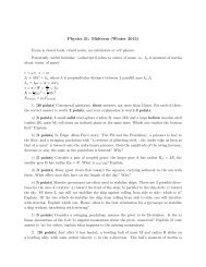
PDF (double-sided) - Physics Department, UCSB - University of ...
PDF (double-sided) - Physics Department, UCSB - University of ...
PDF (double-sided) - Physics Department, UCSB - University of ...

You also want an ePaper? Increase the reach of your titles
YUMPU automatically turns print PDFs into web optimized ePapers that Google loves.
UNIVERSITY <strong>of</strong> CALIFORNIA<br />
Santa Barbara<br />
Benchmarking the<br />
Superconducting Josephson Phase Qubit:<br />
The Violation <strong>of</strong> Bell’s Inequality<br />
A dissertation submitted in partial satisfaction <strong>of</strong> the<br />
requirements for the degree <strong>of</strong><br />
Doctor <strong>of</strong> Philosophy<br />
in<br />
<strong>Physics</strong><br />
by<br />
Markus Ansmann<br />
Committee in charge:<br />
Pr<strong>of</strong>essor John M. Martinis, Chair<br />
Pr<strong>of</strong>essor Andrew N. Cleland<br />
Pr<strong>of</strong>essor Andreas Ludwig<br />
June 2009
The dissertation <strong>of</strong> Markus Ansmann is approved:<br />
Pr<strong>of</strong>essor Andrew N. Cleland<br />
Pr<strong>of</strong>essor Andreas Ludwig<br />
Pr<strong>of</strong>essor John M. Martinis, Chair<br />
June 2009
Benchmarking the<br />
Superconducting Josephson Phase Qubit:<br />
The Violation <strong>of</strong> Bell’s Inequality<br />
Copyright 2009<br />
by<br />
Markus Ansmann<br />
v
To my parents,<br />
Klaus and Ulrike Ansmann,<br />
who made it possible for me to study abroad<br />
and who raised me to be persistent and crazy enough<br />
to complete the journey that led to this degree.<br />
vii
viii
Acknowledgements<br />
This work would not have been possible without the intellectual and emotional<br />
support <strong>of</strong> the many amazing people that I had the honor <strong>of</strong> sharing the past<br />
several years <strong>of</strong> my life with.<br />
First, I would like to thank my fiancée, Doctor Ekaterina Chernobai, for her<br />
never-ending patience and support during these crazy years. Ready for more?<br />
I thank Pr<strong>of</strong>essor John Martinis for the opportunity to be a member <strong>of</strong> his<br />
group and for being my research advisor. Working for John and having the chance<br />
to set up a new lab with him has been immensely helpful for me to grow as<br />
a scientist, a team-player, and a person. I owe a lot <strong>of</strong> insights about project<br />
management, leadership, and, <strong>of</strong> course, physics to our interactions.<br />
I am very grateful to Assistant Pr<strong>of</strong>essor Robert McDermott, Doctor Matthias<br />
Steffen, and Doctor Ken Cooper for helping me with my start into the field <strong>of</strong><br />
experimental condensed matter physics. Their coaching gave me the solid foundation<br />
on which I was able to build my thesis work while their great sense <strong>of</strong> humor<br />
helped me survive the beating with a smile.<br />
Without Doctor Haohua Wang this experiment would not have been possible<br />
since his incredible skill and dedication in the cleanroom resulted in the qubit<br />
devices that were the key to demonstrating the violation <strong>of</strong> the Bell inequality.<br />
I would like to specifically acknowledge Matthew Neeley, whose enthusiasm<br />
and support for LabRAD were instrumental in getting it to the level <strong>of</strong> quality<br />
at which it runs today. Matthew opened my eyes to the world <strong>of</strong> programming<br />
beyond Delphi and helped me significantly improve and diversify my skills.<br />
Erik Lucero played an important role in this work as well by always being<br />
ready to fix another blown fuse on the control electronics. His positive attitude<br />
and his love for Chai helped me keep my sanity and stay in touch with reality.<br />
I also thank Radek Bialczak, Aaron O’Connell, Doctor Max H<strong>of</strong>heinz, Daniel<br />
Sank, Jim Wenner, and Doctor Martin Weides. Their dedication to the team and<br />
sense <strong>of</strong> humor helped create a fun, yet extremely productive work environment.<br />
I would like to express my appreciation to the staff <strong>of</strong> the <strong>UCSB</strong> <strong>Physics</strong><br />
<strong>Department</strong>, the California NanoSystems Institute, the <strong>UCSB</strong> Machine Shop, and<br />
the <strong>UCSB</strong> Cleanroom. The infrastructure they provided was extremely helpful in<br />
efficiently meeting the challenges posed by the different steps <strong>of</strong> the project.<br />
I also thank Pr<strong>of</strong>essor Andrew Cleland and Pr<strong>of</strong>essor Andreas Ludwig for<br />
agreeing to be on my thesis committee and for putting up with my last-minute<br />
delivery <strong>of</strong> this work. Please accept my apologies.<br />
Finally, I would like to express my appreciation to my family and friends<br />
without whom I would have surely lost my mind over the course <strong>of</strong> the last years.<br />
ix
Curriculum Vitæ<br />
Markus Ansmann<br />
Education<br />
2009 Doctor <strong>of</strong> Philosophy, <strong>Physics</strong>, <strong>University</strong> <strong>of</strong> California, Santa Barbara<br />
(expected)<br />
2007 Master <strong>of</strong> Arts, Economics, <strong>University</strong> <strong>of</strong> California, Santa Barbara<br />
2007 Certificate, Graduate Program in Management Practice, <strong>University</strong><br />
<strong>of</strong> California, Santa Barbara<br />
2003 Bachelor <strong>of</strong> Science, <strong>Physics</strong>, <strong>University</strong> <strong>of</strong> California, Santa Barbara<br />
Publications<br />
Ansmann, M., Wang, H., Bialczak, R. C., H<strong>of</strong>heinz, M., Lucero, E., Neeley, M.,<br />
O’Connell, A. D., Sank, D., Weides, M., Wenner, J., Cleland, A. N., Martinis,<br />
J. M., “Violation <strong>of</strong> Bell’s inequality in Josephson phase qubits”, Submitted to<br />
Nature (2009)<br />
Martinis, J. M., Ansmann, M., and Aumentado, J., “Energy Decay in Josephson<br />
Qubits from Non-equilibrium Quasiparticles”, Submitted to Physical Review Letters<br />
(2009)<br />
H<strong>of</strong>heinz, M., Wang, H., Ansmann, M., Bialczak, R. C., Lucero, E., Neeley, M.,<br />
O’Connell, A. D., Sank, D., Wenner, J., Martinis, J. M., and Cleland, A. N.,<br />
“Synthesizing arbitrary quantum states in a superconducting resonator”, Nature<br />
(2009), 459:546-549<br />
Wang, H., H<strong>of</strong>heinz, M., Ansmann, M., Bialczak, R. C., Lucero, E., Neeley, M.,<br />
O’Connell, A. D., Sank, D., Wenner, J., Cleland, A. N., and Martinis, J. M.,<br />
“Measurement <strong>of</strong> the decay <strong>of</strong> Fock states in a superconducting quantum circuit”,<br />
Physical Review Letters (2008), 101:240401<br />
xi
Katz, N., Neeley, M., Ansmann, M., Bialczak, R. C., H<strong>of</strong>heinz, M., Lucero, E.,<br />
O’Connell, A. D., Wang, H., Cleland, A. N., Martinis, J. M., and Korotkov, A. N.,<br />
“Reversal <strong>of</strong> the Weak Measurement <strong>of</strong> a Quantum State in a Superconducting<br />
Phase Qubit”, Physical Review Letters (2008), 101:200401<br />
Levy, A. R., Leonardi, R., Ansmann, M., Bersanelli, M., Childers, J., Cole, T. D.,<br />
D’Arcangelo, O., Davis, G. V., Lubin, P. M., Marvil, J., Meinhold, P. R., Miller,<br />
G., O’Neill, H., Stavola, F., Stebor, N. C., Timbie, P. T., Van der Heide, M.,<br />
Villa, F., Villela, T., Williams, B. D., Wuensche, C. A., “The White Mountain<br />
Polarimeter Telescope and an Upper Limit on Cosmic Microwave Background Polarization”,<br />
Astrophysical Journal Supplement Series (2008), 177:419-430<br />
H<strong>of</strong>heinz, M., Weig, E. M., Ansmann, M., Bialczak, R. C., Lucero, E., Neeley, M.,<br />
O’Connell, A. D., Wang, H., Martinis J. M., and Cleland, A. N., “Generation <strong>of</strong><br />
Fock states in a superconducting quantum circuit”, Nature (2008), 454:310-314<br />
Neeley, M., Ansmann, M., Bialczak, R. C., H<strong>of</strong>heinz, M., Katz, N., Lucero, E.,<br />
O’Connell, A. D., Wang, H., Cleland, A. N., and Martinis J. M., “Process tomography<br />
<strong>of</strong> quantum memory in a Josephson-phase qubit coupled to a two-level<br />
state”, Nature <strong>Physics</strong> (2008), 4:523-526<br />
Lucero, E., H<strong>of</strong>heinz, M., Ansmann, M., Bialczak, R. C., Katz, N., Neeley, M.,<br />
OConnell, A.D., Wang, H., Cleland, A. N., and Martinis, J. M., “High-fidelity<br />
gates in a Josephson qubit”, Physical Review Letters (2008), 100:247001<br />
Neeley, M., Ansmann, M., Bialczak, R. C., H<strong>of</strong>heinz, M., Katz, N., Lucero, E.,<br />
OConnell, A. D., Wang, H., Cleland, A. N., and Martinis, J. M., “Transformed<br />
Dissipation in Superconducting Quantum Circuits”, Physical Review B (2008),<br />
77:180508<br />
O’Connell, A. D., Ansmann, M., Bialczak, R. C., H<strong>of</strong>heinz, M., Katz, N., Lucero,<br />
E., McKenney, C., Neeley, M., Wang, H., Weig, E. M., Cleland, A. N., and Martinis,<br />
J. M., “Microwave Dielectric Loss at Single Photon Energies and milliKelvin<br />
Temperatures”, Applied <strong>Physics</strong> Letters (2008), 92:112903<br />
Bialczak, R. C., McDermott, R., Ansmann, M., H<strong>of</strong>heinz, M., Katz, N., Lucero,<br />
E., Neeley, M., O’Connell, A. D., Wang, H., Cleland, A. N., and Martinis, J.<br />
M., “1/f Flux Noise in Josephson Phase Qubits”, Physical Review Letters (2007),<br />
xii
99:187006<br />
Lisenfeld, J., Lukashenko, A., Ansmann, M., Martinis, J. M., Ustinov, A. V.,<br />
“Temperature dependence <strong>of</strong> coherent oscillations in Josephson phase qubits”,<br />
Physical Review Letters (2007), 99:170504<br />
Steffen, M., Ansmann, M., Bialczak, R. C., Katz, N., Lucero, E., McDermott, R.,<br />
Neeley, M., Weig, E. M., Cleland, A. N., and Martinis, J. M., “Measurement <strong>of</strong><br />
the Entanglement <strong>of</strong> Two Superconducting Qubits via State Tomography”, Science<br />
(2006), 313:1423-1425<br />
Steffen, M., Ansmann, M., McDermott, R., Katz, N., Bialczak, R. C., Lucero, E.,<br />
Neeley, M., Weig, E. M., Cleland, A. N., and Martinis, J. M., “State tomography<br />
<strong>of</strong> capacitively shunted phase qubits with high fidelity”, Physical Review Letters<br />
(2006), 97:050502<br />
Katz, N., Ansmann, M., Bialczak, R. C., Lucero, E., McDermott, R., Neeley, M.,<br />
Steffen, M., Weig, E. M., Cleland, A. N., Martinis, J. M., and Korotkov, A. N.,<br />
“Coherent state evolution in a superconducting qubit from partial-collapse measurement”,<br />
Science (2006), 312: 1498-1500<br />
Marvil, J., Ansmann, M., Childers, J., Cole, T., Davis, G. V., Hadjiyska, E.,<br />
Halevi, D., Heimberg, G., Kangas, M., Levy, A., Leonardi, R., Lubin, P., Meinhold,<br />
P., O’Neill, H., Parendo, S., Quetin, E., Stebor, N., Villela, T., Williams, B.,<br />
Wuensche, C. A., and Yamaguchi, K., “An Astronomical Site Survey at the Barcr<strong>of</strong>t<br />
Facility <strong>of</strong> the White Mountain Research Station”, New Astronomy (2006),<br />
11:218-225<br />
Martinis, J. M., Cooper, K. B., McDermott, R., Steffen, M., Ansmann, M., Osborn,<br />
K., Cicak, K., Oh, S., Pappas, D. P., Simmonds, R.W., and Yu, C. C.,<br />
“Decoherence in Josephson Qubits from Dielectric Loss”, Physical Review Letters<br />
(2005), 95:210503<br />
Kangas, M. M., Ansmann, M., Copsey, K., Horgan, B., Leonardi, R., Lubin, P.,<br />
Villela, T., “A 100-GHz high-gain tilted corrugated nonbonded platelet antenna”,<br />
IEEE Antennas and Wireless Propagation Letters (2005), 4:304-307<br />
Kangas, M. M., Ansmann, M., Horgan, B., Lemaster, N., Leonardi, R., Levy,<br />
xiii
A., Lubin, P., Marvil, J., McCreary, P., Villela, T., “A 31 pixel flared 100-GHz<br />
high-gain scalar corrugated nonbonded platelet antenna array”, IEEE Antennas<br />
and Wireless Propagation Letters (2005), 4:245-248<br />
Honors and Awards<br />
2003 Arnold Nordsieck Award, <strong>Physics</strong> <strong>Department</strong>, <strong>University</strong> <strong>of</strong> California,<br />
Santa Barbara, California<br />
2003 Research Honors, <strong>Physics</strong> <strong>Department</strong>, <strong>University</strong> <strong>of</strong> California,<br />
Santa Barbara, California<br />
2003 Dean’s Honors, <strong>University</strong> <strong>of</strong> California, Santa Barbara, California<br />
1999 - 2001 Dean’s List, Stevens Institute <strong>of</strong> Technology, Hoboken, NJ<br />
xiv
Abstract<br />
Benchmarking the<br />
Superconducting Josephson Phase Qubit:<br />
The Violation <strong>of</strong> Bell’s Inequality<br />
by<br />
Markus Ansmann<br />
The concepts <strong>of</strong> entanglement and superpositions introduced by quantum mechanics<br />
promise to allow for the design <strong>of</strong> a new computing architecture, called<br />
a quantum computer, that can exponentially outperform any possible classical<br />
computer. Such a performance improvement would make presently intractable<br />
computational problems efficiently solvable. Such problems include optimizations,<br />
like the traveling salesman problem, factorization, and quantum simulations, e.g.<br />
for medical research.<br />
This thesis discusses one approach to implementing a quantum computer that<br />
is based on Superconducting Josephson Phase Qubits. An experiment is presented<br />
that shows a violation <strong>of</strong> Bell’s inequality using these qubits (quantum bits), i.e.<br />
it demonstrates that a pair <strong>of</strong> these qubits can be placed into a state that shows<br />
xv
a stronger correlation than possible for a classical pair <strong>of</strong> bits. This experiment<br />
meets a major mile-stone for the field <strong>of</strong> superconducting qubits as it provides<br />
strong evidence that the architecture will indeed be able to outperform classical<br />
systems.<br />
Furthermore, this experiment is the first demonstration <strong>of</strong> a violation <strong>of</strong> Bell’s<br />
inequality in a solid state system, and the first demonstration in a macroscopic<br />
quantum system. It therefore adds valuable supporting evidence that the new<br />
ideas proposed by quantum mechanics are indeed valid across different quantum<br />
systems and cannot be explained by a deterministic alternative theory.<br />
xvi
Contents<br />
Contents<br />
List <strong>of</strong> Figures<br />
List <strong>of</strong> Tables<br />
xvii<br />
xxv<br />
xxvii<br />
1 Quantum Computation 1<br />
1.1 Motivation . . . . . . . . . . . . . . . . . . . . . . . . . . . . . . . 1<br />
1.1.1 The Information Society . . . . . . . . . . . . . . . . . . . 1<br />
1.1.2 Moore’s Law . . . . . . . . . . . . . . . . . . . . . . . . . . 2<br />
1.1.3 Church-Turing Thesis . . . . . . . . . . . . . . . . . . . . . 2<br />
1.1.4 Deutsch-Josza Algorithm . . . . . . . . . . . . . . . . . . . 3<br />
1.1.5 Shor’s Algorithm . . . . . . . . . . . . . . . . . . . . . . . 4<br />
1.1.6 Quantum Annealing . . . . . . . . . . . . . . . . . . . . . 5<br />
1.1.7 Quantum Simulation . . . . . . . . . . . . . . . . . . . . . 5<br />
1.2 The Power <strong>of</strong> Quantum Computers . . . . . . . . . . . . . . . . . 6<br />
1.2.1 Superpositions . . . . . . . . . . . . . . . . . . . . . . . . . 6<br />
1.2.2 Entanglement . . . . . . . . . . . . . . . . . . . . . . . . . 7<br />
1.2.3 Implications – The EPR Paradox . . . . . . . . . . . . . . 9<br />
1.3 Requirements – The DiVincenzo Criteria . . . . . . . . . . . . . . 11<br />
1.3.1 Scalable Physical System with Well-Defined Qubits . . . . 12<br />
1.3.2 Initializable to a Simple Fiducial State . . . . . . . . . . . 12<br />
1.3.3 Sufficiently Long Coherence Times . . . . . . . . . . . . . 12<br />
1.3.4 Universal Set <strong>of</strong> Quantum Gates . . . . . . . . . . . . . . . 13<br />
1.3.5 High Quantum Efficiency, Qubit-Specific Measurements . . 14<br />
xvii
2 Superconducting Josephson Qubits 15<br />
2.1 Motivation . . . . . . . . . . . . . . . . . . . . . . . . . . . . . . . 15<br />
2.1.1 Long Coherence Time . . . . . . . . . . . . . . . . . . . . 16<br />
2.1.2 Scalability . . . . . . . . . . . . . . . . . . . . . . . . . . . 16<br />
2.1.3 Initialization, Control and Measurement . . . . . . . . . . 17<br />
2.2 Idea . . . . . . . . . . . . . . . . . . . . . . . . . . . . . . . . . . 18<br />
2.2.1 Quantum Mechanics in Electrical Circuits . . . . . . . . . 18<br />
2.2.2 Josephson Tunnel Junctions . . . . . . . . . . . . . . . . . 22<br />
2.2.3 Circuit Potential . . . . . . . . . . . . . . . . . . . . . . . 25<br />
2.2.4 Circuit Parameters . . . . . . . . . . . . . . . . . . . . . . 27<br />
2.3 Superconducting Qubit Operation . . . . . . . . . . . . . . . . . . 29<br />
2.3.1 Initialization . . . . . . . . . . . . . . . . . . . . . . . . . . 29<br />
2.3.2 Single Qubit Gates . . . . . . . . . . . . . . . . . . . . . . 30<br />
2.3.3 Multi Qubit Coupling . . . . . . . . . . . . . . . . . . . . 31<br />
2.3.4 Readout . . . . . . . . . . . . . . . . . . . . . . . . . . . . 32<br />
3 Understanding Qubits Numerically 37<br />
3.1 Solving the Schrödinger Equation . . . . . . . . . . . . . . . . . . 37<br />
3.1.1 Time Dependent versus Time Independent Part . . . . . . 38<br />
3.1.2 Effects <strong>of</strong> a Time Dependent Potential . . . . . . . . . . . 40<br />
3.2 Finding Eigenstates Numerically . . . . . . . . . . . . . . . . . . . 41<br />
3.2.1 The Eigenstates <strong>of</strong> the Qubit Potential . . . . . . . . . . . 45<br />
3.2.2 Eigenstates <strong>of</strong> Coupled Qubit Systems . . . . . . . . . . . 47<br />
3.3 Interaction with the Qubit . . . . . . . . . . . . . . . . . . . . . . 49<br />
3.3.1 Interactions as Rotations on the Bloch Sphere . . . . . . . 54<br />
3.3.2 Operations on a Single Qubit . . . . . . . . . . . . . . . . 57<br />
3.3.3 Single Qubit Operations in a Coupled System . . . . . . . 59<br />
3.3.4 Qubit Coupling . . . . . . . . . . . . . . . . . . . . . . . . 60<br />
3.4 Simulating Imperfections . . . . . . . . . . . . . . . . . . . . . . . 61<br />
3.4.1 Measurement Fidelities . . . . . . . . . . . . . . . . . . . . 61<br />
3.4.2 Measurement Crosstalk . . . . . . . . . . . . . . . . . . . . 62<br />
3.4.3 Microwave Crosstalk . . . . . . . . . . . . . . . . . . . . . 63<br />
3.4.4 Decoherence – The Density Matrix Formalism . . . . . . . 63<br />
3.4.5 Decoherence – The Kraus Operators . . . . . . . . . . . . 66<br />
4 Designing the Phase Qubit Integrated Circuit 69<br />
4.1 Electrical Circuit Design . . . . . . . . . . . . . . . . . . . . . . . 70<br />
4.1.1 Qubit Circuit Parameters . . . . . . . . . . . . . . . . . . 71<br />
4.1.2 Biasing Circuit Parameters . . . . . . . . . . . . . . . . . . 73<br />
xviii
4.1.3 Readout Squid Parameters . . . . . . . . . . . . . . . . . . 75<br />
4.1.4 Coupler Circuit . . . . . . . . . . . . . . . . . . . . . . . . 79<br />
4.2 Geometric Circuit Element Layout . . . . . . . . . . . . . . . . . 81<br />
4.2.1 Qubit . . . . . . . . . . . . . . . . . . . . . . . . . . . . . 82<br />
4.2.2 Bias Coil . . . . . . . . . . . . . . . . . . . . . . . . . . . . 84<br />
4.2.3 Squid . . . . . . . . . . . . . . . . . . . . . . . . . . . . . 84<br />
4.3 Materials and Processes . . . . . . . . . . . . . . . . . . . . . . . 85<br />
4.3.1 Superconductor . . . . . . . . . . . . . . . . . . . . . . . . 85<br />
4.3.2 Junction Dielectrics . . . . . . . . . . . . . . . . . . . . . . 85<br />
4.3.3 Crossover Dielectric . . . . . . . . . . . . . . . . . . . . . . 86<br />
4.3.4 Wafer . . . . . . . . . . . . . . . . . . . . . . . . . . . . . 87<br />
5 Phase Qubit Fabrication 89<br />
5.1 Mask Design . . . . . . . . . . . . . . . . . . . . . . . . . . . . . . 89<br />
5.2 Fabrication Overview . . . . . . . . . . . . . . . . . . . . . . . . . 91<br />
5.3 Base Wiring Layer . . . . . . . . . . . . . . . . . . . . . . . . . . 92<br />
5.3.1 Aluminum Sputter Deposition . . . . . . . . . . . . . . . . 92<br />
5.3.2 Lithography . . . . . . . . . . . . . . . . . . . . . . . . . . 93<br />
5.3.3 ICP Etch . . . . . . . . . . . . . . . . . . . . . . . . . . . 95<br />
5.3.4 Photo-Resist Strip . . . . . . . . . . . . . . . . . . . . . . 95<br />
5.4 Insulator Layer – Part I . . . . . . . . . . . . . . . . . . . . . . . 96<br />
5.4.1 PECVD Deposition . . . . . . . . . . . . . . . . . . . . . . 96<br />
5.4.2 Via Cut . . . . . . . . . . . . . . . . . . . . . . . . . . . . 97<br />
5.5 Top Wiring Layer – Part I . . . . . . . . . . . . . . . . . . . . . . 98<br />
5.5.1 Argon Mill . . . . . . . . . . . . . . . . . . . . . . . . . . . 98<br />
5.5.2 Aluminum Deposition . . . . . . . . . . . . . . . . . . . . 99<br />
5.5.3 Junction Gap Cut . . . . . . . . . . . . . . . . . . . . . . . 99<br />
5.6 Junction Layers . . . . . . . . . . . . . . . . . . . . . . . . . . . . 100<br />
5.6.1 Oxidation / Deposition . . . . . . . . . . . . . . . . . . . . 100<br />
5.6.2 Junction Definition via Argon-Chlorine Etch . . . . . . . . 100<br />
5.7 Top Wiring Layer – Part II . . . . . . . . . . . . . . . . . . . . . 102<br />
5.8 Insulator Layer – Part II . . . . . . . . . . . . . . . . . . . . . . . 102<br />
5.9 Top Wiring Layer – Part III . . . . . . . . . . . . . . . . . . . . . 103<br />
5.10 Dicing . . . . . . . . . . . . . . . . . . . . . . . . . . . . . . . . . 103<br />
6 Device Testing Equipment 105<br />
6.1 Physical Quality Control during Fabrication . . . . . . . . . . . . 106<br />
6.1.1 Optical Microscopy . . . . . . . . . . . . . . . . . . . . . . 106<br />
6.1.2 Scanning Electron Microscopy . . . . . . . . . . . . . . . . 107<br />
xix
6.1.3 Atomic Force Microscopy . . . . . . . . . . . . . . . . . . . 108<br />
6.1.4 Dektak . . . . . . . . . . . . . . . . . . . . . . . . . . . . . 108<br />
6.2 Electrical Screening after Fabrication . . . . . . . . . . . . . . . . 109<br />
6.2.1 4-Wire Measurements . . . . . . . . . . . . . . . . . . . . . 109<br />
6.2.2 Adiabatic Demagnetization Refrigerator . . . . . . . . . . 110<br />
6.3 Quantum Measurements at 25 mK . . . . . . . . . . . . . . . . . . 112<br />
6.3.1 Dilution Refrigerator . . . . . . . . . . . . . . . . . . . . . 112<br />
6.3.2 Sample Mount . . . . . . . . . . . . . . . . . . . . . . . . . 113<br />
6.3.3 Wire Bonding . . . . . . . . . . . . . . . . . . . . . . . . . 114<br />
6.3.4 Dilution Refrigerator Wiring . . . . . . . . . . . . . . . . . 115<br />
6.3.5 FastBias Card . . . . . . . . . . . . . . . . . . . . . . . . . 117<br />
6.3.6 PreAmp Card . . . . . . . . . . . . . . . . . . . . . . . . . 118<br />
6.3.7 Bias Box . . . . . . . . . . . . . . . . . . . . . . . . . . . . 118<br />
6.3.8 GHz DACs . . . . . . . . . . . . . . . . . . . . . . . . . . 119<br />
6.3.9 Anritsu Microwave Source . . . . . . . . . . . . . . . . . . 120<br />
6.3.10 Microwave Components . . . . . . . . . . . . . . . . . . . 120<br />
7 Control S<strong>of</strong>tware – LabRAD 123<br />
7.1 Motivation . . . . . . . . . . . . . . . . . . . . . . . . . . . . . . . 123<br />
7.2 Requirements . . . . . . . . . . . . . . . . . . . . . . . . . . . . . 124<br />
7.2.1 Scalability . . . . . . . . . . . . . . . . . . . . . . . . . . . 124<br />
7.2.2 Maintainability . . . . . . . . . . . . . . . . . . . . . . . . 125<br />
7.2.3 Efficiency . . . . . . . . . . . . . . . . . . . . . . . . . . . 127<br />
7.2.4 Performance . . . . . . . . . . . . . . . . . . . . . . . . . . 128<br />
7.3 Approach . . . . . . . . . . . . . . . . . . . . . . . . . . . . . . . 128<br />
7.3.1 Modularity . . . . . . . . . . . . . . . . . . . . . . . . . . 128<br />
7.3.2 Network Distribution . . . . . . . . . . . . . . . . . . . . . 133<br />
7.3.3 Cross-Language and Cross-Platform . . . . . . . . . . . . . 135<br />
7.3.4 Performance . . . . . . . . . . . . . . . . . . . . . . . . . . 136<br />
7.3.5 Open-Source . . . . . . . . . . . . . . . . . . . . . . . . . . 136<br />
7.4 Components . . . . . . . . . . . . . . . . . . . . . . . . . . . . . . 137<br />
7.4.1 LabRAD Protocol . . . . . . . . . . . . . . . . . . . . . . . 137<br />
7.4.2 LabRAD Manager . . . . . . . . . . . . . . . . . . . . . . 143<br />
7.4.3 LabRAD APIs . . . . . . . . . . . . . . . . . . . . . . . . 146<br />
7.5 Our Setup . . . . . . . . . . . . . . . . . . . . . . . . . . . . . . . 152<br />
7.5.1 Overview . . . . . . . . . . . . . . . . . . . . . . . . . . . 152<br />
7.5.2 DC Rack Controller . . . . . . . . . . . . . . . . . . . . . . 155<br />
7.5.3 DC Rack Server . . . . . . . . . . . . . . . . . . . . . . . . 156<br />
7.5.4 Serial Server . . . . . . . . . . . . . . . . . . . . . . . . . . 156<br />
xx
7.5.5 Grapher . . . . . . . . . . . . . . . . . . . . . . . . . . . . 157<br />
7.5.6 Data Vault . . . . . . . . . . . . . . . . . . . . . . . . . . 158<br />
7.5.7 Registry Editor / Server . . . . . . . . . . . . . . . . . . . 159<br />
7.5.8 Sweep Client / Server . . . . . . . . . . . . . . . . . . . . . 160<br />
7.5.9 Optimizer Client / Server . . . . . . . . . . . . . . . . . . 162<br />
7.5.10 Experiment Servers . . . . . . . . . . . . . . . . . . . . . . 162<br />
7.5.11 Qubit Bias Server . . . . . . . . . . . . . . . . . . . . . . . 164<br />
7.5.12 Qubit Server . . . . . . . . . . . . . . . . . . . . . . . . . . 164<br />
7.5.13 DAC Calibration Server . . . . . . . . . . . . . . . . . . . 166<br />
7.5.14 GHz DAC Server . . . . . . . . . . . . . . . . . . . . . . . 167<br />
7.5.15 Direct Ethernet Server . . . . . . . . . . . . . . . . . . . . 168<br />
7.5.16 Anritsu, Sampling Scope, and Spectrum Analyzer Servers . 169<br />
7.5.17 GPIB Server . . . . . . . . . . . . . . . . . . . . . . . . . . 170<br />
7.5.18 IPython . . . . . . . . . . . . . . . . . . . . . . . . . . . . 171<br />
8 Single Qubit Bring-Up and Characterization 173<br />
8.1 Squid I/V Response . . . . . . . . . . . . . . . . . . . . . . . . . . 174<br />
8.2 Squid Steps . . . . . . . . . . . . . . . . . . . . . . . . . . . . . . 176<br />
8.3 Step Edge . . . . . . . . . . . . . . . . . . . . . . . . . . . . . . . 182<br />
8.4 RF bias . . . . . . . . . . . . . . . . . . . . . . . . . . . . . . . . 185<br />
8.5 S-Curve . . . . . . . . . . . . . . . . . . . . . . . . . . . . . . . . 187<br />
8.6 Spectroscopy . . . . . . . . . . . . . . . . . . . . . . . . . . . . . 189<br />
8.7 Rabi Oscillation . . . . . . . . . . . . . . . . . . . . . . . . . . . . 189<br />
8.8 Visibility . . . . . . . . . . . . . . . . . . . . . . . . . . . . . . . . 193<br />
8.9 T 1 . . . . . . . . . . . . . . . . . . . . . . . . . . . . . . . . . . . 194<br />
8.10 Ramsey . . . . . . . . . . . . . . . . . . . . . . . . . . . . . . . . 195<br />
8.11 Spin-Echo . . . . . . . . . . . . . . . . . . . . . . . . . . . . . . . 197<br />
8.12 2D-Spectroscopy . . . . . . . . . . . . . . . . . . . . . . . . . . . 199<br />
9 Coupled Qubit Bringup 201<br />
9.1 Controlling Multiple Qubits . . . . . . . . . . . . . . . . . . . . . 201<br />
9.1.1 Control Synchronization . . . . . . . . . . . . . . . . . . . 201<br />
9.1.2 Flux Bias Crosstalk . . . . . . . . . . . . . . . . . . . . . . 203<br />
9.1.3 Readout Squid Crosstalk . . . . . . . . . . . . . . . . . . . 204<br />
9.2 Always-On Capacitive Coupling . . . . . . . . . . . . . . . . . . . 206<br />
9.2.1 Measurement Crosstalk and Timing . . . . . . . . . . . . . 206<br />
9.2.2 Spectroscopy . . . . . . . . . . . . . . . . . . . . . . . . . 208<br />
9.2.3 Swaps . . . . . . . . . . . . . . . . . . . . . . . . . . . . . 209<br />
9.2.4 Resonance Calibration . . . . . . . . . . . . . . . . . . . . 211<br />
xxi
9.2.5 Phase Calibration . . . . . . . . . . . . . . . . . . . . . . . 213<br />
9.2.6 “Controllable Coupling” via Bias Changes . . . . . . . . . 214<br />
9.3 Resonator Based Coupling . . . . . . . . . . . . . . . . . . . . . . 215<br />
9.3.1 2D-Spectroscopy . . . . . . . . . . . . . . . . . . . . . . . 217<br />
9.3.2 Swapping a Photon into the Resonator . . . . . . . . . . . 217<br />
9.3.3 Retrieving the Photon from the Resonator . . . . . . . . . 218<br />
9.3.4 Timing Calibration . . . . . . . . . . . . . . . . . . . . . . 220<br />
9.3.5 Swaps . . . . . . . . . . . . . . . . . . . . . . . . . . . . . 221<br />
9.3.6 Resonator T 1 and T 2 . . . . . . . . . . . . . . . . . . . . . 222<br />
10 Hidden Variable Theories versus Quantum Mechanics 225<br />
10.1 Introduction . . . . . . . . . . . . . . . . . . . . . . . . . . . . . . 225<br />
10.1.1 Is Quantum Mechanics Incomplete? . . . . . . . . . . . . . 225<br />
10.1.2 Is Quantum Mechanics Wrong? . . . . . . . . . . . . . . . 226<br />
10.1.3 Settling the Question Experimentally . . . . . . . . . . . . 226<br />
10.2 Experimental Results . . . . . . . . . . . . . . . . . . . . . . . . . 233<br />
10.2.1 Photons . . . . . . . . . . . . . . . . . . . . . . . . . . . . 233<br />
10.2.2 Ions . . . . . . . . . . . . . . . . . . . . . . . . . . . . . . 234<br />
10.2.3 Ion and Photon . . . . . . . . . . . . . . . . . . . . . . . . 235<br />
10.3 The Bell Inequality versus Phase Qubits? . . . . . . . . . . . . . . 236<br />
11 Implementing the Bell Test 239<br />
11.1 State Preparation . . . . . . . . . . . . . . . . . . . . . . . . . . . 240<br />
11.1.1 Initialization in the | 10 〉 state . . . . . . . . . . . . . . . . 240<br />
11.1.2 Entangling the Qubits – Capacitive Coupling . . . . . . . 240<br />
11.1.3 Entangling the Qubits – Resonator Coupling . . . . . . . . 241<br />
11.1.4 Verifying Entanglement – State Tomography . . . . . . . . 244<br />
11.2 Correlation Measurements . . . . . . . . . . . . . . . . . . . . . . 246<br />
11.2.1 Bell Rotations . . . . . . . . . . . . . . . . . . . . . . . . . 247<br />
11.2.2 Tunneling Measurement . . . . . . . . . . . . . . . . . . . 247<br />
11.2.3 Statistical Analysis . . . . . . . . . . . . . . . . . . . . . . 248<br />
11.3 Calibration . . . . . . . . . . . . . . . . . . . . . . . . . . . . . . 250<br />
11.3.1 Global Optimization . . . . . . . . . . . . . . . . . . . . . 250<br />
11.3.2 Manual Search . . . . . . . . . . . . . . . . . . . . . . . . 251<br />
11.3.3 Nelder-Mead Simplex Algorithm . . . . . . . . . . . . . . . 255<br />
11.3.4 Particle Swarm Optimization . . . . . . . . . . . . . . . . 256<br />
11.4 Experimental Results . . . . . . . . . . . . . . . . . . . . . . . . . 258<br />
11.4.1 Capacitive Coupling . . . . . . . . . . . . . . . . . . . . . 259<br />
11.4.2 Resonator Coupling . . . . . . . . . . . . . . . . . . . . . . 263<br />
xxii
11.5 Analysis and Verification . . . . . . . . . . . . . . . . . . . . . . . 267<br />
11.5.1 Standard Error <strong>of</strong> the S-Value . . . . . . . . . . . . . . . . 267<br />
11.5.2 Dependence <strong>of</strong> S on Sequence Parameters . . . . . . . . . 270<br />
11.5.3 Microwave and Measurement Crosstalk . . . . . . . . . . . 272<br />
11.5.4 Numerical Simulation . . . . . . . . . . . . . . . . . . . . . 275<br />
11.5.5 Measurement Correction . . . . . . . . . . . . . . . . . . . 280<br />
12 Conclusion 283<br />
12.1 Claim <strong>of</strong> Violation <strong>of</strong> Bell’s Inequality . . . . . . . . . . . . . . . . 283<br />
12.2 S-Value as Qubit Pair Benchmark . . . . . . . . . . . . . . . . . . 284<br />
12.3 Josephson Phase Qubit Performance . . . . . . . . . . . . . . . . 285<br />
12.4 Future Direction . . . . . . . . . . . . . . . . . . . . . . . . . . . 286<br />
xxiii
xxiv
List <strong>of</strong> Figures<br />
2.1 Inductor-Capacitor Oscillator . . . . . . . . . . . . . . . . . . . . 19<br />
2.2 Josephson Tunnel Junction . . . . . . . . . . . . . . . . . . . . . . 23<br />
2.3 Modified Inductor-Capacitor Oscillator . . . . . . . . . . . . . . . 26<br />
2.4 Josephson Qubits . . . . . . . . . . . . . . . . . . . . . . . . . . . 27<br />
2.5 Example Qubit Coupling Circuits . . . . . . . . . . . . . . . . . . 30<br />
2.6 Squid Readout Scheme . . . . . . . . . . . . . . . . . . . . . . . . 34<br />
3.1 Examples <strong>of</strong> Numerical Eigenstate Solutions . . . . . . . . . . . . 44<br />
3.2 Simulation <strong>of</strong> LC Oscillator . . . . . . . . . . . . . . . . . . . . . 50<br />
3.3 Simulation <strong>of</strong> Mock-Qubit . . . . . . . . . . . . . . . . . . . . . . 51<br />
3.4 Bloch Sphere . . . . . . . . . . . . . . . . . . . . . . . . . . . . . 55<br />
4.1 Qubit Circuit . . . . . . . . . . . . . . . . . . . . . . . . . . . . . 70<br />
4.2 Readout Squid . . . . . . . . . . . . . . . . . . . . . . . . . . . . 76<br />
4.3 Squid I/V Traces . . . . . . . . . . . . . . . . . . . . . . . . . . . 79<br />
4.4 Spice Coupler Design . . . . . . . . . . . . . . . . . . . . . . . . . 80<br />
4.5 Qubit Integrated Circuit . . . . . . . . . . . . . . . . . . . . . . . 81<br />
5.1 L-Edit Mask Layout Tool . . . . . . . . . . . . . . . . . . . . . . 90<br />
5.2 Fabrication Building Blocks . . . . . . . . . . . . . . . . . . . . . 92<br />
5.3 Photolithography and Etching . . . . . . . . . . . . . . . . . . . . 94<br />
5.4 Clearing Vias from Native Oxide . . . . . . . . . . . . . . . . . . 98<br />
5.5 3D View <strong>of</strong> Junction . . . . . . . . . . . . . . . . . . . . . . . . . 101<br />
6.1 4-Wire Measurement . . . . . . . . . . . . . . . . . . . . . . . . . 110<br />
6.2 Dilution Refrigerator Wiring . . . . . . . . . . . . . . . . . . . . . 116<br />
7.1 Control Layout . . . . . . . . . . . . . . . . . . . . . . . . . . . . 153<br />
xxv
8.1 Squid I/V . . . . . . . . . . . . . . . . . . . . . . . . . . . . . . . 175<br />
8.2 Squid Steps . . . . . . . . . . . . . . . . . . . . . . . . . . . . . . 177<br />
8.3 Squid Steps Failure Modes . . . . . . . . . . . . . . . . . . . . . . 180<br />
8.4 Step Edge . . . . . . . . . . . . . . . . . . . . . . . . . . . . . . . 183<br />
8.5 General Bias Sequence . . . . . . . . . . . . . . . . . . . . . . . . 186<br />
8.6 Step Edge . . . . . . . . . . . . . . . . . . . . . . . . . . . . . . . 187<br />
8.7 Spectroscopy . . . . . . . . . . . . . . . . . . . . . . . . . . . . . 188<br />
8.8 Rabi Oscillation . . . . . . . . . . . . . . . . . . . . . . . . . . . . 190<br />
8.9 Visibility . . . . . . . . . . . . . . . . . . . . . . . . . . . . . . . . 193<br />
8.10 T 1 . . . . . . . . . . . . . . . . . . . . . . . . . . . . . . . . . . . 194<br />
8.11 Ramsey . . . . . . . . . . . . . . . . . . . . . . . . . . . . . . . . 196<br />
8.12 Spin Echo . . . . . . . . . . . . . . . . . . . . . . . . . . . . . . . 197<br />
8.13 Fine Spectroscopy . . . . . . . . . . . . . . . . . . . . . . . . . . . 199<br />
9.1 Effect <strong>of</strong> Squid Crosstalk on Step Edge . . . . . . . . . . . . . . . 205<br />
9.2 Measure Pulse Timing . . . . . . . . . . . . . . . . . . . . . . . . 207<br />
9.3 Spectroscopy <strong>of</strong> Coupled Qubits . . . . . . . . . . . . . . . . . . . 209<br />
9.4 Capacitive Coupling Swaps . . . . . . . . . . . . . . . . . . . . . . 210<br />
9.5 Capacitive Coupling Resonance Calibration . . . . . . . . . . . . 211<br />
9.6 Capacitive Coupling Phase Calibration . . . . . . . . . . . . . . . 212<br />
9.7 Fine Spectroscopy <strong>of</strong> Resonator Coupling . . . . . . . . . . . . . . 216<br />
9.8 Swapping Photon into Resonator . . . . . . . . . . . . . . . . . . 218<br />
9.9 Swapping Photon out <strong>of</strong> Resonator . . . . . . . . . . . . . . . . . 219<br />
9.10 Resonator Swaps . . . . . . . . . . . . . . . . . . . . . . . . . . . 221<br />
9.11 Resonator T 1 . . . . . . . . . . . . . . . . . . . . . . . . . . . . . 222<br />
11.1 Bell State Preparation . . . . . . . . . . . . . . . . . . . . . . . . 242<br />
11.2 Bell Measurements . . . . . . . . . . . . . . . . . . . . . . . . . . 246<br />
11.3 Standard Error Analysis . . . . . . . . . . . . . . . . . . . . . . . 266<br />
11.4 Behavior <strong>of</strong> S . . . . . . . . . . . . . . . . . . . . . . . . . . . . . 271<br />
11.5 Quantifying Measurement Crosstalk . . . . . . . . . . . . . . . . . 273<br />
11.6 Resonator Coupled Sample Specifications . . . . . . . . . . . . . . 276<br />
11.7 Visibility Analysis – Resonator Coupled Sample . . . . . . . . . . 279<br />
xxvi
List <strong>of</strong> Tables<br />
3.1 Transition Matrix Elements for Qubit-Like Potential . . . . . . . 52<br />
7.1 Basic LabRAD Types . . . . . . . . . . . . . . . . . . . . . . . . . 139<br />
7.2 Composite LabRAD Types . . . . . . . . . . . . . . . . . . . . . . 139<br />
7.3 LabRAD Type Annotations . . . . . . . . . . . . . . . . . . . . . 140<br />
7.4 LabRAD Data Flattening Rules . . . . . . . . . . . . . . . . . . . 140<br />
7.5 LabRAD Packet Structure ((ww)iws) . . . . . . . . . . . . . . . . 141<br />
7.6 LabRAD Record Structure (wss) . . . . . . . . . . . . . . . . . . 141<br />
10.1 Possible Populations for Locally Deterministic Particle Pairs . . . 228<br />
11.1 Entangled State Density Matrix – Raw . . . . . . . . . . . . . . . 244<br />
11.2 Entangled State Density Matrix – Corrected for Visibilities . . . . 244<br />
11.3 Sequence Parameters – Capacitive State Preparation . . . . . . . 251<br />
11.4 Sequence Parameters – Resonator State Preparation . . . . . . . . 252<br />
11.5 Sequence Parameters – Correlation Measurement . . . . . . . . . 253<br />
11.6 Qubit Sample Parameters – Capacitive Coupling Implementation 259<br />
11.7 Bell Violation Results – Capacitive Coupling Implementation . . . 260<br />
11.8 Optimization Results – Capacitive Coupling Implementation . . . 261<br />
11.9 Error Budget – Capacitive Coupling Implementation . . . . . . . 262<br />
11.10Bell Violation Results Total – Resonator Coupling . . . . . . . . . 264<br />
11.11Optimization Results – Resonator Coupling Implementation . . . 265<br />
11.12Bell Violation Results By Section – Resonator Coupling . . . . . . 268<br />
11.13Qubit Sample Parameters – Resonator Coupling Implementation . 277<br />
11.14Error Budget – Resonator Coupling Implementation . . . . . . . . 280<br />
11.15Bell Violation Results Corrected – Resonator Coupling . . . . . . 282<br />
xxvii
xxviii
Chapter 1<br />
Quantum Computation<br />
1.1 Motivation<br />
1.1.1 The Information Society<br />
During the 20 th century, information-intensive activities have grown from a<br />
few percent to two-thirds <strong>of</strong> all US labor [Molitor, 1982]. This was made possible<br />
by the advent <strong>of</strong> the personal computer and the increasingly wide-spread availability<br />
<strong>of</strong> information storage and sharing systems like magnetic hard disks and<br />
the Internet. The exponential improvements in performance and the drop in price<br />
<strong>of</strong> information gathering and creating devices has lead to an information deluge<br />
that is projected to result in a doubling <strong>of</strong> the world’s information base every 11<br />
1
hours by 2010 [Coles et al., 2006]. To handle this flood <strong>of</strong> information efficiently it<br />
will need to be met with a continuing dramatic increase in information processing<br />
power.<br />
1.1.2 Moore’s Law<br />
For the past 40 years, the performance <strong>of</strong> computing devices has <strong>double</strong>d<br />
roughly every 18 months. This trend is commonly referred to as “Moore’s Law”,<br />
inspired by an article written in 1965 by Intel co-founder Gordon Moore [Moore,<br />
1965]. Despite the fact that Moore’s Law is expected to hold for at least another<br />
decade, it is important to prepare for the longer term future when transistors on<br />
silicon will have been pushed to their limits.<br />
1.1.3 Church-Turing Thesis<br />
The Church-Turing Thesis makes this even more pressing. Alan Turing in 1938<br />
described a universal logic machine [Turing, 1938] that can efficiently, i.e. in polynomial<br />
time, simulate any other computing system. This logic machine is simple<br />
enough to allow any classical computer to simulate it efficiently as well. Therefore,<br />
any classical computer can simulate any other computing system efficiently. This<br />
implies that problems that are intractable, i.e. not solvable in polynomial time,<br />
on current computers will remain intractable on all future computers. Examples<br />
2
for such problems include factoring the product <strong>of</strong> two n-bit primes, the travelling<br />
salesman problem, the hidden subgroup problem, etc.<br />
1.1.4 Deutsch-Josza Algorithm<br />
In 1992, David Deutsch and Richard Jozsa proposed a fictitious problem and an<br />
algorithm for solving it that indicates that a computer which uses quantum states<br />
for computation might not be subject to this limitation imposed by the Church-<br />
Turing Thesis [Deutsch and Jozsa, 1992]. The problem consists <strong>of</strong> determining the<br />
nature <strong>of</strong> an unknown function by queries to an oracle that evaluates the function<br />
for a given input. The function acts on an n-bit number and is known to be either<br />
constant, i.e. returns 0 (or 1) for all possible inputs, or balanced, i.e. returns 0<br />
for exactly half <strong>of</strong> all possible inputs and 1 for all others. A classical computer,<br />
in the worst case, would have to evaluate the function 2 n−1 + 1 times, while a<br />
quantum computer would need to evaluate the function only once to determine<br />
with certainty whether it is balanced or constant. This is done by evaluating the<br />
function once for an input state that consists <strong>of</strong> a superposition <strong>of</strong> all possible 2 n<br />
states (achievable by the application <strong>of</strong> a Hadamard gate (see Section 1.3.4) to<br />
all input qubits). If the output shows amplitudes for both 0 and 1 the function is<br />
balanced, otherwise it is constant.<br />
This algorithm implies that a quantum computer might be infinitely faster than<br />
3
any possible classical computer for certain classes <strong>of</strong> problems that are considered<br />
intractable for classical computers.<br />
1.1.5 Shor’s Algorithm<br />
Perhaps the most practical example <strong>of</strong> this is the problem <strong>of</strong> factoring the<br />
product N <strong>of</strong> two large primes. The best currently known classical algorithm, the<br />
general number field sieve [Lenstra and Lenstra, 1993], requires sub-exponential<br />
time O(e (log N)1/3 (log log N) 2/3 ), while a quantum computing algorithm proposed by<br />
Peter Shor in 1997 requires polynomial time O((log N) 3 ) [Shor, 1997].<br />
The algorithm is based on reducing the factoring problem to the problem <strong>of</strong><br />
finding the period r <strong>of</strong> the function f(x) = a x mod N, where a is a random number<br />
less than N. If a and r fulfill certain requirements, one <strong>of</strong> the factors <strong>of</strong> N is the<br />
gcd(a r/2 ± 1, N), otherwise the procedure is repeated for a new random value for<br />
a. This approach makes use <strong>of</strong> the quantum computer’s power by employing it for<br />
the period finding step. Since the quantum computer can evaluate f(x) for many<br />
values <strong>of</strong> x simultaneously, it can very quickly generate the period r by fourier<br />
transforming interference patterns <strong>of</strong> different evaluations <strong>of</strong> f(x).<br />
Many <strong>of</strong> the modern data encryption schemes, e.g. RSA, are based on the<br />
intractability <strong>of</strong> the factoring problem. Therefore there is great interest by intelligence<br />
agencies to develop a system that can implement Shor’s algorithm to gauge<br />
4
if present encrypted data will remain secure in the future.<br />
1.1.6 Quantum Annealing<br />
Another problem <strong>of</strong> great interest is that <strong>of</strong> function optimization. The biggest<br />
challenge in optimization is finding global rather than local optima. A quantum<br />
computer is speculated to be very efficient at achieving this by allowing the “solution”<br />
to tunnel out <strong>of</strong> local minima that it might be stuck in [Apolloni et al.,<br />
1989]. A possible implementation would consist <strong>of</strong> encoding the function to be<br />
optimized into an energy potential landscape. For this, the quantum system is<br />
initially prepared in its state <strong>of</strong> lowest energy. If the potential <strong>of</strong> interest is turned<br />
on slowly enough, the system will adiabatically remain in its ground-state. After<br />
the potential is fully turned on, this ground-state will encode the solution to the<br />
optimization problem.<br />
1.1.7 Quantum Simulation<br />
In analogy to the Church-Turing Thesis, it has been shown that every physical<br />
quantum system can be simulated efficiently on a general quantum computer<br />
[Deutsch, 1985]. Such capabilities would be extremely helpful in fields like chemistry<br />
and medicine, where they would allow a more detailed understanding <strong>of</strong><br />
complex molecules and their interactions.<br />
5
1.2 The Power <strong>of</strong> Quantum Computers<br />
The power <strong>of</strong> quantum computers roots in two revolutionary concepts that<br />
quantum mechanics introduced: Superpositions and Entanglement.<br />
1.2.1 Superpositions<br />
According to quantum mechanics any system is described by a set <strong>of</strong> discrete<br />
states in which it can exist: the system’s “eigenstates”.<br />
It is possible for the<br />
system to exist in a superposition <strong>of</strong> these states, i.e. to be in multiple states<br />
at the same time. For example, a quantum bit can not only be in the 0 or 1<br />
state, but it can be in both, 0 and 1, at the same time. To describe the full<br />
state <strong>of</strong> a quantum system, each eigenstate is given a complex amplitude that<br />
describes its weight, called the “probability amplitude”. A measurement <strong>of</strong> the<br />
system will then force it to “choose” between one <strong>of</strong> its eigenstates (in the basis<br />
<strong>of</strong> the measurement). The probability for each eigenstate to be chosen is given<br />
by the square <strong>of</strong> its probability amplitude. After the measurement, the system’s<br />
state “collapses” to the chosen eigenstate, i.e. the chosen eigenstate’s probability<br />
amplitude becomes 1, while all others go to 0. Since measurements always yield<br />
an answer, the square <strong>of</strong> the probability amplitudes for all states needs to sum to<br />
1, i.e. one <strong>of</strong> the states has to be chosen.<br />
6
In terms <strong>of</strong> quantum bits, this means that a quantum computer can not only<br />
use the two states <strong>of</strong> the bit (0 and 1) to do binary calculations, but can instead<br />
use the complex probability amplitude <strong>of</strong> the 1 state, which provides two analog<br />
values (the relative phase and amplitude <strong>of</strong> the 0 and 1 state) for calculations.<br />
This concept is discussed further in Chapter 3.3.1.<br />
1.2.2 Entanglement<br />
Superpositions <strong>of</strong> single qubits alone do not provide a significant advantage,<br />
though, since they can be efficiently simulated by a classical computer by using a<br />
collection <strong>of</strong> classical bits to store the probability amplitudes. The true “magic”<br />
happens when several quantum systems are allowed to interact.<br />
According to<br />
quantum mechanics, the state <strong>of</strong> a collection <strong>of</strong> interacting quantum systems can<br />
no longer be described as a collection <strong>of</strong> the states <strong>of</strong> the individual systems, but<br />
instead needs to be described in terms <strong>of</strong> a new set <strong>of</strong> states that consists <strong>of</strong> all<br />
possible combinations <strong>of</strong> the individual states.<br />
For example, for three quantum bits, the combined system is not described in<br />
terms <strong>of</strong> the three qubits’ individual states that each are 0 or 1, but instead by<br />
the eight new states 000, 001, 010, 011, 100, 101, 110, and 111. In general, a system<br />
consisting <strong>of</strong> n interacting quantum bits needs to be described in terms <strong>of</strong> 2 n<br />
quantum states. A quantum computer can then be in a superposition <strong>of</strong> these 2 n<br />
7
states, effectively giving it 2 n+1 − 2 analog numbers for calculations in the form <strong>of</strong><br />
the complex probability amplitudes <strong>of</strong> each <strong>of</strong> the 2 n states. Therefore, the number<br />
<strong>of</strong> “registers” that a quantum computer has available for calculations scales<br />
exponentially with its number <strong>of</strong> quantum bits, while for a classical computer this<br />
scaling is linear.<br />
If a quantum computer then performs an operation on one <strong>of</strong> the bits, this<br />
one operation will affect the probability amplitudes <strong>of</strong> all 2 n states. For example,<br />
if a three bit quantum computer performs a “NOT” operation on its first bit, it<br />
effectively performs four swap operations that exchange the probability amplitudes<br />
<strong>of</strong> the 000 and 100, the 001 and 101, the 010 and 110, as well as the 011 and<br />
111 states. This makes it possible to design algorithms that allow a quantum<br />
computer to process data in a massively parallel fashion, with the number <strong>of</strong><br />
possible simultaneous operations scaling exponentially with the number <strong>of</strong> its<br />
quantum bits.<br />
This makes a 65-bit quantum computer twice as powerful as a 64-bit quantum<br />
computer, while a 65-bit classical computer is only about 1.5% more powerful<br />
than a 64-bit classical computer.<br />
8
1.2.3 Implications – The EPR Paradox<br />
Clearly, this exponential scaling <strong>of</strong> a quantum computer’s power with its number<br />
<strong>of</strong> bits does not make immediate intuitive sense.<br />
But thinking about the<br />
implications <strong>of</strong> these two ideas – superpositions and entanglement – leads to far<br />
more seemingly paradoxical scenarios. For example, if two quantum bits are put<br />
into a superposition <strong>of</strong> the states 10 and 01, i.e. in a perfectly anti-correlated<br />
state, a measurement <strong>of</strong> both qubits will always yield an opposite result for the<br />
two bits, i.e. either a 0 and a 1 or a 1 and a 0. Quantum mechanics states that this<br />
anti-correlation remains even if the two bits are separated and brought to opposite<br />
ends <strong>of</strong> the universe. The apparent paradox arises from the fact that, even though<br />
quantum mechanics tells us that both qubits will yield the opposite measurement<br />
result with certainty, it states that it is impossible to predict which <strong>of</strong> the qubits<br />
will yield a 0 and which one will yield a 1 since this choice is made only at the time<br />
<strong>of</strong> measurement. Thus, as soon as one <strong>of</strong> the bits “decides” on its measurement<br />
outcome, it needs to instantaneously inform the other bit about its decision no<br />
matter how far away it is. As <strong>of</strong> today, though, this communication between the<br />
bits is presumed impossible as it would have to happen at speeds faster than the<br />
speed <strong>of</strong> light, which is currently believed to be the maximum speed at which anything,<br />
even information, can travel. This paradox was first published by Einstein,<br />
9
Podolsky, and Rosen [Einstein et al., 1935] and is commonly referred to as the<br />
“spooky action at a distance”, a term coined by Einstein.<br />
As explained further in Chapter 10, this gedanken-experiment was eventually<br />
formulated into mathematical inequalities, called “Bell’s Inequalities” [Bell,<br />
1964, Clauser and Horne, 1974, Clauser et al., 1969], that could experimentally<br />
test whether the apparently paradoxical predictions made by quantum mechanics<br />
could be resolved by the introduction <strong>of</strong> a deterministic alternative theory, or<br />
whether the ideas had to be accepted as true. These inequalities are based on the<br />
definition <strong>of</strong> measures <strong>of</strong> correlation that can be shown to be limited to a certain<br />
value in classical systems that do not require entanglement and superpositions to<br />
explain their state. Quantum mechanical systems, though, with “access” to these<br />
entanglements and superpositions, can show correlation values that exceed these<br />
classical limits and are thus said to “violate Bell’s inequality”.<br />
This makes the demonstration <strong>of</strong> a violation <strong>of</strong> Bell’s inequality in a system<br />
<strong>of</strong> proposed quantum bits a strong pro<strong>of</strong> that these quantum bits indeed show<br />
behavior that goes beyond what is explainable by classical deterministic theories.<br />
Such a demonstration could therefore be seen as very strong evidence that<br />
the proposed architecture does promise the capability to eventually lead to the<br />
exponential performance increases suggested by quantum mechanics.<br />
This has made the violation <strong>of</strong> Bell’s inequality a major milestone for any<br />
10
proposed architecture <strong>of</strong> quantum bits [Clarke and Wilhelm, 2008]. This thesis<br />
shall meet this milestone for the first time for the Superconducting Josephson<br />
Phase Qubit architecture. Furthermore, this experiment is, to our knowledge, the<br />
first demonstration <strong>of</strong> a violation <strong>of</strong> Bell’s inequality in a solid state system, and<br />
the first demonstration using a macroscopic quantum state.<br />
1.3 Requirements – The DiVincenzo Criteria<br />
To establish a guideline along which to quickly evaluate proposed approaches<br />
for the implementation <strong>of</strong> a working quantum computer, David DiVincenzo compiled<br />
a list <strong>of</strong> five criteria [DiVincenzo, 2000] that any candidate system must<br />
fulfill to be considered feasible. According to the list, any feasible approach must<br />
provide:<br />
• A scalable physical system with well-defined qubits<br />
• Initialization to a simple fiducial state<br />
• Sufficiently long coherence times<br />
• A universal set <strong>of</strong> quantum gates<br />
• High quantum efficiency, qubit-specific measurements<br />
11
1.3.1 Scalable Physical System with Well-Defined Qubits<br />
A classical computer can approximate the solution to any problem to arbitrary<br />
precision using only binary operations. Similarly, it has been shown that a<br />
quantum computer can perform any arbitrary computation using only two-state<br />
quantum bits, called “Qubits”, as the operating unit [Barenco et al., 1995]. It<br />
is not necessary to implement “Qudits” with more than two levels as they can<br />
be efficiently simulated by a sufficiently large collection <strong>of</strong> qubits. The required<br />
number <strong>of</strong> qubits can grow quickly, though, making it necessary for the proposed<br />
architecture to be scalable.<br />
1.3.2 Initializable to a Simple Fiducial State<br />
The architecture needs to provide a reliable way to initialize its set <strong>of</strong> qubits<br />
into an arbitrary, but known, starting state. This state can be as trivial as each<br />
qubit being set to “0”.<br />
1.3.3 Sufficiently Long Coherence Times<br />
One <strong>of</strong> the major problems <strong>of</strong> many current approaches is the short timescale<br />
over which the information stored inside the qubits dissipates into the environment.<br />
This has prompted the inclusion <strong>of</strong> a statement about the qubits’<br />
12
“coherence times”, i.e. the time-scales <strong>of</strong> information retention, into the list <strong>of</strong><br />
requirements. Once coherence times reach a system-dependent threshold, it becomes<br />
possible to employ error correction techniques that allow for information to<br />
be stored indefinitely [Shor, 1995]. Any feasible system must eventually be able<br />
to reach this threshold.<br />
1.3.4 Universal Set <strong>of</strong> Quantum Gates<br />
To be considered a generally useful quantum computer, the architecture needs<br />
to support a basic universal set <strong>of</strong> operations that suffices as a basis set for constructing<br />
any arbitrary computation [Barenco et al., 1995]. For a classical computer,<br />
the corresponding set commonly consists <strong>of</strong> just the NAND gate. Neither<br />
in classical nor in quantum computation this set <strong>of</strong> operations is unique.<br />
For quantum systems, the common example-set used by theoretical physicists<br />
contains the Clifford Gates H and cNOT augmented by the P π/8 gate. The H,<br />
or Hadamard, gate translates the | 0 〉 state <strong>of</strong> the qubit into the | 0 〉 + | 1 〉 state<br />
and the | 1 〉 state into the | 0 〉 − | 1 〉 state. The cNOT , or controlled NOT, gate<br />
performs a NOT operation on one <strong>of</strong> two qubits if and only if the other qubit is in<br />
the | 1 〉 state and corresponds to the classical XOR gate. The P π/8 , or π/8 phase,<br />
gate changes the phase <strong>of</strong> the qubit’s | 1 〉 state relative to the | 0 〉 state by π/8.<br />
The actual set <strong>of</strong> gates provided by any given implementation may deviate from<br />
13
this, but must still be universal. To prove universality, it is sufficient to show how<br />
the actual set can be used to implement the gates mentioned above.<br />
Even though being able to directly implement operations involving more than<br />
two qubits might lead to a performance increase, they are not required since it<br />
has been shown that any n-qubit operation can be implemented with the above<br />
mentioned universal set, even though it only includes the two-qubit cNOT gate.<br />
1.3.5 High Quantum Efficiency, Qubit-Specific Measurements<br />
To extract the result <strong>of</strong> the computation in a way that is compatible with the<br />
universality requirement, it is necessary to be able to measure the state <strong>of</strong> each<br />
qubit independently. This measurement needs to be sufficiently accurate, since it<br />
is a common part <strong>of</strong> error correcting schemes that are needed to overcome short<br />
qubit coherence times.<br />
14
Chapter 2<br />
Superconducting Josephson<br />
Qubits<br />
2.1 Motivation<br />
Many factors contribute to the decision <strong>of</strong> which approach to follow in an effort<br />
to build a quantum computer. While some approaches, like NMR [Vandersypen<br />
et al., 2001] and Ion Traps [Benhelm et al., 2008], yield the immediate satisfaction<br />
<strong>of</strong> naturally good single qubit performance, scalability presents a major hurdle<br />
to these systems due to the difficulty <strong>of</strong> arranging a multitude <strong>of</strong> these qubits<br />
into a layout that allows them to be coupled and controlled in a useful way.<br />
Superconducting Josephson qubits fall at the almost opposite end <strong>of</strong> the spectrum.<br />
15
While the underlying technology promises extremely good scalability, single qubit<br />
performance still is a major challenge to all groups in the field.<br />
The decision to pursue the Josephson qubit approach was based on several<br />
factors that promised to naturally address some <strong>of</strong> the DiVincenzo criteria.<br />
2.1.1 Long Coherence Time<br />
The qubit is formed by quantum states in a superconductor, a material owing<br />
its name to the fact that it exhibits no resistance to electrical currents. Early<br />
experiments with superconducting magnets have lead to estimated lifetimes <strong>of</strong><br />
established electrical currents inside such magnets in the hundred thousand year<br />
range [Gallop, 1990].<br />
Since energy dissipation is one <strong>of</strong> the major sources <strong>of</strong><br />
qubit decoherence, the apparent absence <strong>of</strong> resistance as a loss mechanism in<br />
superconducting circuits lead to the hope that these systems could support qubit<br />
states coherently for a very long time.<br />
2.1.2 Scalability<br />
The quantum states in Josephson qubits consist <strong>of</strong> currents and voltages inside<br />
electrical circuits built from mostly standard circuit elements like wires, inductors,<br />
capacitors, transformers, etc. As such, the majority <strong>of</strong> the circuit’s behavior can be<br />
readily analyzed using standard circuit theory. This greatly simplifies the design<br />
16
<strong>of</strong> the glue-circuitry needed to connect multiple qubits to their control electronics<br />
and to each other.<br />
Furthermore, the circuit, once designed, is fabricated in much the same way<br />
as a conventional integrated circuit.<br />
These two factors should allow for very<br />
straightforward scaling, once the single qubit circuit element is understood. The<br />
scalability <strong>of</strong> integrated circuit technology has been proven excessively over the last<br />
decades by the incredible increases in complexity <strong>of</strong> standard computer processors.<br />
As <strong>of</strong> today, there are no obvious indicators that call the applicability <strong>of</strong> this<br />
scalability to quantum circuits into question.<br />
2.1.3 Initialization, Control and Measurement<br />
Over the past decades, the arsenal <strong>of</strong> integrated circuits that can provide<br />
exquisite voltage and current control and measurement has grown immensely and<br />
is becoming continuously more affordable. Specifically the microwave electronics<br />
industry has grown rapidly thanks to the high demand for wireless devices <strong>of</strong> all<br />
sorts. The frequencies, voltage and current levels, and control accuracies required<br />
for the purposes <strong>of</strong> building superconducting quantum bits match the industry<br />
standards extremely well. Thus, commercial control and readout electronics is<br />
very available, giving a lot <strong>of</strong> flexibility to the design <strong>of</strong> operation and readout<br />
schemes.<br />
17
The specifics <strong>of</strong> implementing the initialization, measurement, and universal<br />
control required by the DiVincenzo criteria, <strong>of</strong> course, need to be solved with the<br />
quantum nature <strong>of</strong> the circuits in mind and can thus not be assumed as a priori<br />
obvious. Nevertheless this flexibility is making it easy to find feasible solutions.<br />
2.2 Idea<br />
2.2.1 Quantum Mechanics in Electrical Circuits<br />
To turn an electrical circuit into a qubit, one needs to find a regime in which it<br />
exhibits quantum behavior. The simplest general system that exhibits quantum<br />
behavior is the harmonic oscillator, provided it is driven at extremely low energies.<br />
Thus, it is natural to start the circuit design with the electrical analog <strong>of</strong> the<br />
harmonic oscillator, the inductor-capacitor oscillator (or LC oscillator for short).<br />
In this circuit, a capacitor and an inductor are connected in series inside a loop<br />
configuration as shown in Figure 2.1a. If a charge is present on the capacitor, it<br />
tries to force electrons around the loop to remove the charge, while the inductor<br />
in the circuit tries to maintain the current flowing through it at a constant level.<br />
This circuit can be readily analyzed using Kirchh<strong>of</strong>f’s current law. All current<br />
flowing around the loop is flowing through the inductor and the capacitor, which<br />
18
Figure 2.1: Inductor-Capacitor Oscillator – a) Electrical circuit: An inductor with<br />
inductance L in parallel with a capacitor with capacitance C. b) Relevant current<br />
and voltage: The voltage V (t) across the capacitor drives a current I(t) around<br />
the oscillator loop through the inductor. c) Oscillator potential with eigenstates:<br />
The potential energy (blue) is a parabolic function <strong>of</strong> the voltage V (t) this leads<br />
to the familiar quantum eigenstates (red) <strong>of</strong> the simple harmonic oscillator.<br />
gives the following equality if the voltage across the capacitor is called V (t):<br />
I(t) = − 1 L<br />
∫<br />
V (t) dt = C d V (t) (2.1)<br />
dt<br />
Taking the derivative gives:<br />
C d2<br />
dt V (t) = − 1 V (t) (2.2)<br />
2 L<br />
This relation corresponds to the equation <strong>of</strong> motion <strong>of</strong> a pendulum:<br />
F = ma = m d2<br />
x(t) = −k x(t) (2.3)<br />
dt2 with m = C, x = V , and k = 1 L . 19
Equation 2.2 can be rewritten as:<br />
C d2<br />
dt 2 V (t) + ∂<br />
∂V<br />
( 1<br />
2L V 2 )<br />
= 0 (2.4)<br />
Here, the “force” acting on the oscillator has been expressed as the partial<br />
derivative <strong>of</strong> the system’s potential energy as a parabolic function <strong>of</strong> the “position”<br />
V . Solving the time independent Schrödinger equation (see Section 3.1) yields the<br />
familiar quantum eigenstates <strong>of</strong> the potential:<br />
〈 x | ψ n 〉 =<br />
√ (√ )<br />
1 4 C ω<br />
√ C ω C ω<br />
2n n! π e− 2 x2 H n<br />
x for n = 0, 1, 2, . . . (2.5)<br />
Here, H n are the Hermite polynomials and the angular frequency ω is defined as<br />
1/ √ LC. The energy levels corresponding to the eigenstates are:<br />
E n = ω<br />
(<br />
n + 1 )<br />
2<br />
(2.6)<br />
It is possible to operate the LC oscillator in a regime that allows the observation<br />
<strong>of</strong> quantum mechanical behavior, provided three conditions are met:<br />
• The wiring metal needs to be chosen such that it can be operated below<br />
its superconducting transition temperature. Otherwise the resistance in the<br />
leads will cause energy decay rates that are much too high to observe meaningful<br />
quantum effects. In the analogy, the damping term in the pendulum<br />
has to be small enough to allow for quantum excitations to exist for a meaningful<br />
time.<br />
20
• The circuit needs to be cooled to a temperature that does not impact the<br />
quantum state <strong>of</strong> the oscillator via thermal excitations.<br />
This is the case<br />
when the thermal energy available to the system is less than the energy<br />
difference between the oscillator’s quantum levels:<br />
E thermal = k T ≪ ω (2.7)<br />
• The control <strong>of</strong> the circuit needs to be sophisticated enough to create and<br />
detect quantum mechanical excitations corresponding to single photons at<br />
a time.<br />
The last <strong>of</strong> these three conditions makes it hard to use LC oscillators directly<br />
as qubits. The problem is that the only way to achieve single-photon control over<br />
the oscillator is by coupling it to another quantum system [H<strong>of</strong>heinz et al., 2009].<br />
This is caused by the fact that all consecutive quantum energy levels E n in the<br />
oscillator are separated by the same energy difference ∆E = ω. This allows all<br />
transitions between neighboring energy levels in the oscillator to absorb photons<br />
<strong>of</strong> only energy ω, making it impossible to selectively address only one <strong>of</strong> the<br />
transitions with a classical excitation (see Section 3.3). Instead, the oscillator will<br />
be driven into a coherent state that is nearly indistinguishable from a classical<br />
state and is not useful for quantum computation. Thus, to build a quantum bit<br />
where the ground and first excited states can be addressed separately from all<br />
21
other states using a classical excitation, one needs to change the spacing <strong>of</strong> the<br />
energy levels, i.e. introduce a non-linearity into the potential. In general it is very<br />
straightforward to make circuits behave in a non-linear fashion. In fact, almost all<br />
circuits will show some kind <strong>of</strong> non-linear behavior if they are driven hard enough.<br />
The problem here is to build a circuit that does so with only a single photon <strong>of</strong><br />
energy. Luckily, nature provides a way to achieve just that: The Josephson tunnel<br />
junction [Josephson, 1962].<br />
2.2.2 Josephson Tunnel Junctions<br />
A Josephson tunnel junction is formed every time a superconducting lead is<br />
interrupted by a thin barrier through which electrons can tunnel. The tunneling<br />
provides a weak link between the two superconducting regions and allows the wave<br />
functions <strong>of</strong> the superconducting order parameter on the two sides to interfere.<br />
This leads to very interesting electrical characteristics <strong>of</strong> the junction that are<br />
captured by the “Josephson Relations”, named after Brian Josephson who received<br />
the Nobel Prize in 1973 for predicting them:<br />
V (t) = Φ 0<br />
2π<br />
d<br />
δ(t) (2.8)<br />
dt<br />
I(t) = I c sin δ(t) (2.9)<br />
22
Figure 2.2: Josephson Tunnel Junction – a) Physical structure: Two superconducting<br />
regions separated by an insulating barrier. b) Circuit symbol: Possibly<br />
depicting point-contact used in early junction fabrication. c) Effective circuit element:<br />
The physical structure forms a parallel plate capacitor shunting the tunnel<br />
junction. d) Current-voltage response: The junction’s response to an oscillating<br />
bias is hysteretic and highly non-linear.<br />
Here, the voltage V (t), the current I(t), and the superconducting phase difference<br />
δ(t) across the junction are classical variables. I c is the “critical current” <strong>of</strong> the<br />
junction, which depends on the barrier thickness, and Φ 0 = h 2e<br />
is the flux quantum.<br />
Figure 2.2d shows the electrical response <strong>of</strong> a Josephson junction on an I/V<br />
plot. The plot shows three distinct features:<br />
• The vertical line along the I-axis is commonly called the “zero-voltage state”<br />
or the “supercurrent branch”. In this regime, the value <strong>of</strong> δ(t) is constant<br />
(<br />
−<br />
π<br />
2 < δ(t) < π 2<br />
)<br />
, which implies V (t) = 0. It can be seen from Equation 2.9<br />
that the maximum current that can be conducted in this way is |I(t)| ≤ I c .<br />
23
• The horizontal line along the V-axis, called the “sub-gap voltage”, corresponds<br />
to a continuously increasing value <strong>of</strong> δ(t) as given by Equation 2.8.<br />
This leads to a rapidly oscillating current which averages to zero.<br />
• When the voltage across the junction is large enough to create one quasiparticle-excitation<br />
in each superconducting lead, the junction will be able<br />
to conduct electricity via quasi-particle tunneling.<br />
This process lets the<br />
junction behave like a simple resistor, leading to the diagonal lines extending<br />
to the edges <strong>of</strong> the plot.<br />
The voltage that is required to create the two<br />
excitations is equal to twice the superconducting gap ∆, a material property<br />
that depends on the superconductor in use. For aluminum the gap is around<br />
190 µV.<br />
If the junction is driven with a slowly oscillating current bias, its response<br />
first follows the supercurrent branch along the I-axis to I c . Then, the junction<br />
“switches” to the “voltage state” and follows the diagonal trace to the edges <strong>of</strong> the<br />
plot. As the bias current drops, the junction responds hysteretically and traces out<br />
the remainder <strong>of</strong> the curve including the subgap voltage. Once the bias current<br />
reaches zero, the junction returns to the supercurrent branch.<br />
The cleanliness <strong>of</strong> the trace yields information about the quality <strong>of</strong> the fabrication.<br />
Specifically, the flatness <strong>of</strong> the subgap voltage, i.e. the horizontal part <strong>of</strong><br />
24
the trace along the V-axis, gives clues about the quality <strong>of</strong> the insulating barrier<br />
<strong>of</strong> the junction.<br />
The geometry <strong>of</strong> the junction causes it to also behave like a classical parallel<br />
plate capacitor, which can be understood as simply shunting the junction in parallel<br />
as shown in Figure 2.2c. The junction’s capacitance C J depends only on its<br />
geometrical parameters according to the usual formula:<br />
C J = ε A d<br />
(2.10)<br />
Here, ε is the dielectric constant <strong>of</strong> the insulator, A is the junction’s area, and<br />
d the insulator’s thickness. Since the junction’s capacitance scales linearly with<br />
the barrier thickness while its critical current scales exponentially, it is possible<br />
to control C J and I c independently <strong>of</strong> each other.<br />
2.2.3 Circuit Potential<br />
As the junction’s capacitance behaves exactly like a conventional capacitor, the<br />
most straightforward way to integrate the junction into the standard LC-oscillator<br />
circuit is by putting it in the place <strong>of</strong> the oscillator’s capacitor and designing it such<br />
that C J = C. The resulting circuit can be analyzed in a variety <strong>of</strong> different ways.<br />
The easiest approach is to simply use the Josephson relations and Kirchh<strong>of</strong>f’s<br />
current law. For this, the current I(t) flowing through the oscillator’s inductor<br />
25
Figure 2.3: Modified Inductor-Capacitor Oscillator – a) Circuit modification: The<br />
oscillator’s capacitor is replaced by a josephson tunnel junction with its intrinsic<br />
capacitance C J designed to match the original capacitance C. b) Relevant currents<br />
and voltages: The voltage V (t) across the capacitor drives the current I J (t)<br />
through the junction and I(t) around the oscillator loop through the inductor.<br />
is set equal to the current flowing through the junction and its capacitor given a<br />
voltage V (t) across the elements:<br />
I(t) = − 1 L<br />
∫<br />
V (t) dt = I J (t) + C d V (t) (2.11)<br />
dt<br />
Plugging in the Josephson relations gives:<br />
I(t) = − 1 L<br />
∫<br />
Φ0<br />
2π<br />
This can be rewritten as:<br />
( ) (<br />
2 Φ0 d 2<br />
C<br />
2π dt δ + ∂ − Φ 0<br />
2 ∂δ 2π I c cos δ + 1<br />
2L<br />
d<br />
dt δ(t) dt = I c sin δ(t) + C d Φ 0<br />
dt 2π<br />
d<br />
δ(t) (2.12)<br />
dt<br />
( ) )<br />
2 Φ0<br />
δ 2 − Φ 0<br />
2π 2π I dc δ = 0 (2.13)<br />
Here, δ is a function <strong>of</strong> t, and I dc is the constant <strong>of</strong> integration which captures an<br />
initial flux bias applied to the inductor.<br />
This equation can be interpreted as an equation <strong>of</strong> motion <strong>of</strong> a particle <strong>of</strong> mass<br />
m = C ( )<br />
Φ 0 2<br />
2π at position δ in the potential V (δ) = −<br />
Φ 0<br />
I 2π c cos δ + 1<br />
2L<br />
(<br />
Φ0<br />
2π<br />
) 2<br />
δ 2 −<br />
26
Figure 2.4: Josephson Qubits: Slight differences in the circuit can lead to very different<br />
qubits. – a) Charge qubit: By removing the inductor and replacing it with<br />
a bias capacitor, the charge qubit circuit creates an island (dashed red box) onto<br />
which cooper pairs can tunnel. This leads to a periodic potential that supports<br />
the qubit states. b) Flux qubit: A small inductance leads to a parabolic potential<br />
with a small bump created by the Josephson junction. This creates two minima<br />
that together support the two qubit states. c) Phase qubit: A larger inductance<br />
allows the Josephson junction to influence the potential more significantly. By<br />
biasing the circuit, the potential can be tilted to create a shallow minimum along<br />
one <strong>of</strong> the sidewalls <strong>of</strong> the parabolic part <strong>of</strong> the potential. This minimum holds<br />
several unevenly spaced energy levels, the lowest two <strong>of</strong> which form the qubit<br />
states.<br />
Φ 0<br />
2π I dc δ. This potential consists <strong>of</strong> three parts: a parabola created by the inductor,<br />
a cosine oscillation created by the Josephson junction and a tilt that can be applied<br />
by flux-biasing the inductor.<br />
2.2.4 Circuit Parameters<br />
Depending on the choice <strong>of</strong> the circuit parameters – the inductance, capacitance,<br />
and critical current – the circuit can be turned into one <strong>of</strong> three different<br />
types <strong>of</strong> quantum bits as indicated in Figure 2.4.<br />
27
If the inductor is removed from the circuit and replaced by an open, i.e. L = ∞,<br />
the 1 L δ2 term drops out <strong>of</strong> the potential equation. If no current bias is applied<br />
either, i.e. I dc = 0, the only term left is the cosine. One can now understand the<br />
circuit diagram as forming an island (as indicated in Figure 2.4a) onto and from<br />
which electrons can tunnel via the Josephson junction. This island can be biased<br />
via a gate capacitor to influence the equilibrium number <strong>of</strong> electrons on the island.<br />
The number <strong>of</strong> excess electrons, the charge, on the island is then well quantified<br />
and can be used as the qubit state. This design is therefore called the “Charge<br />
Qubit” [Nakamura et al., 1999].<br />
On the other extreme, one can choose a small inductance, leading to a potential<br />
that is very close to the parabolic potential <strong>of</strong> the harmonic oscillator.<br />
If the<br />
parameters are chosen such that the overlaying cosine simply adds a small bump to<br />
the bottom <strong>of</strong> this parabola, one can create an energy landscape with two minima<br />
that together only support two energy levels in a symmetric or antisymmetric<br />
configuration as shown in Figure 2.4b. The next higher levels span across the<br />
bump leading to a large energy difference between the desired transition and all<br />
undesired ones. The two lowest states correspond to two distinct currents flowing<br />
in the loop creating two well defined flux states in the inductor. Thus, these qubits<br />
are called “Flux Qubits” [Orlando et al., 1999].<br />
In between these two extremes, one can set up a potential landscape where<br />
28
the cosine forms a local minimum along one <strong>of</strong> the sidewalls <strong>of</strong> the parabola as<br />
shown in Figure 2.4c rather than two equally sized ones in the center. This will<br />
lead to quantum states that correspond to a very well quantified phase difference<br />
across the tunnel junction. This type <strong>of</strong> qubit is therefore called “Phase Qubit”<br />
[Martinis et al., 2002]. Historically the phase qubit has trailed behind the flux<br />
and charge qubits in terms <strong>of</strong> the best reported energy relaxation times. But it<br />
makes up for its lower T 1 with much higher visibility single-shot readout, ease <strong>of</strong><br />
coupling, and frequency tuneability. This makes it currently the best candidate<br />
for implementing an experiment to violate Bell’s inequality in superconducting<br />
circuits.<br />
2.3 Superconducting Qubit Operation<br />
2.3.1 Initialization<br />
Due to the relatively short energy relaxation times, all three types <strong>of</strong> qubits<br />
automatically initialize into their ground state once cooled to their operating<br />
temperature.<br />
Since the states in the phase qubit are localized in any one <strong>of</strong> possibly many<br />
stable minima in the potential, the qubit must be biased with a proper sequence to<br />
“guide” the relaxation into the desired minimum. This can be achieved either with<br />
29
a constant bias at which the potential only has one minimum or with an oscillating<br />
bias that destabilizes all minima except for the desired one (see Chapter 8.2).<br />
2.3.2 Single Qubit Gates<br />
Single qubit operations on all types <strong>of</strong> superconducting qubits are performed<br />
by applying DC or RF pulses to the circuit via its bias line.<br />
In the case <strong>of</strong> the charge qubit, this bias takes the form <strong>of</strong> a charge bias applied<br />
across the gate capacitor.<br />
For the flux and phase qubit, the bias consists <strong>of</strong> a flux applied to the qubit’s<br />
inductive loop.<br />
As explained in Section 3.3, the DC or RF biases can be used to create rotations<br />
around the Z-axis or around a vector in the X/Y-plane <strong>of</strong> the Bloch sphere.<br />
2.3.3 Multi Qubit Coupling<br />
The methods used to couple qubits <strong>of</strong> the three types vary greatly. This is<br />
primarily due to the difference in the electrical impedance <strong>of</strong> the different qubit<br />
circuits.<br />
The phase qubit has the lowest impedance (∼ 30 Ω) and can thus be coupled<br />
with simple capacitive or inductive circuits. The most trivial coupling element<br />
consists <strong>of</strong> just a capacitor wired between two qubits as shown in Figure 2.5a<br />
30
Figure 2.5: Example Qubit Coupling Circuits – a) Capacitive coupling: Phase<br />
qubits can be easily coupled via a capacitor that provides fixed-strength alwayson<br />
coupling. b) Resonator coupling: Phase and charge qubits can be coupled via<br />
a resonant bus. For the charge qubit the resonator enables long-distance coupling<br />
despite the qubit’s high impedance, while for the phase qubit the resonator can<br />
be used to provide a band-pass filter for the coupling.<br />
[McDermott et al., 2005]. The low impedance allows the coupling wiring to be<br />
quite long and thus gives great flexibility in the design <strong>of</strong> coupling geometries for<br />
many qubits.<br />
The flux qubit is commonly coupled by placing two qubits right next to each<br />
other [Majer et al., 2005]. This allows their flux degree <strong>of</strong> freedom to interact<br />
via the resulting mutual inductance between them. Long-distance coupling between<br />
flux qubits has not yet been demonstrated, but a one-dimensional chain <strong>of</strong><br />
nearest-neighbor coupled qubits is sufficient to achieve universal quantum computation.<br />
The required fidelities to successfully implement error correction for such<br />
a geometry are much more stringent, though.<br />
The high-impedance charge qubit is the least flexible when it comes to coupling.<br />
It cannot be coupled with simple wires as the capacitive impedance to<br />
31
ground <strong>of</strong> a wire <strong>of</strong> any usable length would be much smaller than that <strong>of</strong> the<br />
qubit, effectively shorting the coupling.<br />
The current proposal by the involved<br />
groups consists <strong>of</strong> placing the qubits inside the cavity <strong>of</strong> a coplanar waveguide<br />
resonator [Majer et al., 2007]. Coupling only via resonant excitations in the resonator<br />
then allows for long-distance communication between several qubits. The<br />
lack <strong>of</strong> frequency tuneability <strong>of</strong> the charge qubit makes this method <strong>of</strong> coupling<br />
fairly complex.<br />
2.3.4 Readout<br />
There are four primary types <strong>of</strong> readout schemes that differ in two binary<br />
properties.<br />
The readout can be either single-shot or non-single-shot. Single-shot readout<br />
projects every qubit involved in the experiment into the | 0 〉 or | 1 〉 state and<br />
returns one specific final output state like | 0110001 〉 for each experimental run.<br />
Non-single-shot readout schemes return a measurement that is an analog function<br />
<strong>of</strong> the possible output states. A simple example could consist <strong>of</strong> a measurement <strong>of</strong><br />
the total energy stored in all qubits, which is proportional to the number <strong>of</strong> qubits<br />
in the | 1 〉 state. Even though single-shot readout is not required for quantum<br />
computation, it is highly desirable as it yields results that don’t require extensive<br />
post-processing or calibration to extract the actual state probabilities.<br />
32
Readout schemes can further be categorized by whether they destroy the quantum<br />
state <strong>of</strong> the measured qubit necessitating re-initialization, or whether they<br />
project the qubit into a state that can then be used in further operations. The latter<br />
are called “Quantum Non-Demolition” (QND) readout schemes. QND readout<br />
might be desirable in the future for implementing error correction algorithms that<br />
rely on classical feedback.<br />
The charge qubit is commonly read out by the effect <strong>of</strong> the qubit state onto<br />
a coplanar resonator’s microwave transmission behavior [Wallraff et al., 2005]. A<br />
| 1 〉 state will cause a phase shift in the transmitted signal that differs from the<br />
one caused by a | 0 〉 state by a measurable amount. Since this phase shift will be<br />
a similar function <strong>of</strong> the states <strong>of</strong> all qubits connected to the same resonator, this<br />
readout scheme is not single-shot. But as the readout does not destroy the qubit<br />
state, it is a QND measurement.<br />
Both the flux and the phase qubit use a Superconducting Quantum Interference<br />
Device (SQuID) to read out the qubit state [Lupascu et al., 2004, Cooper et al.,<br />
2004]. Squids are circuits that are highly sensitive to magnetic flux biasing. They<br />
can be built by placing one or more Josephson junctions into an inductive loop as<br />
shown in Figure 2.6a. The loop will turn an applied flux bias into a current bias<br />
through the junction(s). This current bias will add to any additional externally<br />
applied current bias.<br />
This changes the value <strong>of</strong> the external current bias that<br />
33
Figure 2.6: Squid Readout Scheme – a) Squid: A squid, to first order, behaves like<br />
a junction with a critical bias current I biasc that can be tuned via an applied flux<br />
bias current I φ . b) Coupling: The squid is coupled to the qubit via a mutual inductance<br />
M. c) Phase qubit measurement: A measure pulse I Measure temporarily<br />
lowers the barrier between the operating minimum and the neighboring minimum<br />
to the point where the | 1 〉 state can tunnel, while the | 0 〉 state remains trapped.<br />
This results in a flux difference in the qubit loop between the | 0 〉 and | 1 〉 state<br />
<strong>of</strong> about one Φ 0 .<br />
causes the junction to exceed its critical current and switch to the voltage state.<br />
Squids can detect magnetic flux biases as small as fractions <strong>of</strong> a flux quantum,<br />
making them useful for high-sensitivity applications like MRI or qubit readout.<br />
In the flux qubit, the | 1 〉 state naturally causes a different flux bias in a<br />
neighboring squid than the | 0 〉 state.<br />
This allows this qubit to be read out<br />
directly. If each qubit is provided with its own squid, the readout can be singleshot.<br />
The switching <strong>of</strong> the squid to the voltage state releases a large amount <strong>of</strong><br />
energy into the circuit and thus randomizes the qubit state making it a non-QND<br />
readout scheme.<br />
Since the | 0 〉 and | 1 〉 state <strong>of</strong> the phase qubit correspond to fairly similar flux<br />
34
states in the qubit’s inductor, the state needs to be transcoded into a more easily<br />
distinguishable set <strong>of</strong> flux states before it can be measured. This is achieved by<br />
tilting the qubit until the minimum in which the operations have been performed<br />
becomes almost unstable as shown in Figure 2.6c. At this point, the higher energy<br />
| 1 〉 state tunnels out <strong>of</strong> the minimum and settles into the neighboring minimum<br />
while the | 0 〉 state remains in the operating minimum. This gives a difference in<br />
flux in the qubit loop <strong>of</strong> about one flux quantum between the two states. This<br />
can be detected easily with a squid that is inductively coupled to the qubit loop.<br />
Just like in the case <strong>of</strong> the flux qubit, this readout scheme is single-shot, but not<br />
QND.<br />
35
Chapter 3<br />
Understanding Qubits<br />
Numerically<br />
3.1 Solving the Schrödinger Equation<br />
The evolution <strong>of</strong> any quantum system is described by the Schrödinger equation<br />
[Schrödinger, 1926], named after Erwin Schrödinger who discovered it in 1926:<br />
i ∂ t ψ (r, t) = Ĥ ψ (r, t) (3.1)<br />
Here, ψ (r, t) is the state <strong>of</strong> the system expressed by its “wave-function” as a<br />
function <strong>of</strong> position r and time t. The wave-function is also called the “probability<br />
amplitude” as its square gives the probability <strong>of</strong> finding the system at position r<br />
37
at time t. r is not restricted to be a physical position, but contains all measures <strong>of</strong><br />
interest about the system. Ĥ is called the “Hamiltonian operator” and calculates<br />
the total energy <strong>of</strong> the system if applied to ψ (r, t).<br />
3.1.1 Time Dependent versus Time Independent Part<br />
The Schrödinger equation is usually solved by separation <strong>of</strong> variables using:<br />
ψ (r, t) = ψ r (r) ψ t (t) (3.2)<br />
Plugging into Equation 3.1:<br />
i ∂ t<br />
(<br />
ψ r (r) ψ t (t) ) = Ĥ ψr (r) ψ t (t) (3.3)<br />
If Ĥ is independent <strong>of</strong> time, dividing both sides by ψr (r) ψ t (t) gives:<br />
i ∂ t ψ t (t)<br />
ψ t (t)<br />
= Ĥ ψr (r)<br />
ψ r (r)<br />
(3.4)<br />
For this equality to hold for all values <strong>of</strong> t and r, both sides must equal a constant:<br />
i ∂ t ψ t (t) = E ψ t (t) (3.5)<br />
Ĥ ψ r (r) = E ψ r (r) (3.6)<br />
The solution to Equation 3.5 is simple and describes the time evolution <strong>of</strong> the<br />
states <strong>of</strong> the system:<br />
ψ t (t) = e −iEt/ (3.7)<br />
38
Equation 3.6, also called the “time independent Schrödinger equation”, frequently<br />
has many possible solutions for different values <strong>of</strong> E. These solutions, the<br />
eigenvectors <strong>of</strong> Ĥ, are specific to each system and have physical meaning in that<br />
they describe the possible pure quantum states that the system can exist in. They<br />
are therefore called the system’s “eigenstates”. The eigenvalue E corresponding<br />
to an eigenstate gives its energy and the eigenstate with the lowest eigenvalue (i.e.<br />
lowest energy) describes the ground-state into which the system will relax if it is<br />
cooled sufficiently (provided it does not get trapped in a local energy minimum).<br />
Commonly, the states are sorted by ascending energy and labeled with an index<br />
starting at 0. The n th eigenstate ψn r (r) has energy E n and is written as | n 〉. The<br />
full solution to the Schrödinger equation for the n th eigenstate is:<br />
ψ (r, t) = ψ r (r) ψ t (t) = e −iEnt/ ψ r (r) = e −iEnt/ | n 〉 (3.8)<br />
Since the eigenstates form a complete basis, any possible real state ψ (r) (or | ψ 〉<br />
for short) that the system might exist in can be written as a linear superposition<br />
<strong>of</strong> eigenstates, i.e.:<br />
| ψ 〉 = ∑ n<br />
a n | n 〉 (3.9)<br />
The coefficients a n are calculated by projection:<br />
∫<br />
a n =<br />
ψ (r) ∗ ψ r n (r) dr = 〈 ψ | n 〉 (3.10)<br />
39
3.1.2 Effects <strong>of</strong> a Time Dependent Potential<br />
To find the behavior <strong>of</strong> a system with a time dependent potential, Ĥ is broken<br />
up into a constant and a time dependent part:<br />
Ĥ = Ĥ0 + ˆV (t) (3.11)<br />
The eigenstates are then found for ˆV (t) = 0 and used as the basis for the evolving<br />
state ψ (r, t) by allowing the superposition weights a n to vary with time. The<br />
Schrödinger equation gives the evolution <strong>of</strong> the weights:<br />
i ∂ t<br />
( ∑<br />
m<br />
a m (t) e −iEmt/ | m 〉<br />
)<br />
= Ĥ ∑ m<br />
a m (t) e −iEmt/ | m 〉 (3.12)<br />
Projecting both sides <strong>of</strong> the equation onto eigenstate | n 〉 following the convention<br />
established in Equation 3.10 gives:<br />
〈 n | i ∂ t<br />
( ∑<br />
m<br />
a m (t) e −iEmt/ | m 〉<br />
)<br />
=<br />
) ∑<br />
〈 n |<br />
(Ĥ0 + V (t)<br />
m<br />
a m (t) e −iEmt/ | m 〉<br />
i ∂ t<br />
( ∑<br />
m<br />
)<br />
a m (t) e −iEmt/ 〈 n | m 〉 = ∑ a m (t) e −iEmt/ 〈 n | Ĥ0 + V (t) | m 〉<br />
m<br />
= ∑ (<br />
)<br />
a m (t) e −iE mt/<br />
〈 n | Ĥ0 | m 〉 + 〈 n | V (t) | m 〉<br />
m<br />
= ∑ m<br />
a m (t) e −iE mt/ (E m 〈 n | m 〉 + 〈 n | V (t) | m 〉) (3.13)<br />
40
As the eigenstates are ortho-normal, 〈 n | m 〉 = 1 if n = m, otherwise 〈 n | m 〉 = 0:<br />
(<br />
i ∂ t an (t) e ) −iE nt/<br />
=<br />
∑<br />
a m (t) e −iEmt/ E m 〈 n | m 〉 + ∑<br />
m<br />
m<br />
a m (t) e −iE mt/ 〈 n | V (t) | m 〉<br />
i e −iE nt/ ∂ t a n (t) + E n a n (t) e −iE nt/ =<br />
E n a n (t) e −iEnt/ + ∑ m<br />
a m (t) e −iEmt/ 〈 n | V (t) | m 〉<br />
i ∂ t a n (t) = ∑ m<br />
a m (t) e i(En−Em)t/ 〈 n | V (t) | m 〉 (3.14)<br />
V (t) is <strong>of</strong>ten a function <strong>of</strong> r, in which case:<br />
∫<br />
〈 n | V (r, t) | m 〉 =<br />
ψ r n (r) ∗ V (r, t) ψ r m (r) dr (3.15)<br />
3.2 Finding Eigenstates Numerically<br />
The first step in understanding the qubit is to find its eigenstates. The qubit<br />
behaves like a particle moving along a single axis x in a potential V (x). Its total<br />
energy is given by the particle’s kinetic energy T and its potential energy V , i.e.:<br />
Ĥ = T + V = − 2<br />
2m<br />
d 2<br />
+ V (x) (3.16)<br />
dx2 With this, the time independent Schrödinger equation becomes:<br />
E n ψ r n(x) = − 2<br />
2m<br />
d 2<br />
dx 2 ψr n(x) + V (x) ψ r n(x) (3.17)<br />
41
In some cases, it is possible to solve this equation analytically, but for more complicated<br />
systems, like the qubit circuits, this equation is <strong>of</strong>ten solved numerically.<br />
This can be done fairly easily (even though not always quickly) by limiting x to<br />
a range <strong>of</strong> interest and discretizing its allowed values. V (x) and ψn(x) r can then<br />
be approximated by vectors whose components are the values <strong>of</strong> V (x) and ψn(x)<br />
r<br />
at the allowed positions along x.<br />
This can, for example, be applied to a particle in a simple parabolic potential<br />
V (x) = x 2 . If x is limited to the range from −3 to 3 in steps <strong>of</strong> 1, ψ r n(x) and V (x)<br />
become:<br />
ψ r n = (ψ r n(−3), ψ r n(−2), ψ r n(−1), ψ r n(0), ψ r n(1), ψ r n(2), ψ r n(3)) (3.18)<br />
V = (V (−3), V (−2), V (−1), V (0), V (1), V (2), V (3)) = (9, 4, 1, 0, 1, 4, 9) (3.19)<br />
The derivative operator d2<br />
dx 2<br />
can be approximated numerically as the change in the<br />
change <strong>of</strong> ψ r n(x) from one x-value to the next, for example:<br />
d 2<br />
dx 2 ψr n(x) = d<br />
dx<br />
d<br />
dx ψr n(x) = d<br />
dx (ψr n(x + 0.5) − ψn(x r − 0.5))<br />
= (ψ r n(x + 1) − ψ r n(x)) − (ψ r n(x) − ψ r n(x − 1))<br />
= ψ r n(x + 1) + ψ r n(x − 1) − 2ψ r n(x) (3.20)<br />
42
This can be expressed as a tri-diagonal matrix operating on the vector ψ r n, here:<br />
⎡<br />
d 2<br />
dx = D = 2 ⎢<br />
⎢<br />
⎣<br />
−2 1<br />
1 −2 1<br />
1 −2 1<br />
1 −2 1<br />
1 −2 1<br />
1 −2 1<br />
1 −2<br />
⎤<br />
⎥<br />
⎦<br />
(3.21)<br />
Note that if x is discretized in steps <strong>of</strong> dx ≠ 1, D will need to be divided by<br />
dx 2 . Now we can rewrite the time independent Schrödinger equation as a matrix<br />
equation:<br />
E n ψ r n =<br />
(− 2<br />
2m D + I V )<br />
ψ r n (3.22)<br />
where I in this case is the 7 × 7 identity. To solve this equation, one needs to<br />
find the eigenvectors <strong>of</strong> the matrix M = (I V − 2 D). This can be done using<br />
2m<br />
the “eig” function <strong>of</strong> the “LAPACK” s<strong>of</strong>tware routines, e.g. via Matlab (eig) or<br />
Python (numpy.linalg.eig). For m = 2 , M in our example becomes:<br />
4<br />
⎡<br />
M = (I V − 2D) =<br />
⎢<br />
⎣<br />
13 −2<br />
−2 8 −2<br />
−2 5 −2<br />
−2 4 −2<br />
−2 5 −2<br />
−2 8 −2<br />
−2 13<br />
⎤<br />
⎥<br />
⎦<br />
(3.23)<br />
The eigenvalues <strong>of</strong> this matrix are:<br />
1.35, 3.91, 6.04, 8.34, 8.85, 13.75, 13.76<br />
43
Figure 3.1: Examples <strong>of</strong> Numerical Simulations: Potential shown with eigenstates<br />
<strong>of</strong>fset by their energy. – a) Eigenstates <strong>of</strong> coarse harmonic oscillator potential:<br />
V (x) = x 2 , −3.0 ≤ x ≤ 3.0, dx = 1.0. b) Lowest 7 eigenstates <strong>of</strong> fine harmonic<br />
oscillator potential: V (x) = x 2 , −5.0 ≤ x ≤ 5.0, dx = 0.1 c) Lowest 17 eigenstates<br />
<strong>of</strong> qubit-like potential: V (δ) = δ 2 − 5 cos δ + 5δ, −8.0 ≤ δ ≤ 3.0, dδ = 0.05. States<br />
localized in the shallow (deep) minimum are shown in green (red), while states<br />
that span both minima are shown in gray.<br />
Plotting the eigenvectors <strong>of</strong>fset by their corresponding energies gives a plot like<br />
Figure 3.1a. For the lower energy states this plot clearly shows the usual oscillating<br />
behavior <strong>of</strong> the wave functions and for the ground state even the exponential<br />
decay outside the potential. If the x-step-size is decreased from 1 to 0.1, i.e. the<br />
resolution <strong>of</strong> the approximation is increased by 10×, the first 7 eigenvectors look<br />
like Figure 3.1b. Their corresponding energies are:<br />
1.58, 4.74, 7.89, 11.06, 14.23, 17.45, 20.80<br />
These numbers show the expected equal spacing <strong>of</strong> the levels fairly well.<br />
The energies <strong>of</strong> the levels are quite different in the two approximations. Es-<br />
44
pecially for the higher levels, for which the wave functions should extend significantly<br />
past the chosen x-range, the approximation becomes fairly poor in the<br />
low-resolution case. But as the resolution <strong>of</strong> the approximation increases and the<br />
x-range is expanded, the energy levels and wave-functions get closer and closer<br />
to their true values. Unfortunately this also increases the size <strong>of</strong> the matrix M<br />
and therefore the time to diagonalize it. The latter increases exponentially with<br />
the size <strong>of</strong> M. This makes finding the eigenstates <strong>of</strong> a quantum system from its<br />
potential a computationally hard problem. To ensure accurate conclusions, the<br />
approximation should be repeated with several different step sizes and ranges to<br />
verify that the energy levels have indeed converged to their true values.<br />
3.2.1 The Eigenstates <strong>of</strong> the Qubit Potential<br />
Applying this technique to the qubit potential is as straightforward and yields<br />
a plot similar to Figure 3.1c. The important pieces <strong>of</strong> information to take away<br />
from this analysis are:<br />
• The number <strong>of</strong> states localized in the operating minimum as a function <strong>of</strong><br />
flux bias: Even though the potential might have two or more minima, they<br />
might not be deep enough compared to the “mass” <strong>of</strong> the particle to support<br />
the required number (≥ 2) <strong>of</strong> localized quantum states.<br />
45
• The energy difference between the ground and first excited state in the<br />
operating minimum as a function <strong>of</strong> flux bias: Dividing this number by <br />
will give the expected (angular) operating frequency <strong>of</strong> the qubit, i.e. the<br />
frequency with which it needs to be driven to perform operations.<br />
• The energy difference between the first and second excited levels in the<br />
operating minimum: The frequency corresponding to this transition will<br />
need to be significantly different from the operating frequency to allow for<br />
operations on the qubit without exciting it into unwanted higher levels.<br />
• The number <strong>of</strong> states in the right minimum: During measurement, the first<br />
excited state in the operating minimum (here: left minimum) will be selectively<br />
tunneled into the right minimum. There, it will end up in a level <strong>of</strong><br />
similar energy to the one it tunneled from, i.e. fairly high up in the minimum.<br />
The rate at which the state will decay in the right minimum, and thus<br />
the rate with which the measurement “latches” the outcome, is determined<br />
by the number <strong>of</strong> the level that the state tunnels into. Higher states decay<br />
faster with a rate <strong>of</strong> approximately T 1 /n, where n is the level number. Fast<br />
decay is important to reduce the chance <strong>of</strong> the state tunneling back to the<br />
left before latching.<br />
For the calculation to yield trustable results, a few things need to be kept in mind:<br />
46
• The x-range over which the potential is approximated needs to be large<br />
enough for the wave-functions to “comfortably” go to zero on both sides.<br />
• In a real qubit potential, the right minimum will most likely have hundreds<br />
<strong>of</strong> states at energies below the ground-state <strong>of</strong> the operating minimum. Since<br />
an n × n matrix will yield only the lowest n eigenstates, M therefore needs<br />
to have several hundred rows and columns.<br />
• The ground-state in the operating minimum will usually not be the level<br />
with the lowest overall energy if the other minimum is deeper. In the figure<br />
shown, states 9 and 11 (counting from 0) are localized mostly in the left<br />
minimum, the states above level 11 span both minima, and all other states<br />
are localized in the right minimum. Thus, it is necessary to sort the levels<br />
into the correct minimum before subtracting their energies to find transition<br />
frequencies.<br />
3.2.2 Eigenstates <strong>of</strong> Coupled Qubit Systems<br />
It is theoretically possible to extend this method to finding the eigenstates <strong>of</strong><br />
a system <strong>of</strong> coupled qubits. For this, the state <strong>of</strong> the second qubit is added to<br />
the Schrödinger equation, making it two-dimensional (a function <strong>of</strong> δ 1 and δ 2 ).<br />
ψn(δ r 1 , δ 2 ) and V (δ 1 , δ 2 ) would then be rewritten as vectors following a convention<br />
47
like this:<br />
V = ( V (−1, −1), V (−1, 0), V (−1, 1),<br />
V ( 0, −1), V ( 0, 0), V ( 0, 1),<br />
V ( 1, −1), V ( 1, 0), V ( 1, 1) ) (3.24)<br />
The derivative operators are calculated accordingly and could look like this:<br />
⎡<br />
⎤<br />
−2 1<br />
−2 1<br />
−2 1<br />
d 2<br />
1 −2 1<br />
= D<br />
dδ1<br />
2 1 =<br />
1 −2 1<br />
(3.25)<br />
1 −2 1<br />
⎢<br />
1 −2<br />
⎥<br />
⎣<br />
1 −2 ⎦<br />
1 −2<br />
d 2<br />
dδ 2 2<br />
⎡<br />
= D 2 =<br />
⎢<br />
⎣<br />
−2 1<br />
1 −2 1<br />
1 −2<br />
−2 1<br />
1 −2 1<br />
1 −2<br />
−2 1<br />
1 −2 1<br />
1 −2<br />
⎤<br />
⎥<br />
⎦<br />
(3.26)<br />
Unfortunately, going to a two-dimensional simulation squares the dimensions<br />
<strong>of</strong> all involved matrices. Since the one-dimensional simulation usually requires<br />
matrices <strong>of</strong> around 1, 000 × 1, 000 elements, the two-dimensional calculation will<br />
now have to find the eigenvalues <strong>of</strong> matrices with 1, 000, 000×1, 000, 000 elements.<br />
48
This will most likely take forbiddingly long, making it necessary to find a different<br />
approach to understanding the dynamics.<br />
3.3 Interaction with the Qubit<br />
The qubit is controlled by varying its potential via changes ∆I dc (t) in the<br />
current bias I dc .<br />
As described above, the effect <strong>of</strong> this can be understood by<br />
splitting the resulting Ĥ(t) into:<br />
Ĥ(t) = Ĥ0 + ˆV (t) = Ĥ0 − Φ 0<br />
2π ∆I dc(t) δ (3.27)<br />
This changes the level occupations according to:<br />
i ∂ t a n (t) = ∑ m<br />
a m (t) e i(E n−E m )t/ 〈 n | V (δ, t) | m 〉 (3.28)<br />
where:<br />
∫<br />
〈 n | V (δ, t) | m 〉 = ψn(δ) r ∗ V (δ, t) ψm(δ) r dδ<br />
= − Φ ∫<br />
0<br />
2π ∆I dc(t) δ ψn(δ) r ∗ ψm(δ) r dδ<br />
= ∆I dc (t) T nm (3.29)<br />
T nm gives the strength <strong>of</strong> the coupling between levels n and m. If T nm = 0 for<br />
certain n and m, no direct transitions can be driven between the levels.<br />
Figure 3.2b shows |T nm | for the harmonic oscillator potential shown with its<br />
eigenstates in Figure 3.2a. This figure shows that a perturbation <strong>of</strong> the form c(t) x<br />
49
Figure 3.2: Simulation <strong>of</strong> LC Oscillator – a) Eigenstates: Lowest 30 eigenstates <strong>of</strong><br />
harmonic oscillator potential: V (x) = x 2 . b) Transition matrix: Absolute value<br />
<strong>of</strong> transition matrix elements |T nm | showing the expected √ n behavior.<br />
can only drive transitions between neighboring levels (only elements on the first<br />
<strong>of</strong>f-diagonals are non-zero). The fact that the diagonal elements <strong>of</strong> T nm are zero<br />
implies that it is not possible to change the phase <strong>of</strong> a level population with this<br />
kind <strong>of</strong> a drive, making Z-rotations impossible (see Section 3.3.1). These results<br />
match the analytic solution:<br />
⎛<br />
√<br />
<br />
T nm =<br />
2µω<br />
⎜<br />
⎝<br />
√<br />
1<br />
√<br />
1<br />
√<br />
2<br />
√<br />
2<br />
√<br />
3<br />
√<br />
3<br />
. . .<br />
⎞<br />
⎟<br />
⎠<br />
.. .<br />
(3.30)<br />
Figure 3.3b shows |T nm | for the qubit-like potential shown with its eigenstates<br />
in Figure 3.3a. This plot consists <strong>of</strong> three distinct regions:<br />
• The bottom-left corner corresponds to transitions between states confined<br />
50
Figure 3.3: Simulation <strong>of</strong> Mock-Qubit – a) Eigenstates: Lowest 30 eigenstates <strong>of</strong><br />
example qubit potential: V (δ) = δ 2 −8 cos(δ +1). b) Transition matrix: Absolute<br />
value <strong>of</strong> transition matrix elements |T nm |.<br />
to the deep minimum. Just like in the harmonic oscillator case, transitions<br />
between non-neighboring states are very hard to achieve (T nm ≈ 0 for n <<br />
m − 1 or n > m + 1). In contrast to the harmonic oscillator, the diagonal<br />
elements here are not zero. This allows for phase changes, i.e. Z-rotations,<br />
<strong>of</strong> the states (see Section 3.3.1).<br />
• The center region corresponds to transitions between states that are alternatingly<br />
confined to the shallow or the deep minimum. The fact that the<br />
states’ confinement alternates perfectly between the minima is a result <strong>of</strong><br />
the exact potential chosen and does not hold in general.<br />
In this region<br />
the dominating transitions are also between neighboring states in the same<br />
51
Table 3.1: Transition Matrix Elements for Qubit-Like Potential<br />
m T | 12 〉,m T | 14 〉,m Left Index Right Index<br />
| 0 〉 0.000 0.000 0<br />
. . .<br />
.<br />
| 11 〉 0.000 0.000 11<br />
| 12 〉 -3.180 -0.250 0<br />
| 13 〉 0.000 0.000 12<br />
| 14 〉 -0.250 0.311 1<br />
| 15 〉 0.000 0.000 13<br />
| 16 〉 -0.016 -0.359 2<br />
| 17 〉 0.000 0.000 14<br />
| 18 〉 0.000 -0.032 3<br />
| 19 〉 0.000 0.000 15<br />
| 20 〉 0.000 0.002 4<br />
| 21 〉 0.000 0.000 16<br />
.<br />
.<br />
.<br />
minimum, i.e. next-to-nearest neighbors in energy.<br />
• The top-right corner corresponds to transitions between states that span<br />
both minima. In the region where the barrier is disappearing (around level<br />
20), the potential looks less and less like a harmonic oscillator. This makes<br />
transitions between non-neighboring states progressively easier.<br />
Since the qubit will be formed by the lowest two energy levels in the shallow<br />
(left) minimum, the transitions <strong>of</strong> interest here are the ones between states<br />
52
| 12 〉 and | 14 〉 (desired transitions) and transitions from states | 12 〉 or | 14 〉 to<br />
all other states (undesired transitions). The transition amplitudes T nm are shown<br />
in Table 3.1. Luckily, it is already virtually impossible to accidentally drive transitions<br />
between the desired states and states in the deep minimum. The main<br />
concern therefore is to avoid driving unwanted transitions to states | 16 〉, | 18 〉, or<br />
| 20 〉. Specifically, the transition from level | 14 〉 to level | 16 〉 needs to be watched<br />
closely. To understand how this can be achieved, let’s examine how a drive <strong>of</strong> the<br />
form<br />
∆I dc (t) = X cos ωt + Y sin ωt + Z (3.31)<br />
affects a specific transition between levels n and m, using:<br />
i ∂ t a n (t) = a n (t) e i E n−En<br />
t ∆I dc (t) T nn + a m (t) e i E n−Em<br />
t ∆I dc (t) T nm (3.32)<br />
i ∂ t a m (t) = a n (t) e i E m−En<br />
t ∆I dc (t) T mn + a m (t) e i E m−Em<br />
t ∆I dc (t) T mm (3.33)<br />
By defining a vector A(t) = (a n (t), a m (t)) this can be written in matrix form as:<br />
[<br />
i ∂ t A(t) = ∆I dc (t)<br />
]<br />
T nn e −i(E m−E n )t/ T nm<br />
e i(E m−E n )t/ T mn T mm<br />
A(t)<br />
= ∆I dc (t) M A(t) (3.34)<br />
Since T mn = T nm , M can be expressed in terms <strong>of</strong> the Pauli Matrices:<br />
M = T mn cos ω mn t σ x + T mn sin ω mn t σ y + T nn − T mm<br />
2<br />
σ z + T mm + T nn<br />
2<br />
I (3.35)<br />
53
with ω mn = Em−En . Multiplying this with the drive ∆I<br />
<br />
dc (t) gives the following<br />
evolution:<br />
i ∂ t A(t) =<br />
[ ( X<br />
T mn<br />
2 (cos (ω mn − ω) t + cos (ω mn + ω) t) +<br />
+ Y )<br />
2 (sin (ω mn + ω) t − sin (ω mn − ω) t) + Z cos ω mn t σ x +<br />
( X<br />
+ T mn<br />
2 (sin (ω mn + ω) t + sin (ω mn − ω) t) +<br />
+ Y )<br />
2 (cos (ω mn − ω) t − cos (ω mn + ω) t) + Z sin ω mn t σ y +<br />
+ T nn − T mm<br />
2<br />
+ T mm + T nn<br />
2<br />
(X cos ωt + Y sin ωt + Z) σ z<br />
]<br />
(X cos ωt + Y sin ωt + Z) I A(t) (3.36)<br />
3.3.1 Interactions as Rotations on the Bloch Sphere<br />
To understand the effect <strong>of</strong> this evolution, it is helpful to introduce a geometrical<br />
representation <strong>of</strong> the system <strong>of</strong> the two states <strong>of</strong> interest | n 〉 and | m 〉. The<br />
amplitudes a n (t) and a m (t) are complex numbers and thus described by two real<br />
numbers each. As an overall phase <strong>of</strong> the state is not physically detectable, a n (t)<br />
can be chosen to be real without loss <strong>of</strong> generality. Thus, the vector A(t) as defined<br />
above is described by three real numbers that can be interpreted as specifying a<br />
point in three dimensions. The normalization requirement |a n (t)| 2 + |a m (t)| 2 = 1<br />
confines this point to the surface <strong>of</strong> the unit sphere centered at the origin called<br />
54
Figure 3.4: Bloch Sphere – a) Bloch sphere: Quantum states in two-level systems<br />
can be depicted as vectors on a sphere. b) Rotations: Operations on the system are<br />
visualized as rotations <strong>of</strong> the state vector around an axis defined by the operation.<br />
c) Off-resonant rotations: If the qubit is driven <strong>of</strong>f resonance, the rotation vector<br />
points out <strong>of</strong> the X/Y-plane leading to rotations that can no longer cover great<br />
circles.<br />
the “Bloch Sphere” after Felix Bloch.<br />
The states | n 〉 and | m 〉 are placed at<br />
the poles <strong>of</strong> the sphere and any arbitrary superposition <strong>of</strong> the two is depicted by<br />
a vector pointing to the surface <strong>of</strong> the sphere, called the “Bloch Vector”. The<br />
spherical coordinates θ and ϕ that describe the direction <strong>of</strong> the Bloch Vector are<br />
related to the described state via:<br />
e iα | ψ 〉 = cos θ 2 | n 〉 + eiϕ sin θ 2 | m 〉 (3.37)<br />
In this picture, the qubit interaction described above corresponds to a rotation<br />
<strong>of</strong> the Bloch Vector around an axis pointing in the direction given by the prefactors<br />
<strong>of</strong> σ x , σ y , and σ z . The sum <strong>of</strong> the squares <strong>of</strong> the prefactors is related to the rotation<br />
angle. Since the I-part <strong>of</strong> the interaction only influences the overall phase factor<br />
55
α, it can be ignored.<br />
Thus, the interaction can be decomposed into nine different simultaneously<br />
occurring rotations being applied to the state:<br />
R 1 = T mn<br />
2 (Xσ x + Y σ y ) cos (ω mn − ω) t (3.38)<br />
R 2 = T mn<br />
2 (−Y σ x + Xσ y ) sin (ω mn − ω) t (3.39)<br />
R 3 = T mn<br />
2 (Xσ x − Y σ y ) cos (ω mn + ω) t (3.40)<br />
R 4 = T mn<br />
2 (Y σ x + Xσ y ) sin (ω mn + ω) t (3.41)<br />
R 5 = T nn − T mm<br />
Xσ z cos ωt (3.42)<br />
2<br />
R 6 = T nn − T mm<br />
Y σ z sin ωt (3.43)<br />
2<br />
R 7 = T mn Zσ x cos ω mn t (3.44)<br />
R 8 = T mn Zσ y sin ω mn t (3.45)<br />
R 9 = T nn − T mm<br />
Zσ z (3.46)<br />
2<br />
In eight out <strong>of</strong> the nine cases, the direction <strong>of</strong> the rotation oscillates as a<br />
function <strong>of</strong> time. If the frequency <strong>of</strong> this oscillation is much faster than the rate<br />
<strong>of</strong> rotation, the net rotation <strong>of</strong> the vector will average to zero and the overall<br />
movement <strong>of</strong> the vector will remain at very small amplitudes. Therefore, if the<br />
drive strengths X, Y , and Z are kept at low enough values, R 3 through R 8 can be<br />
56
safely ignored. This step is called the “Rotating Wave Approximation”. R 1 and<br />
R 2 can also be ignored if ω mn is sufficiently different from ω.<br />
Since R 9 does not change the magnitude <strong>of</strong> the level populations, but only<br />
their relative phases, a transition between levels can therefore only be driven if<br />
ω ≈ ω mn . Thanks to the non-linearity in the qubit potential, this makes it possible<br />
to operate the qubit solely in the lowest two states (the qubit states) <strong>of</strong> the shallow<br />
minimum by ensuring that the interaction does not drive transitions between one<br />
<strong>of</strong> the qubit states and undesired other states.<br />
In our example case, if the qubit is initialized into state | 12 〉 and ω ≈ ω | 12 〉,| 14 〉 ,<br />
the only states that will ever be populated are states | 12 〉 and | 14 〉, which we<br />
will from now on call | 0 〉 and | 1 〉 to denote the two logical qubit states. The<br />
drive ∆I dc (t) can then drive transitions between the qubit states via:<br />
i ∂ t A(t) =<br />
(<br />
Tmn<br />
2 (X(t)σ x + Y (t)σ y ) + T )<br />
nn − T mm<br />
Z(t)σ z A(t) (3.47)<br />
2<br />
3.3.2 Operations on a Single Qubit<br />
The evolution <strong>of</strong> the qubit can be simulated numerically by approximating<br />
∆I dc (t) with sections ∆I dc (t) → ∆I dc (t + ∆t) <strong>of</strong> temporarily constant drive amplitudes<br />
X t→t+∆t , Y t→t+∆t , and Z t→t+∆t . For each section, Equation 3.47 can then<br />
57
e solved exactly:<br />
A(t + ∆t) = e −i(Tmn X t→t+∆t σ x+T mn Y t→t+∆t σ y+(T nn−T mm) Z t→t+∆t σ z)∆t/2 A(t) (3.48)<br />
Since the transition matrix elements T mn are usually not known exactly and will be<br />
calibrated away in the experiment, it is more useful to express the drive strengths<br />
X, Y , and Z in terms <strong>of</strong> the frequency <strong>of</strong> rotation they cause. This equation then<br />
becomes:<br />
A(t + ∆t) = e −iπ∆t (X t→t+∆t σ x+Y t→t+∆t σ y+Z t→t+∆t σ z) A(t) (3.49)<br />
Since the Z t→t+∆t σ z term corresponds to a rotation <strong>of</strong> the state around the Z-axis,<br />
it can be used to emulate an <strong>of</strong>f-resonant drive. For example, a drive causing a<br />
rotation at a rate <strong>of</strong> 20 MHz around the Y-axis that is detuned from the qubit by<br />
5 MHz is simulated as:<br />
A(t + ∆t) = e −iπ∆t (20 MHz σ y+5 MHz σ z ) A(t) (3.50)<br />
Effectively, this leads to a final rotation around an axis that is tilted out <strong>of</strong><br />
the X/Y-plane <strong>of</strong> the Bloch sphere. The vector therefore no longer traces out the<br />
great-circle through the | 1 〉-state, but instead rotates faster with less amplitude<br />
as shown in Figure 3.4c. This picture also visualizes nicely why a drive that is<br />
far <strong>of</strong>f resonance with a given transition can safely be ignored, as it does not<br />
significantly move the state away from the pole.<br />
58
3.3.3 Single Qubit Operations in a Coupled System<br />
To be able to simulate multi-qubit systems, the vector description A(t) needs<br />
to be expanded to include all possible qubit states. For n qubits this vector has<br />
2 n entries to accommodate all binary combinations <strong>of</strong> the possible measurement<br />
outcomes. For two qubits, for example, it would take the form:<br />
A(t) = ( a | 00 〉 (t), a | 01 〉 (t), a | 10 〉 (t), a | 11 〉 (t) ) (3.51)<br />
Here, a | xy 〉 is the complex amplitude <strong>of</strong> state | xy 〉. Again, the overall phase <strong>of</strong><br />
the state is arbitrary, allowing us to choose a | 00 〉 to be real. The normalization<br />
requirement now applies to the entire state in the form:<br />
∣ a| 00 〉<br />
∣ ∣<br />
2<br />
+<br />
∣ ∣a| 01 〉<br />
∣ ∣<br />
2<br />
+<br />
∣ ∣a| 10 〉<br />
∣ ∣<br />
2<br />
+<br />
∣ ∣a| 11 〉<br />
∣ ∣<br />
2<br />
= 1 (3.52)<br />
This gives the qubit state six degrees <strong>of</strong> freedom. In general, an n-qubit state<br />
has 2 n+1 − 2 degrees <strong>of</strong> freedom. Since each degree <strong>of</strong> freedom can be used as<br />
a register in a calculation, this leads to an exponential increase in the power <strong>of</strong><br />
a quantum computer with its number <strong>of</strong> bits. Unfortunately, this also makes it<br />
exponentially harder to simulate. To simulate single qubit operations in an n-<br />
qubit system, it is necessary to expand the Pauli matrices σ x , σ y , and σ z to apply<br />
to only one qubit in the set. This is done by forming the Kronecker product <strong>of</strong><br />
these matrices with the identity. For example, an X-rotation on the second <strong>of</strong> four<br />
59
qubits would be simulated using:<br />
A(t + ∆t) = e −iπ∆t (X 2 I ⊗ σ x ⊗ I ⊗ I) A(t) (3.53)<br />
Simultaneous X, Z, and Y-rotations on three qubits respectively would look like:<br />
A(t + ∆t) = e −iπ∆t (X 1 σ x ⊗ I ⊗ I+Z 2 I ⊗ σ z ⊗ I+Y 3 I ⊗ I ⊗ σ y) A(t) (3.54)<br />
3.3.4 Qubit Coupling<br />
As mentioned in the discussion <strong>of</strong> the DiVincenzo criteria in Chapter 1.3.4,<br />
it is sufficient for universal quantum computation to implement a gate that acts<br />
on two qubits at a time.<br />
For the phase qubit, a sufficient gate can be easily<br />
constructed via a capacitive coupling between the qubits.<br />
This gate’s natural<br />
evolution leads to the so-called i-Swap operation, which swaps the | 01 〉 with the<br />
| 10 〉 state, applying a phase-shift in the process. The relevant matrix needed to<br />
simulate the interaction is:<br />
C =<br />
⎡<br />
⎢<br />
⎣<br />
0 0 0 0<br />
0 0 1 0<br />
0 1 0 0<br />
0 0 0 0<br />
⎤<br />
⎥<br />
⎦ (3.55)<br />
If the coupling strength C 12 is defined in terms <strong>of</strong> the resulting swap frequency,<br />
the evolution becomes:<br />
A(t + ∆t) = e −iπ∆t (C 12 C) A(t) (3.56)<br />
60
To couple qubits 2 and 3 out <strong>of</strong> five, one would use:<br />
A(t + ∆t) = e −iπ∆t (C 23 I ⊗ C ⊗ I ⊗ I) A(t) (3.57)<br />
To combine this operation with a simultaneous X-rotation on qubit 1, one would<br />
use:<br />
A(t + ∆t) = e −iπ∆t (X 1 σ x ⊗ I ⊗ I ⊗ I ⊗ I+C 23 I ⊗ C ⊗ I ⊗ I) A(t) (3.58)<br />
If, instead, the coupling is followed by the X-rotation on qubit 1, the evolution is:<br />
A(t + ∆t C + ∆t X ) = e −iπ∆t X (X 1 σ x ⊗ I ⊗ I ⊗ I ⊗ I) e −iπ∆t C (C 23 I ⊗ C ⊗ I ⊗ I) A(t) (3.59)<br />
3.4 Simulating Imperfections<br />
So far, apart from simulating an <strong>of</strong>f-resonant drive via an additional Z-rotation,<br />
all operations <strong>of</strong> the qubits have been assumed ideal. Unfortunately, in reality,<br />
this is not the case, and to obtain useful predictions <strong>of</strong> experimental data, several<br />
imperfections need to be taken into account.<br />
3.4.1 Measurement Fidelities<br />
Ideally, the probability <strong>of</strong> finding the qubit in one <strong>of</strong> the given states would be<br />
calculated from:<br />
P | 0 〉 (t) = |a 0 (t)| 2 and P | 1 〉 (t) = |a 1 (t)| 2 = 1 − P | 0 〉 (t) (3.60)<br />
61
This calculation assumes that the states can be identified correctly with 100% certainty.<br />
If this is not the case, one can simulate mistakes by defining classical error<br />
probabilities E | 0 〉→| 1 〉 and E | 1 〉→| 0 〉 which capture the probability <strong>of</strong> misidentifying<br />
a | 0 〉 as a | 1 〉 or vice versa. The measured probabilities then become:<br />
P ′<br />
| 0 〉(t) = ( 1 − E | 0 〉→| 1 〉<br />
)<br />
|a0 (t)| 2 + E | 1 〉→| 0 〉 |a 1 (t)| 2 (3.61)<br />
P ′<br />
| 1 〉(t) = ( 1 − E | 1 〉→| 0 〉<br />
)<br />
|a1 (t)| 2 + E | 0 〉→| 1 〉 |a 0 (t)| 2 = 1 − P ′<br />
| 0 〉(t) (3.62)<br />
For multi-qubit simulations, this needs to be extended accordingly.<br />
3.4.2 Measurement Crosstalk<br />
In addition, in multi-qubit systems, it is possible that the tunneling <strong>of</strong> one<br />
qubit influences the tunneling <strong>of</strong> other qubits [McDermott et al., 2005]. Specifically,<br />
when one qubit tunnels to the deeper minimum and subsequently decays<br />
to the ground-state in that minimum, it will radiate energy as it transitions to<br />
lower energy levels. This radiation can couple into the other qubits in the circuit<br />
and drive a transition to the excited state, which leads to an undesired tunneling<br />
<strong>of</strong> those qubits as well. This form <strong>of</strong> crosstalk is a classically probabilistic event<br />
and can thus be simulated using the same approach as used for the measurement<br />
fidelities, e.g.:<br />
P ′′<br />
| 00 〉(t) = P ′<br />
| 00 〉(t) (3.63)<br />
62
P ′′<br />
| 01 〉(t) = (1 − X 21 )P ′<br />
| 01 〉(t) (3.64)<br />
P ′′<br />
| 10 〉(t) = (1 − X 12 )P ′<br />
| 10 〉(t) (3.65)<br />
P ′′<br />
| 11 〉(t) = P ′<br />
| 11 〉(t) + X 21 P ′<br />
| 01 〉(t) + X 12 P ′<br />
| 10 〉(t) (3.66)<br />
Here, X 21 (X 12 ) capture the classical probability that a tunneling <strong>of</strong> qubit 2 (1)<br />
causes a tunneling <strong>of</strong> qubit 1 (2).<br />
3.4.3 Microwave Crosstalk<br />
Another source <strong>of</strong> errors in an actual qubit experiment is the commonly insufficient<br />
electrical isolation between the microwave drives <strong>of</strong> the different qubits.<br />
Due to the high frequency <strong>of</strong> the driving field and the close proximity <strong>of</strong> the qubits<br />
it is fairly difficult to ensure that no photons leak from one drive line to another<br />
qubit. Even though this effect is usually fairly small (−20 dB) and can be compensated<br />
for by sending a correction pulse to all other qubits, it can be easily<br />
simulated if needed by applying a simultaneous rotation to the other qubits with<br />
a proportionally smaller amplitude and a potential phase-shift.<br />
3.4.4 Decoherence – The Density Matrix Formalism<br />
The final error source that needs to be included in the simulation is the one<br />
specifically highlighted in the DiVincenzo criteria: Decoherence.<br />
63
Decoherence consists <strong>of</strong> two parts: Energy relaxation and dephasing. These<br />
affect the two degrees <strong>of</strong> freedom <strong>of</strong> the qubit state in different ways.<br />
Energy relaxation describes the process by which the qubit loses energy and<br />
decays back to its | 0 〉-state. This decay primarily affects the θ degree <strong>of</strong> freedom<br />
<strong>of</strong> the state. It is caused by undesired coupling between the qubit and the<br />
environment which provides a path for the qubit to dissipate its energy.<br />
Dephasing captures a loss <strong>of</strong> information stored in the ϕ degree <strong>of</strong> freedom <strong>of</strong><br />
the state. This is usually caused by magnetic flux noise that effectively applies<br />
random Z-rotations to the qubit’s state. Other noise sources, like critical current<br />
noise in the Josephson junction, can lead to the same effect, but seem to be<br />
less important [Bialczak et al., 2007].<br />
The two decoherence mechanisms each<br />
have a timescale associated with them. T 1 captures the rate at which the qubit<br />
relaxes back into the | 0 〉-state and T ϕ captures the rate at which the qubit’s phase<br />
information is randomized. Since the decay to the | 0 〉-state also causes a loss in<br />
phase information, a new timescale T 2 is commonly defined to replace the less<br />
physical quantity T ϕ :<br />
1<br />
= 1 + 1<br />
(3.67)<br />
T 2 2T 1 T ϕ<br />
Both T 1 and T ϕ are the result <strong>of</strong> classically random processes. Therefore, they<br />
do not affect the quantum state in a coherent way.<br />
Dephasing, for example,<br />
cannot be adequately described by a rotation <strong>of</strong> the state vector on the Bloch<br />
64
sphere. Instead, it corresponds to this vector shrinking towards the Z-axis. The<br />
above described simulation formalism can therefore not be used in its presented<br />
form to capture these processes as the state’s normalization requirement |a n (t)| 2 +<br />
|a m (t)| 2 = 1 forces the state vector to remain on the surface <strong>of</strong> the Bloch sphere.<br />
To allow for the extra degree <strong>of</strong> freedom needed, it is necessary to move to the<br />
“density formalism” for describing the qubit state. This formalism adds a degree<br />
<strong>of</strong> freedom to the state by describing it as a probabilistic ensemble <strong>of</strong> pure states.<br />
Each possible pure state | A 〉 is assigned a weight w A<br />
describing the classical<br />
probability with which a randomly drawn member <strong>of</strong> the ensemble is in the state<br />
| A 〉. The weights w A fulfill:<br />
∑<br />
w A = 1 (3.68)<br />
A<br />
In this formalism, the state is described by a “density matrix” ρ, which takes the<br />
form:<br />
ρ = ∑ A<br />
w A | A 〉〈 A | = ∑ n<br />
w n | n 〉〈 n | (3.69)<br />
To simulate the evolution <strong>of</strong> the state, one simply needs to evolve both factors <strong>of</strong><br />
the outer product | A 〉〈 A |:<br />
ρ(t + ∆t) = ∑ A<br />
= ∑ A<br />
w A | A(t + ∆t) 〉〈 A(t + ∆t) |<br />
w A e −iπ∆t(...) | A(t) 〉〈 A(t) | e iπ∆t(...)<br />
= e −iπ∆t(...) ρ e iπ∆t(...) (3.70)<br />
65
Note the difference in signs <strong>of</strong> the two exponents. For example, an X-rotation<br />
applied to the density matrix would be:<br />
ρ(t + ∆t) = e −iπ∆t(X σx) ρ e iπ∆t(X σx) (3.71)<br />
The density matrix <strong>of</strong> an n-qubit state is a hermitian 2 n × 2 n matrix. Its diagonal<br />
elements give the probabilities <strong>of</strong> the possible measurement outcomes, e.g.:<br />
ρ =<br />
⎡<br />
⎢<br />
⎣<br />
⎤<br />
P | 00 〉 a b c<br />
a ∗ P | 01 〉 d e<br />
⎥<br />
b ∗ d ∗ P | 10 〉 f ⎦ (3.72)<br />
c ∗ e ∗ f ∗ P | 11 〉<br />
The complex <strong>of</strong>f-diagonal elements capture coherences between the states. Since<br />
the probabilities are real and need to sum to unity, i.e. Tr(ρ) = 1, the number <strong>of</strong><br />
degrees <strong>of</strong> freedom <strong>of</strong> the density matrix for an n-qubit system is given by:<br />
D(n) = n 2 − 1 (3.73)<br />
3.4.5 Decoherence – The Kraus Operators<br />
One way to simulate the decoherence <strong>of</strong> a qubit state expressed in the density<br />
matrix formalism is with the use <strong>of</strong> the Kraus Operators [Kraus, 1983]:<br />
[ ]<br />
1 0<br />
K 1a (∆t) =<br />
0 e −∆t/2T 1<br />
[ √<br />
0 1 − e<br />
−∆t/T 1<br />
K 1b (∆t) =<br />
0 0<br />
]<br />
(3.74)<br />
(3.75)<br />
66
[ ]<br />
1 0<br />
K ϕa (∆t) =<br />
0 e −∆t/2Tϕ<br />
[ 0 0<br />
K ϕb (∆t) =<br />
0 √ 1 − e −∆t/T ϕ<br />
]<br />
(3.76)<br />
(3.77)<br />
K 1a and K 1b capture the energy relaxation process, while K ϕa and K ϕb capture<br />
dephasing. Since both energy relaxation and dephasing are “non-unitary” process,<br />
they need to be broken up mathematically into two steps, yielding the following<br />
decoherence operations:<br />
ρ ′ (t + ∆t) = K 1a (∆t) ρ(t + ∆t)K † 1a(∆t) + K 1b (∆t) ρ(t + ∆t)K † 1b<br />
(∆t) (3.78)<br />
ρ ′′ (t + ∆t) = K ϕa (∆t) ρ ′ (t + ∆t)K † ϕa(∆t) + K ϕb (∆t) ρ ′ (t + ∆t)K † ϕb<br />
(∆t) (3.79)<br />
Intuitively, K 1b transfers some <strong>of</strong> the population from the excited state into the<br />
ground state while K 1a ensures that the resulting state is still normalized. K ϕb<br />
reduces the phase information <strong>of</strong> the state while K ϕa , again, ensures normalization.<br />
For accurate results, the decay operation needs to be interleaved into the<br />
stream <strong>of</strong> rotation and coupling operations fairly frequently. ∆t should be chosen<br />
to be much smaller than any timescales <strong>of</strong> rotation or coupling, i.e.:<br />
√<br />
1<br />
∆t ≪ min<br />
Xn 2 + Yn 2 + Zn<br />
2<br />
and ∆t ≪ min 1<br />
C nm<br />
(3.80)<br />
67
Chapter 4<br />
Designing the Phase Qubit<br />
Integrated Circuit<br />
The design <strong>of</strong> the actual phase qubit device consists <strong>of</strong> three steps:<br />
• First, the electrical parameters <strong>of</strong> the circuit need to be chosen based on<br />
experimental limitations and the understanding gained from the simulations<br />
explained in the previous chapter.<br />
• Second, these electrical parameters need to be implemented by defining the<br />
physical geometry <strong>of</strong> the structures that will make up the different circuit<br />
elements.<br />
• Lastly, the right materials and processes need to be chosen or developed to<br />
69
Figure 4.1: Qubit Circuit: The qubit is controlled via a flux bias line that sends<br />
RF and DC bias pulses to the qubit. It is read out via a squid.<br />
build the structures in a way that minimizes imperfections.<br />
4.1 Electrical Circuit Design<br />
The simplest electrical circuit that can implement a viable phase qubit consists<br />
<strong>of</strong> three components:<br />
• The qubit itself is made up <strong>of</strong> an inductive loop containing a Josephson<br />
junction with its parallel shunting capacitance.<br />
• The qubit is controlled by a bias line that terminates in a single bias inductor<br />
which connects to the qubit via a mutual inductance.<br />
• The qubit is read out via a three-junction squid to which it is coupled by a<br />
70
mutual inductance between the qubit loop and the squid loop.<br />
In addition, the design needs to include coupling circuitry that allows two or<br />
more qubits to interact.<br />
4.1.1 Qubit Circuit Parameters<br />
The exact electrical values <strong>of</strong> the qubit’s inductance, capacitance, and junction<br />
critical current are only very loosely specified. It is possible to build viable qubits<br />
with a wide array <strong>of</strong> parameter combinations. But most choices involve a trade<strong>of</strong>f<br />
<strong>of</strong> different performance parameters or ease <strong>of</strong> implementation. The simplest<br />
approach is to use the eigenstate simulation outlined in the previous chapter to<br />
design a qubit circuit that addresses the following concerns:<br />
The easiest requirement to pin down is the frequency at which the qubit will operate,<br />
i.e the energy difference <strong>of</strong> the lowest two states in the operating minimum.<br />
To prevent thermal excitations from destroying the qubit state, the operating<br />
frequency will need to be chosen to fulfill:<br />
E thermal = k T ≪ ω (4.1)<br />
Since readily available cryogenic technology can cool devices to around 25 mK,<br />
this requires the qubit’s operating frequency to lie significantly above 2 GHz. Current<br />
wireless standards use frequencies around 2-3 GHz, which makes it easy to<br />
71
obtain control electronics that can handle signals up to 10-15 GHz. Thus, a frequency<br />
choice <strong>of</strong> 5-10 GHz makes good sense.<br />
For maximum flexibility, the signals that control the qubit will need to be<br />
generated digitally. Since current high-speed digital electronics operates at frequencies<br />
around 1 GHz, the pulses used to control the qubit should be on the order<br />
<strong>of</strong> a few ns long. Given the best-case frequency spread <strong>of</strong> pulses <strong>of</strong> that length<br />
(Slepian pulses), the non-linearity (i.e. difference in energy spacing between the<br />
lowest three eigenstates) <strong>of</strong> the qubit should be at least 150-200 MHz to allow for<br />
quick transitions (high amplitude pulses) that don’t drive undesired transitions.<br />
The phase qubit needs at least two stable minima in its potential to allow for<br />
the selective tunneling and decay <strong>of</strong> the | 1 〉 state into a state that is detectably<br />
different from the | 0 〉 state.<br />
This existence <strong>of</strong> multiple minima adds a slight<br />
challenge to the qubit reset process as a random initial state might decay into any<br />
one <strong>of</strong> the potential’s minima. It is possible to design the qubit such that it can<br />
be biased to have either one or two stable minima. Such a qubit is the easiest<br />
to reset. It is also possible to reset qubits with three or more stable minima at<br />
a time by using a back-and-forth-tilting bias that destabilizes all minima except<br />
for the desired one. But as the number <strong>of</strong> minima grows, this probabilistic reset<br />
process takes longer and longer.<br />
Therefore, potentials with maximally two or<br />
three minima are the most useful.<br />
72
During the measurement, the | 1 〉 state is tunneled out <strong>of</strong> the operating minimum<br />
into a neighboring minimum. After the tunneling, the state needs to decay<br />
in the neighboring minimum to “latch” the measurement before it has time to tunnel<br />
back to the operating minimum. The energy relaxation time scales roughly as<br />
1/n, where n is the number <strong>of</strong> the starting level. Therefore it is desirable to have<br />
as many states as possible in the neighboring minimum at the time <strong>of</strong> tunneling.<br />
This number should be in the several hundred states and needs to be increased as<br />
T 1 is improved.<br />
The qubit will most likely be subject to 1/f flux noise, the origin <strong>of</strong> which is<br />
still being investigated [Sendelbach et al., 2008]. This flux noise will be converted<br />
to a bias noise by the qubit’s inductor leading to dephasing <strong>of</strong> the qubit’s state.<br />
A larger inductance will reduce this effect and is therefore preferred.<br />
These considerations taken together can lead to critical current values around<br />
2 µA, inductances <strong>of</strong> around 720 pH and capacitances <strong>of</strong> around 1 pF, but none <strong>of</strong><br />
these values need to be hit exactly.<br />
4.1.2 Biasing Circuit Parameters<br />
The biasing circuit consists <strong>of</strong> three parts: The inductive coil in the phase<br />
qubit integrated circuit, the filtering and wiring inside the dilution refrigerator,<br />
and the electronics that will generate the required biasing sequences. This chapter<br />
73
will focus only on the integrated circuit, while the other two components will be<br />
discussed later.<br />
The electrical characteristics <strong>of</strong> the bias coil are fully described by three parameters:<br />
The coil’s inductance, its mutual inductance with the qubit loop and<br />
its mutual inductance with the squid loop.<br />
Since the squid readout should be influenced as little as possible by the qubit<br />
bias, the last value is easy to pick: The mutual inductance between the bias coil<br />
and the squid loop should be as close to zero as possible.<br />
The inductance <strong>of</strong> the bias coil and the mutual inductance between the qubit<br />
loop and the bias coil are chosen based on two concerns: On the one hand, the<br />
inductances need to be large enough to allow a reasonable current (< 2 mA)<br />
in the bias inductor to cause a sufficiently large tilt <strong>of</strong> the qubit potential to<br />
implement the reset.<br />
For this, it is sufficient if the bias coil can apply about<br />
two flux quanta (Φ 0 ) to the qubit loop. On the other hand, the bias line will be<br />
subject to electrical noise generated in the elements at higher temperature stages<br />
<strong>of</strong> the dilution refrigerator.<br />
Furthermore, the bias line is terminated with the<br />
usual 50 Ω impedance, which allows it to dissipate energy. To reduce the amount<br />
<strong>of</strong> noise coupled into the qubit and energy dissipated by the bias line, the mutual<br />
inductance should be kept as small as possible. A ratio <strong>of</strong> the inductance <strong>of</strong> the<br />
qubit to the mutual inductance to the flux bias line <strong>of</strong><br />
L qubit<br />
M qubit/flux bias<br />
∼ 100 yields<br />
74
the right impedance transformation to allow for long energy relaxation times T 1<br />
while still allowing for a sufficiently strong bias.<br />
Given these two restrictions, values <strong>of</strong> 180 pH for the coils inductance and 2 pH<br />
for the mutual inductance between the flux coil and the qubit loop seem to work<br />
well.<br />
4.1.3 Readout Squid Parameters<br />
It turns out that the design <strong>of</strong> the readout squid is actually one <strong>of</strong> the most<br />
interesting and complex parts <strong>of</strong> the circuit design process. This is due to the<br />
fact that the squid needs to be strongly coupled to the qubit during the readout<br />
process but preferably uncoupled during the qubit operation.<br />
The readout squid consists <strong>of</strong> an inductive loop containing three Josephson<br />
junctions. These junctions are arranged as shown in Figure 4.2a. The loop shares<br />
a mutual inductance with the qubit loop. This allows the qubit to apply a state<br />
dependent current bias I Q to the squid loop. In the branch <strong>of</strong> the squid containing<br />
one junction, this current bias adds to any externally applied current bias I bias<br />
while in the other branch it subtracts.<br />
This changes the external bias needed<br />
to exceed the critical current <strong>of</strong> the squid’s junctions at which point the squid<br />
switches to the voltage state and thus generates a measurable signal. Just like<br />
for a single junction, this voltage signal is large enough to create quasi-particle<br />
75
Figure 4.2: Readout Squid – a) Circuit: The squid consists <strong>of</strong> three junctions, two<br />
<strong>of</strong> which have a critical current that is α× bigger than the third. The qubit state<br />
creates a loop current I Q inside the squid via the mutual inductance M. circuit<br />
is placed inside a cutout in the IC’s ground-plane. b) Dissipation coupling: The<br />
loop current I Q creates changes in the bias current I bias via the Josephson Effect<br />
in the three junctions. This causes dissipation in the qubit unless the squid is<br />
d I Q<br />
d I bias<br />
biased to one <strong>of</strong> the insensitive points where = 0. c) Complete circuit: To<br />
create the mutual inductance, the squid loop needs to also contain inductors as<br />
indicated.<br />
76
excitations. Since these are a potential source <strong>of</strong> decoherence for the qubit, the<br />
squid’s voltage jump needs to be kept low. This is achieved by externally shunting<br />
the squid with a resistor on the order <strong>of</strong> 30 Ω. This resistor does not need to be<br />
placed on the phase qubit integrated circuit chip, but can instead be placed outside<br />
the sample mounting box.<br />
The three-junction design was chosen as it allows for the squid to be decoupled<br />
from the qubit when it is not needed for the readout [Neeley et al., 2008b]. This<br />
can be understood by examining the circuit shown in Figure 4.2a. The squid is<br />
externally biased with a current I bias . In addition, the qubit causes a current I Q<br />
to flow in the squid’s loop. These currents are related via the phases across the<br />
Josephson junctions as given by the Josephson relations:<br />
I bias = I 0 sin δ + αI 0 sin δ 2<br />
(4.2)<br />
I Q = I 0 sin δ − αI 0 sin δ 2<br />
(4.3)<br />
These equations assume that the two junctions αI 0 are identical and therefore<br />
show the same phase difference across them because <strong>of</strong> symmetry. Figure 4.2b,<br />
a plot <strong>of</strong> I bias versus I Q , shows how a change in the qubit’s loop flux translates<br />
into a change in the squid bias current. If the squid is biased such that the slope<br />
dI Q /dI bias is non-zero, the qubit can couple to the squid’s bias line and drive<br />
current through the above mentioned shunting resistor. This opens a path for<br />
77
the qubit to dissipate energy and thus needs to be avoided. As can be seen in<br />
Figure 4.2b, for values <strong>of</strong> α smaller than 2.0 the squid can be biased with a current<br />
I ∗ bias<br />
at which the qubit does not couple to the squid’s bias line to first order. To<br />
ensure the existence <strong>of</strong> such an insensitive point despite slight variations in the<br />
critical currents during fabrication, a value <strong>of</strong> α = 1.7 makes good sense.<br />
Another electrical characteristic <strong>of</strong> the squid that needs to be chosen is the<br />
inductance L <strong>of</strong> the squid loop as shown in Figure 4.2c, which is used to generate<br />
the mutual inductance with the qubit. The important concern here is the ratio <strong>of</strong><br />
this inductance to the inductance <strong>of</strong> the squid’s Josephson junctions at zero bias.<br />
This ratio is given by:<br />
β = 2π L I 0 /Φ 0 (4.4)<br />
This ratio is chosen to balance two counter-acting effects: On the one hand, a<br />
larger loop inductance <strong>of</strong> the squid allows for a larger mutual inductance with the<br />
qubit and thus increases the coupling during the readout. On the other hand, a<br />
larger inductance will drop more <strong>of</strong> the phase difference δ across the squid loop,<br />
reducing the exposure <strong>of</strong> the junctions to the bias. A value <strong>of</strong> β around 0.9 seems<br />
to balance these concerns well.<br />
The exact critical current <strong>of</strong> the squid is not quite as important, so, for fabrication<br />
convenience, one <strong>of</strong> the junctions, e.g. the single one, can be chosen to match<br />
the qubit’s critical current around 2 µA. The other two junctions then need to be<br />
78
Figure 4.3: Squid I/V Traces – a) Large bias range: Due to the many junctions<br />
in the squid, the trace shows a lot <strong>of</strong> structure even out to high bias values. b)<br />
Medium bias range: The shunting resistor prevents the squid from switching all<br />
the way to the gap to reduce quasi particle generation. The gap at 2∆ is still<br />
visible as a step (around ± 200 µV). c) Small bias range: The squid’s switching<br />
response is hysteretic.<br />
designed with a slightly larger area to yield the required higher critical current <strong>of</strong><br />
3.4 µA given the same oxide barrier thickness.<br />
The shunting resistor across the squid will change the shape <strong>of</strong> the squid’s<br />
current voltage response to resemble Figure 4.3. The trace shows the same supercurrent<br />
branch as a single junction, but its switching behavior and subgap voltage<br />
are much less pronounced due to the shunt. The step at twice the superconducting<br />
gap is still visible in the plot, but its height is significantly reduced.<br />
4.1.4 Coupler Circuit<br />
The phase qubit’s low impedance provides a large amount <strong>of</strong> flexibility when<br />
it comes to the choice and design <strong>of</strong> circuitry used to couple multiple qubits<br />
79
Figure 4.4: Spice Coupler Design – a) Schematic: The qubit is emulated by a<br />
damped LC oscillator. One qubit is driven with a microwave source and the<br />
response <strong>of</strong> the second qubit is analyzed. b) Analysis: The resulting response<br />
curve shows a splitting that is equal to the coupling strength.<br />
to each other. The simplest way to design a coupling element is via the use <strong>of</strong><br />
circuit modeling s<strong>of</strong>tware like SPICE. For this purpose, the qubit can be emulated<br />
simply via a parallel RLC oscillator with its electrical values chosen to adjust its<br />
resonance frequency to the qubit’s operating frequency. One <strong>of</strong> the qubits can<br />
then be driven with an AC voltage and the response <strong>of</strong> the second qubit to this<br />
bias can be measured. Figure 4.4b shows the frequency response <strong>of</strong> the second<br />
qubit to a drive on the first. In this case, the two qubits are coupled through an<br />
LC oscillator as shown in Figure 4.4a. This trace shows a response peak that is<br />
split by about 20 MHz. This splitting gives a fairly good estimate <strong>of</strong> the coupling<br />
strength that this element will yield in the final qubit circuit.<br />
80
Figure 4.5: Qubit Integrated Circuit: The qubit circuit is placed inside a cutout<br />
in the IC’s ground-plane. The geometrical arrangement <strong>of</strong> the qubit, squid, and<br />
flux bias coils determine their mutual inductances. The layout has three terminals<br />
to connect the squid bias, flux bias, and qubit coupler.<br />
4.2 Geometric Circuit Element Layout<br />
Now that all electrical design values are chosen, the next step is to lay out<br />
how the elements will be implemented. For almost all elements, their electrical<br />
characteristics are primarily determined by their geometric shape.<br />
81
4.2.1 Qubit<br />
When designing the inductor <strong>of</strong> the qubit it is important to reduce the circuit’s<br />
sensitivity to any potentially fluctuating external background magnetic fields.<br />
This can be achieved to first order by arranging the inductor into a symmetric<br />
figure-8 configuration. With this, any current induced in one <strong>of</strong> the loops by<br />
a background field is exactly cancelled by the current induced in the other loop.<br />
This makes the qubit sensitive only to gradients in magnetic fields and is therefore<br />
also called a gradiometer design. The actual shape <strong>of</strong> the inductor is best designed<br />
with modeling s<strong>of</strong>tware. A very powerful free tool that serves this purpose well<br />
is FastHenry. It allows for the specification <strong>of</strong> traces <strong>of</strong> given dimensions and will<br />
then calculate the resulting inductance <strong>of</strong> all connected traces and all mutual inductances<br />
between different sets <strong>of</strong> connected traces. Again, the design allows for<br />
a lot <strong>of</strong> flexibility in the choices <strong>of</strong> exact parameters but there are a few concerns<br />
to keep in mind. The width <strong>of</strong> traces used in the design should be large enough to<br />
yield reproducible results during fabrication, but not too large to avoid trapping<br />
magnetic flux vortices. A good size here seems 2 µm. The number <strong>of</strong> turns in the<br />
inductor needs to be balanced between the overall size <strong>of</strong> the structure and the<br />
added capacitance due to the needed crossovers. Two turns here seem to be a<br />
good number.<br />
82
The geometry <strong>of</strong> the qubit junction is a lot more strictly defined. It needs<br />
to be as small as possible since even a single materials defect in the junction<br />
couples strongly to the qubit and thus needs to be avoided. On the other hand<br />
it cannot be so small as to not yield reliable fabrication results. Also, since the<br />
junction’s oxide thickness is somewhat irreproducible, it is useful to generate an<br />
array <strong>of</strong> junctions on the wafer with slightly different areas to guarantee that<br />
some dies on the wafer will yield the desired critical current. A design with 2 µm 2<br />
wedge-shaped junctions, all oriented in the same direction so that they can be<br />
pass-shifted together, works well.<br />
The requirement that the junction needs to be as small as possible does not<br />
allow for its capacitance to be large enough to reach the needed value. This can<br />
be easily remedied with an external shunting capacitor. This capacitor can be<br />
implemented with a trivial parallel-plate design. Its geometry is chosen using the<br />
relations:<br />
C = C ext + C junc (4.5)<br />
C ext = ε A d<br />
(4.6)<br />
When choosing A versus d, the only concerns are the reliability <strong>of</strong> fabrication and<br />
the size <strong>of</strong> the final structure.<br />
83
4.2.2 Bias Coil<br />
The design <strong>of</strong> the bias coil can be laid out using FastHenry as well. Here, it<br />
is important to keep in mind that the gradiometer design <strong>of</strong> the qubit requires<br />
the coil to be arranged to create the needed field gradient. This can be achieved<br />
easily by placing the coil <strong>of</strong>f to one side <strong>of</strong> the design. FastHenry will be able to<br />
calculate the resulting mutual inductance to find the exact placement needed.<br />
If the bias coil consists <strong>of</strong> two counter-wound loops, it creates fields that average<br />
to zero along the axis <strong>of</strong> symmetry <strong>of</strong> the circuit. Since the mutual inductance<br />
between the bias coil and the squid is desired to be zero, this provides a natural<br />
place for the squid loop.<br />
Since the bias coil needs to carry a relatively large amount <strong>of</strong> current, it is<br />
important to design its traces with a sufficiently large cross-section to ensure that<br />
it can carry the required current without losing its superconducting properties.<br />
4.2.3 Squid<br />
To achieve sufficient sensitivity to the qubit state while maintaining immunity<br />
to outside biases the squid should also be laid out using a gradiometer design.<br />
FastHenry, again, can generate the resulting mutual inductances between the<br />
squid loop, the qubit loop, and the bias coil, as well as the inductance <strong>of</strong> the<br />
84
squid loop. Thus, this tool can be used to optimize the size, shape, and relative<br />
position <strong>of</strong> the squid loop. One additional point <strong>of</strong> concern here is to keep the<br />
capacitive coupling between the squid and the qubit at acceptably low levels.<br />
4.3 Materials and Processes<br />
The last step in designing the phase qubit integrated circuit is to choose the<br />
materials and processes to be used in the fabrication.<br />
4.3.1 Superconductor<br />
The first choice here is which material to use as the superconductor. Again,<br />
many options are viable, but Aluminum, Niobium, or Rhenium make for good<br />
candidates due to their accessibility, high superconducting transition temperatures<br />
T c , and the availability <strong>of</strong> processes for deposition and etching. Due to the relative<br />
simplicity <strong>of</strong> oxidation, Aluminum has been the superconductor <strong>of</strong> choice for this<br />
experiment.<br />
4.3.2 Junction Dielectrics<br />
The dielectric which forms the tunnel barriers for the Josephson junctions used<br />
in the circuits is commonly a function <strong>of</strong> the used superconductor. Due to the<br />
85
small scales <strong>of</strong> these barriers, it is fairly hard to use anything but an oxide <strong>of</strong> the<br />
superconductor. For this experiment, the junctions’ tunnel barriers will therefore<br />
be formed by amorphous aluminum oxide. Unfortunately, the quality <strong>of</strong> the<br />
junction dielectric is one <strong>of</strong> the crucially important details that will determine the<br />
final device performance. This is due to the very small thickness <strong>of</strong> these junctions<br />
as it will causes large oscillating electric fields to form across the dielectric<br />
during device operation. These fields can easily couple to individual defect states<br />
in the tunnel barrier provided they resonate at the qubit’s operating frequency<br />
[Neeley et al., 2008a]. Therefore, a crystalline barrier would be a very desirable<br />
achievement.<br />
4.3.3 Crossover Dielectric<br />
Another material <strong>of</strong> great concern is that used for general insulating layers like<br />
in the external parallel plate capacitor or the wiring crossovers. Even though the<br />
fields formed across these during operation are much smaller, their larger bulk<br />
more than makes up for this by providing a greater number <strong>of</strong> defects. According<br />
to our current understanding, it is this bath <strong>of</strong> defect states that is the predominant<br />
cause for qubit energy relaxation [Martinis et al., 2005]. Thus, it is necessary<br />
to pay close attention to the development <strong>of</strong> a material with as low a defect density<br />
as possible. Again, crystalline dielectrics would be the preferred solution, but for<br />
86
now, amorphous silicon seems to provide a reasonable and much more obtainable<br />
alternative.<br />
4.3.4 Wafer<br />
The last choice is the wafer to be used: Since electric fields created by amorphous<br />
dielectrics can polarize a 2D electron gas in silicon, we choose sapphire<br />
(crystalline Al 2 O 3 ).<br />
87
Chapter 5<br />
Phase Qubit Fabrication<br />
The fabrication process <strong>of</strong> building the qubit samples is very similar to the<br />
process <strong>of</strong> building integrated semiconductor circuits. Its 1 µm-resolution sevenlithography-step<br />
process is fairly involved by the standards <strong>of</strong> common condensed<br />
matter physics experiments, but still rather straightforward by the standards <strong>of</strong><br />
current IC technology.<br />
5.1 Mask Design<br />
The process begins with the design <strong>of</strong> the qubit layout in a standard CAD<br />
program like L-Edit. The design is fractured into the different layers described<br />
below and exported to *.GDS files, which can be used to “print” the mask plates<br />
89
Figure 5.1: L-Edit Mask Layout Tool: The CAD program L-Edit assists the design<br />
<strong>of</strong> integrated circuits by allowing for scriptable layered composition <strong>of</strong> geometrical<br />
elements that represent traces in the final circuit.<br />
90
that will be used in the later fabrication steps. During processing, the features<br />
on the mask will be reduced by a factor <strong>of</strong> 5 when they are transferred to the<br />
wafer. Since the smallest features in our design are on the length scales <strong>of</strong> 1 µm,<br />
the “printing” <strong>of</strong> the masks is somewhat involved and requires a specialized maskwriter.<br />
It uses a laser or shuttered light source to create the pattern rather than<br />
a simple ink-jet or thermo-transfer printer, which is sufficient for feature sizes <strong>of</strong><br />
10’s to 100’s <strong>of</strong> µms.<br />
5.2 Fabrication Overview<br />
The basic qubit design consists <strong>of</strong> five layers that are defined in seven lithography<br />
steps. The bottom layer, the “Base Wiring” layer, contains aluminum traces<br />
that define most <strong>of</strong> the electrical connections in the circuit. This layer is covered<br />
by an “Insulator” layer followed by another wiring layer, the “Top Wiring” layer.<br />
Vias (holes) in the insulator layer allow for electrical connections between the base<br />
and the top wiring layers. Up to here, the qubit design very closely resembles a<br />
miniaturized two-layer printed circuit board. The fourth layer, called the “Junction<br />
Dielectric” layer, is a very thin oxide layer on top <strong>of</strong> the top wiring layer.<br />
This layer is capped with the “Junction Wiring” layer, another aluminum layer<br />
that provides the electrical counter-contact to the junctions. Overall, these five<br />
91
Figure 5.2: Fabrication Building Blocks – a) Crossover: The insulator layer “I”<br />
allows for a top wiring trace “T” to cross a base wiring trace “B” without making<br />
electrical contact. b) Via: A hole in the insulator layer “I” allows the top wiring<br />
“T” to connect to the base wiring “B”. c) Junction: A tunnel junction is formed<br />
using a controlled oxide on the top wiring “T” to provide a thin barrier to the<br />
junction wiring layer “J”.<br />
layers provide the basic building blocks <strong>of</strong> the qubit circuit: Traces, crossovers,<br />
vias, and junctions (see Figure 5.2).<br />
5.3 Base Wiring Layer<br />
5.3.1 Aluminum Sputter Deposition<br />
The fabrication begins with the definition <strong>of</strong> the base wiring layer. For this,<br />
a sapphire (crystalline Al 2 O 3 ) wafer (thin round disk) is covered with a 150 nm<br />
thick layer <strong>of</strong> aluminum using a method called “Sputtering”.<br />
Sputtering is a<br />
process in which a disk <strong>of</strong> pure aluminum (called “Target”) is bombarded with<br />
argon ions. The impact causes aluminum atoms to be ejected from the target. If<br />
92
the sapphire wafer is positioned close to the target, some <strong>of</strong> the ejected aluminum<br />
atoms will hit and settle on the wafer to slowly build up an amorphous metal<br />
layer on the wafer. The rate at which this layer grows is slow enough (∼ 10 nm<br />
min )<br />
to allow for its thickness to be controlled to an accuracy <strong>of</strong> several nm. Sputtering<br />
needs to be done in a vacuum system that is initially pumped to ≤ 10 −7 Torr<br />
to remove contaminants.<br />
The sputtering process itself is done with an argon<br />
pressure <strong>of</strong> around 1-10 mTorr to find the right balance between a sufficiently<br />
high availability <strong>of</strong> argon ions and a sufficiently long mean free path for the argon<br />
ions and aluminum atoms so that they can reach their respective destinations.<br />
5.3.2 Lithography<br />
The blanket aluminum film now needs to be defined into the traces required<br />
for the base wiring layer. This is done via an ICP etch (see Section 5.3.3) through<br />
a photo-resist mask. The mask is created with a process called photo-lithography.<br />
For this, the entire wafer is covered with a thin film <strong>of</strong> photo-resist (here: SPR-<br />
955), a polymer-solution that changes its soluability when exposed to UV light.<br />
A few drops <strong>of</strong> the solution are applied onto the wafer. The wafer is then spun at<br />
4, 000 rpm for one minute to distribute the solution across the wafer. The speed,<br />
spin-time, and viscosity <strong>of</strong> the photo-resist determine the final thickness <strong>of</strong> the<br />
layer (here ∼ 1 µm). The covered wafer is then heated slightly to pre-harden the<br />
93
Figure 5.3: Photolithography and Etching – a) Exposure: Irradiation with UV<br />
light changes the soluability <strong>of</strong> the photo-resist (PR). A mask is used to block the<br />
UV radiation where desired. Optics reduce the pattern by 5×. b) Development:<br />
Developer selectively removes the photo-resist. c) Completed development: The<br />
mask pattern has been replicated in the photo-resist. d) Etch: A mixture <strong>of</strong><br />
ionized gases removes the metal where it is not protected by the photo-resist.<br />
e) Completed etch. f) Strip: A solvent removes the remaining photo-resist. g)<br />
Completion: The mask pattern has been replicated as traces on the wafer.<br />
photo-resist before it is placed into a machine called a “Stepper”. The Stepper<br />
exposes an array <strong>of</strong> 5× reduced copies <strong>of</strong> the base wiring pattern “printed” on<br />
the mask plate created in L-Edit. For this it shines UV light through a system<br />
<strong>of</strong> lenses and the mask onto the wafer for 1.2 s at a time. When all exposures are<br />
complete, the wafer is dipped into a developer like MF-701, which removes the<br />
more soluable parts <strong>of</strong> the photo-resist. This leaves a positive image <strong>of</strong> the mask<br />
pattern on the wafer as shown in Figures 5.3a-c.<br />
94
5.3.3 ICP Etch<br />
Next, the wafer is loaded into a machine called an “ICP Etcher” (ICP =<br />
Inductively Coupled Plasma). Inside the etching chamber, the wafer is exposed<br />
to ions that will attack and remove the desired material. In this case, the chamber<br />
is filled with a low pressure mixture <strong>of</strong> BCl 3 and Cl 2 gas. An RF-plasma in the<br />
chamber dissociates the gas into BCl + 2 and Cl − ions. These are accelerated towards<br />
the wafer by an electrostatic bias. There, they contact the aluminum film wherever<br />
it is not protected by photo-resist. The Cl − ions will react with the aluminum<br />
to form aluminum chloride gas, which is pumped out <strong>of</strong> the chamber via a turbo<br />
pump. Since the etching is done primarily via the chemical reaction between the<br />
ions and the substrate and not via physical bombardment, this etching method<br />
can be highly selective in the materials that it will remove.<br />
For example, the<br />
above described chemical mixture will remove the deposited aluminum, but not<br />
the aluminum oxide (sapphire) wafer below it.<br />
5.3.4 Photo-Resist Strip<br />
After the wafer comes out <strong>of</strong> the etching chamber, the remaining photo-resist<br />
is removed from it by a dip in acetone or in a chemical called “Stripper” which<br />
is specially formulated to effectively remove the given type <strong>of</strong> photo-resist. Some-<br />
95
times the removal can be a bit tricky, since the Cl − exposure during etching can<br />
harden the resist. Complete removal is important, though, since left-over resist<br />
will impact adhesion <strong>of</strong> later layers as well as qubit performance. At this point,<br />
the aluminum base wiring layer is completed.<br />
5.4 Insulator Layer – Part I<br />
5.4.1 PECVD Deposition<br />
The process continues with the deposition <strong>of</strong> 250 nm <strong>of</strong> amorphous silicon<br />
to form the insulator layer.<br />
This deposition is done with a PECVD (Plasma<br />
Enhanced Chemical Vapor Deposition) system, which dissociates concentrated<br />
silane gas SiH 4 into its constituent ions using an RF-plasma.<br />
The silicon ions<br />
settle on the wafer and form an amorphous insulating layer. The deposition rate<br />
(∼ 80 nm ) is again low enough to allow for 10 nm resolution in the created film<br />
min<br />
thickness.<br />
The insulator deposited in this step helps to form the capacitor in<br />
the qubit circuit.<br />
During the qubit operation, it will be subjected to electric<br />
fields created by the capacitor plates. Since these fields “contain” the qubit state,<br />
defects in the insulator that influence them will directly impact qubit performance.<br />
Specifically, defects like loose bonds that can form quantum mechanical two-level<br />
states contribute significantly to the qubit’s energy relaxation time T 1 . Thus, the<br />
96
quality <strong>of</strong> the film deposited in this step is <strong>of</strong> crucial importance for the final<br />
performance <strong>of</strong> the devices. Since many parameters (deposition temperature, gas<br />
pressure, plasma intensity, etc.) contribute to this film quality, a lot <strong>of</strong> material<br />
science and engineering has to be invested into the optimization <strong>of</strong> this step. The<br />
fact that the PECVD system used here is shared between many users from different<br />
groups using very different materials further complicates this optimization since<br />
the different recipes leave behind a constantly changing chemical environment<br />
in the deposition chamber. Extensive cleaning and chamber conditioning before<br />
each deposition is therefore required to achieve the needed film qualities. The bulk<br />
quality <strong>of</strong> the film also needs to be balanced with other physical requirements like<br />
the internal stress <strong>of</strong> the film and its adhesion to the base wiring layer as well as<br />
the sapphire substrate.<br />
5.4.2 Via Cut<br />
Next, the above described lithography – ICP etch – strip process is used to cut<br />
holes (vias) into the insulator layer in the locations where the traces in the base<br />
wiring layer need to be contacted by the top wiring layer. The recipe used for the<br />
etching is based on SF 6 gas, which removes amorphous silicon, but not aluminum<br />
or aluminum oxide.<br />
97
Figure 5.4: Clearing Vias from Native Oxide – a) Native oxide: Aluminum very<br />
quickly forms a 2 nm-thick native oxide layer when exposed to air. b) Argon<br />
mill: The entire sample is bombarded with argon ions to remove a thin layer<br />
<strong>of</strong> material everywhere. c) Clean via: After a while, the native oxide has been<br />
removed, exposing the clean base wiring layer and allowing for good electrical<br />
contact to the top wiring layer.<br />
5.5 Top Wiring Layer – Part I<br />
5.5.1 Argon Mill<br />
After the vias have been defined and the sample is cleared from any photoresist,<br />
the sample is returned into the aluminum sputter system for the deposition<br />
<strong>of</strong> the top wiring layer. Since aluminum oxidizes fairly quickly when it is exposed<br />
to air, an oxide layer will have formed on the surface (∼ 2 nm thick) <strong>of</strong> the<br />
base wiring traces.<br />
As this oxide layer is not electrically conductive, it needs<br />
to be removed before the top wiring aluminum is deposited to guarantee perfect<br />
electrical contact between the two layers. This removal is done in situ with an<br />
argon mill step that precedes the aluminum deposition as shown in Figure 5.4.<br />
98
During this step, argon ions are accelerated with an electric field <strong>of</strong> around 500 V<br />
towards the sample where they impact the surface and remove material through<br />
physical bombardment. Since this process is not based on a chemical reaction, the<br />
resulting etch cannot distinguish between the different materials on the substrate.<br />
Thus, the etch needs to be timed such that it only removes the aluminum’s oxide<br />
layer, but not the trace beneath. But as the mill rate can be closely controlled<br />
with the beam current density, this is not hard to achieve.<br />
5.5.2 Aluminum Deposition<br />
Using the same aluminum sputter technique as described above, one can now<br />
deposit 200 nm <strong>of</strong> aluminum to form the top wiring layer.<br />
5.5.3 Junction Gap Cut<br />
For reasons that will become clear during the junction definition, the first step<br />
in defining the top wiring traces is to cut holes only in those regions necessary to<br />
prevent a shorting <strong>of</strong> the qubit junctions (see Figure 5.5). The cutting is performed<br />
with exactly the same lithography – ICP etch – strip process that was used to<br />
define the base wiring traces.<br />
99
5.6 Junction Layers<br />
5.6.1 Oxidation / Deposition<br />
The next step is to form the qubit junction. The junction consists <strong>of</strong> a thin<br />
layer <strong>of</strong> aluminum oxide sandwiched between two aluminum electrodes. The thickness<br />
<strong>of</strong> the oxide needs to be very well controlled, since it will determine the junction’s<br />
critical current. Thus, the uncontrolled native oxide layer that formed on<br />
the top wiring layer during exposure to air needs to be removed with the argon<br />
mill step described in Section 5.5.1. After, a controlled amount <strong>of</strong> oxygen is bled<br />
into the chamber <strong>of</strong> the sputter system to oxidize the exposed clean aluminum<br />
to the desired depth. Immediately after, the entire wafer is covered with another<br />
150 nm <strong>of</strong> sputtered aluminum to form the junction’s counter-electrode.<br />
5.6.2 Junction Definition via Argon-Chlorine Etch<br />
Since the critical current <strong>of</strong> the junctions not only depends on the thickness<br />
<strong>of</strong> their oxide, but also on their area, a range <strong>of</strong> critical currents can be created<br />
across the wafer by <strong>of</strong>fsetting the position <strong>of</strong> the features slightly for the different<br />
rows on the wafer during the photo-lithography. This time, the etching <strong>of</strong> the<br />
junctions is not done via the usual BCl 3 /Cl 2 etch, since the oxide layer on the top<br />
wiring is too thin to allow for a selective ICP etch to stop on it. The usual etch<br />
100
Figure 5.5: 3D View <strong>of</strong> Junction: The qubit and squid junctions are formed by<br />
cutting a hole into the top wiring layer “T”, forming a controlled oxide on it, and<br />
covering it with the junction wiring “J”. This process forms two junctions at a<br />
time: A small junction (left) under the wedge-shaped tip <strong>of</strong> the junction wiring<br />
and a large junction (right) on the opposite side <strong>of</strong> the hole. The large junction<br />
is big enough to essentially behave like a short.<br />
would remove not only the desired aluminum from the junction layer, but also all<br />
exposed aluminum from the top wiring layer followed by all parts <strong>of</strong> the base layer<br />
that aren’t covered by the insulator. To prevent this, an argon-chlorine plasma<br />
is used to perform a slow mill (Ar mill) that carries away the aluminum (reacts<br />
with Cl) to prevent shorting <strong>of</strong> the junctions through re-deposited material. This<br />
recipe has a much lower (< 10 nm<br />
min<br />
µm<br />
versus ∼ 1 ) and more controllable etch rate.<br />
min<br />
To ensure that the junction counter-electrodes are entirely disconnected from the<br />
top wiring layer, the etch is timed such that it cuts a bit into the top wiring layer<br />
to guarantee that the aluminum from the junction layer is fully removed. This is<br />
the reason why the top wiring layer was deposited 50 nm thicker than the base<br />
wiring and only small holes were cut into it in the previous step as it allows the<br />
101
top wiring layer to protect all lower layers from the milling. The mill is followed<br />
by the usual photo-resist strip.<br />
5.7 Top Wiring Layer – Part II<br />
Next, the traces <strong>of</strong> the top wiring layer are defined with the usual lithography<br />
– ICP etch – strip method. During this step, it needs to be ensured that the<br />
traces in neither the junction layer nor the base wiring layer are exposed to the<br />
etch. The latter should already be covered by the insulator layer or traces in the<br />
top wiring layer, while the former need to be explicitly protected by photo-resist.<br />
Since during all ICP etch steps the sample is bombarded with ions, electrical<br />
charge accumulates across the wafer.<br />
To ensure that this charge does not arc<br />
through and destroy the junctions, the top wiring traces need to contain shorting<br />
straps that provide a current path around the junctions.<br />
5.8 Insulator Layer – Part II<br />
Since even the most optimized amorphous silicon is not defect-free enough to<br />
not impact qubit performance, it is desirable to remove it wherever possible. This<br />
is done in the next step using the same lithography – ICP etch – strip step that<br />
was used to cut the vias into the insulator layer before.<br />
102
5.9 Top Wiring Layer – Part III<br />
Since the insulator removal is the last etch step in the process, the above<br />
mentioned shorting straps can now be removed. Due to the described charging<br />
effect, they cannot be removed with the usual ICP etch. Instead, the lithography<br />
is followed by a wet etch in which the sample is submerged into Transene-A, a<br />
chemical that etches aluminum without creating a charge. The etch is followed<br />
by the usual photo-resist strip.<br />
5.10 Dicing<br />
The main advantage <strong>of</strong> clean-room fabrication is that the stepper used during<br />
photo-lithography can very quickly shoot almost 100 copies <strong>of</strong> our 0.25” × 0.25”<br />
qubit design onto the 3” diameter wafer for each step. In all other fabrication<br />
steps these 100 devices are processed in parallel at no extra effort. The only thing<br />
left to do at the end is to cut the wafer into the desired dies. This is done on a<br />
dicing saw which consists <strong>of</strong> a 200 µm-thick blade spinning at 30, 000 rpm that is<br />
forced through the wafer. Since sapphire is the second hardest material known to<br />
man, the blades cut with embedded particles made out <strong>of</strong> diamond, the hardest<br />
material known to man. Before this, the wafer is protected with a fresh coat <strong>of</strong><br />
photo-resist. Once this coat is removed, the fabrication is complete.<br />
103
104
Chapter 6<br />
Device Testing Equipment<br />
The testing and characterization <strong>of</strong> the qubit devices employs a host <strong>of</strong> different<br />
tools which will be examined in this chapter. During this discussion, it<br />
is important to keep in mind that, even though some <strong>of</strong> the described tools are<br />
fairly sophisticated, almost all <strong>of</strong> them are based on well-developed technology and<br />
are readily available for <strong>of</strong>f-the-shelf purchase (although sometimes at significant<br />
cost). This is one <strong>of</strong> the reasons that make superconducting integrated circuits<br />
an interesting candidate for quantum computation.<br />
105
6.1 Physical Quality Control during Fabrication<br />
Already during the fabrication, the qubits need to be subjected to constant<br />
quality control. Thus, the first section <strong>of</strong> this chapter focuses on the tools used in<br />
the clean-room during fabrication<br />
6.1.1 Optical Microscopy<br />
The angular resolution <strong>of</strong> the unaided eye is about 0.02-0.03 ◦ and it can focus<br />
on objects as close as 15-30 cm (depending on age). This corresponds to a minimum<br />
feature size that the eye can resolve <strong>of</strong> about 50-150 µm. Since the features<br />
in the qubit design get as small as 1 µm, it is <strong>of</strong>ten not possible to tell with the<br />
naked eye whether a step in the fabrication yielded the desired result. But with<br />
an optical microscope that can magnify the qubit’s features by up to 1, 000×, it<br />
is fairly easy to tell whether the development <strong>of</strong> the photo-resist or an etch step<br />
left residue behind, or whether the features in the different layers are correctly<br />
aligned. It is even sometimes possible to judge the quality <strong>of</strong> the aluminum films<br />
or insulator films by looking for proxy features like pitting or other large-scale<br />
surface defects. This makes a good optical microscope an indispensible tool that<br />
is usually used after every single deposition, lithography, etch, or strip step.<br />
106
6.1.2 Scanning Electron Microscopy<br />
Optical microscopes quickly reach their limitations if the feature sizes drop<br />
into the nm range.<br />
Things like step coverage or the quality <strong>of</strong> the insulating<br />
barrier or even surface roughness at more detailed levels cannot be resolved with<br />
an optical microscope. The reason for this is the finite wavelength <strong>of</strong> light. This<br />
finite wavelength gives photons a “size” <strong>of</strong> several hundred nanometers, making it<br />
impossible to resolve features smaller than this size without distortion to the image<br />
due to interference effect. To circumvent this limit, a different type <strong>of</strong> microscope<br />
can be used that is known as an SEM (Scanning Electron Microscope). As the<br />
name suggests, this microscope does not use optical photons to probe the surface,<br />
but a beam <strong>of</strong> electrons that is reflected <strong>of</strong>f the sample. The small size <strong>of</strong> the<br />
electrons allows for magnifications up to 250, 000×, which is sufficient to, for<br />
example, look at the pr<strong>of</strong>ile <strong>of</strong> the 2 nm oxide barrier inside the qubit junction.<br />
The use <strong>of</strong> electrons requires the sample to be conductive so that it can reflect the<br />
electrons efficiently. Commonly, non-conductive samples are therefore first covered<br />
with a thin layer <strong>of</strong> gold. The images generated by the SEM can naturally not<br />
preserve the color <strong>of</strong> the sample.<br />
107
6.1.3 Atomic Force Microscopy<br />
To resolve even finer details than the SEM can deliver, one can employ the<br />
help <strong>of</strong> an AFM (Atomic Force Microscope). It works by scanning a needle with a<br />
tip the size <strong>of</strong> a single atom across the surface <strong>of</strong> the sample. The tip’s deflection<br />
due to the forces between it and the surface is measured by reflecting a laser beam<br />
<strong>of</strong>f the cantilever supporting the tip. With this technique, it is possible to resolve<br />
the surface structure <strong>of</strong> a film at the atomic level (∼ 0.1 nm). The process <strong>of</strong><br />
scanning a needle across a surface is a very delicate and therefore slow operation,<br />
making the AFM much less convenient to use.<br />
6.1.4 Dektak<br />
Back at the opposite end <strong>of</strong> the resolution spectrum, the Dektak functions<br />
as the AFM’s easier, less sophisticated cousin. It is also based on dragging a tip<br />
across the sample surface, but the readout mechanism is much cruder. The Dektak<br />
is very convenient to use as a tool that can quickly determine the step pr<strong>of</strong>ile <strong>of</strong><br />
layered films with a resolution <strong>of</strong> around a few nm. The Dektak is therefore very<br />
useful for investigating deposition and etch rates by giving a good estimate <strong>of</strong> the<br />
resulting film thickness or trench depth.<br />
108
6.2 Electrical Screening after Fabrication<br />
6.2.1 4-Wire Measurements<br />
As described in Chapter 5.6.2, the junction features on the qubit wafer can be<br />
exposed with pass-shifts such that they provide a gradient in the junction areas<br />
across the wafer. This allows for post-selection <strong>of</strong> the correct junction resistances<br />
which can compensate for variations in the junction oxidation process. For this,<br />
the qubit design contains test junctions on each die that are geometrically identical<br />
to the qubit junctions but provide two contact pads on either side. Since<br />
the junction resistance is fairly small and the contact between probes touching<br />
the wafer has a comparable or even larger resistance, it is necessary to employ<br />
a technique called a 4-wire measurement to measure the junction resistance independently<br />
<strong>of</strong> the lead resistance. For this, the junction is biased by a current<br />
through one pair <strong>of</strong> pads as shown in Figure 6.1. The voltage developed across the<br />
junction is then measured via the other two pads. Since the current can be determined<br />
reliably despite additional series resistance and since the lead resistance is<br />
negligible compared to the internal resistance <strong>of</strong> the volt meter, this measurement<br />
gives an accurate reading even under varying lead resistance. With this technique,<br />
those dies can be chosen from the qubit wafer that are the most likely to yield<br />
qubit junction resistances in the right range.<br />
109
Figure 6.1: 4-Wire Measurement – a) On-chip trace layout: Each side <strong>of</strong> the<br />
junction to be measured is connected to two pads, one <strong>of</strong> which is used for a<br />
current bias and the other for a voltage measurement. b) Electrical diagram: A<br />
current source drives a known current I through the series resistor <strong>of</strong> interest<br />
R J . This causes a voltage V = I R J to develop across the resistor, which can be<br />
measured at the indicated terminals. If the volt-meter is assumed to have infinite<br />
internal resistance, the wiring resistances R L1 through R L4 do not influence the<br />
result.<br />
6.2.2 Adiabatic Demagnetization Refrigerator<br />
Unfortunately, the other circuit elements, like the inductor, capacitor, and<br />
squid, can only be tested cold, i.e. at temperatures where the aluminum traces<br />
become superconducting (< 1 K). Since the final cool-down in the dilution refrigerator<br />
(see Section 6.3.1) is rather time consuming and expensive, it makes sense<br />
to screen the candidate dies further in an “Adiabatic Demagnetization Refrigerator”<br />
(ADR). This refrigerator can cool samples to around 100 mK and stays cold<br />
for a few hours at a time. The cooling happens in two stages: The first stage, a<br />
closed cycle pulse tube cooler, works very much like a conventional refrigerator,<br />
except that it circulates helium gas rather than tetrafluoroethane (the environmentally<br />
conscious replacement for Freon).<br />
This cooler brings the refrigerator<br />
110
down to temperatures around 4 K. The final temperature is reached using the<br />
cooling power <strong>of</strong> the randomization process <strong>of</strong> magnetic spins. Once the refrigerator<br />
reaches 4 K, a superconducting magnet is energized to generate a strong<br />
field (∼ 4 T) through a gadolinium-gallium garnet (GGG) crystal and a ferric<br />
ammonium alum (FAA) salt pill. The magnetic spins inside the GGG and FAA<br />
align with the applied field, releasing heat that is absorbed by the closed cycle<br />
cooler. After the system equilibrates, the stages are thermally disconnected and<br />
the magnetic field is slowly relaxed back to zero. This causes the magnetic spins<br />
to randomize and absorb heat to facilitate the increase in entropy. This effect<br />
cools the GGG crystal to about 1 K and the FAA to around 100 mK until the<br />
randomization is complete. These temperatures are cold enough to perform initial<br />
electrical tests on the qubits as described in Chapter 8 (Squid I/Vs and Squid<br />
Steps). But due to the short duration <strong>of</strong> the cold period, the amount <strong>of</strong> electrical<br />
and vibrational noise <strong>of</strong> the refrigerator, and the limited wiring possibilities due<br />
to the low cooling power, more involved qubit experiments are not possible.<br />
111
6.3 Quantum Measurements at 25 mK<br />
6.3.1 Dilution Refrigerator<br />
Once a sample has been deemed likely to perform, it can be prepared for<br />
the real cool-down in the “Dilution Refrigerator” (DR). This refrigerator reaches<br />
25 mK in four stages. It consists <strong>of</strong> a vacuum that houses one tank filled with liquid<br />
nitrogen (LN 2 ) and one with liquid helium (LHe). Just like water at standard<br />
pressure boils at 100 ◦ C no matter how much energy is put into it, LN 2 boils at<br />
77 K and LHe boils at 4 K. This keeps the two reservoirs at these temperatures<br />
as long as they are kept full <strong>of</strong> liquid. (This need for keeping the reservoirs filled<br />
is one <strong>of</strong> the reasons why the DR is much more costly to operate than the ADR.)<br />
Attached to the LHe reservoir is a thin tube that slowly feeds LHe into a small<br />
volume called the “Pot”. This pot is pumped on by a vacuum pump to lower<br />
the boiling point <strong>of</strong> the LHe further to 1.5 K. The remaining cooling to 25 mK is<br />
achieved with a closed system that cycles a mixture <strong>of</strong> He-3 and He-4. Its cooling<br />
power results from the entropy increase when He-3 mixes with He-4. A continuous<br />
mixing is achieved with a two-chamber design consisting <strong>of</strong> a destillation chamber<br />
(“Still”) that selectively removes He-3 by evaporation and a mixing chamber where<br />
the He-3 is allowed to mix back in with the He-4. The entropy increase in the<br />
mixing chamber cools the chamber down to around 25 mK. Since this process<br />
112
happens continuously, the DR can theoretically stay cold forever.<br />
The rather<br />
large cooling power <strong>of</strong> the mixing process (∼ 20-50 µW) allows for a large sample<br />
stage (∼ 150 in 2 ) with several hundred electrical connections.<br />
The DR we use<br />
in our lab is a custom design, but it is also possible to buy pre-built DRs from<br />
companies like Oxford and Janis.<br />
6.3.2 Sample Mount<br />
Even though it might seem trivial at first thought, the exact design <strong>of</strong> the sample<br />
mount used for connecting the sample inside the DR is actually quite crucial.<br />
This is due to the fact that the states <strong>of</strong> the qubit correspond to electromagnetic<br />
oscillations inside the circuit at GHz frequencies. Therefore, any box-modes that<br />
the sample holder might have that resonate in this frequency range will couple<br />
to the qubit and degrade its performance.<br />
Also, several microwave drive lines<br />
converge in a 0.25” square die that need to be electrically isolated in a way that<br />
each qubit can be addressed individually with minimal electrical crosstalk from<br />
its neighbors. Another concern is the reaction <strong>of</strong> the box to internal and external<br />
magnetic fields. A printed-circuit-board (PCB) design with a centered hole in<br />
which the qubit chip is placed, for example, is not a useful design since the current<br />
loop formed by the PCB interacts with the flux biases applied to the qubit and<br />
leads to flux settling times in the many 10’s <strong>of</strong> microseconds. An optimal design<br />
113
seems to be a box machined out <strong>of</strong> solid aluminum with coaxial feeds for the microwave<br />
lines. This allows the entire box to become superconducting and shield<br />
the sample from external magnetic fields.<br />
The box needs to support the chip<br />
with minimal contact above a cavity to not form a ground-plane underneath the<br />
chip that capacitively disperses microwaves across the chip. Nevertheless, the chip<br />
needs to be very well grounded to the box, which is achieved by hundreds <strong>of</strong> closely<br />
spaced wire bonds (see Section 6.3.3) that reduce the overall inductance in the<br />
grounding. The microwave lines should maintain their 50 Ω impedance throughout<br />
the box to minimize pulse distortion caused by reflections. This makes the sample<br />
mount one <strong>of</strong> the few parts that we have not been able to just buy <strong>of</strong>f the shelf.<br />
But after the box was designed in a CAD program, it was very straightforward to<br />
have it machined to sufficient accuracy by the university’s machine shop.<br />
6.3.3 Wire Bonding<br />
To be able to wire the qubit into the DR, the sub-millimeter traces <strong>of</strong> the qubit<br />
chip need to be connected to macroscopic coaxial cables that can be managed by<br />
hand. This can be done with a device called a “Wire Bonder”. Wire bonding<br />
works by feeding a thin (∼ 1 mil) aluminum wire through a tip such that the tip<br />
can push the wire down onto the surface that it is meant to adhere to. While<br />
applying pressure to the wire, the tip is vibrated rapidly with ultrasonic waves.<br />
114
This melts the aluminum wire and bonds it to the surface. This allows the system<br />
to run wires between pads without the use <strong>of</strong> solder. This technique makes it<br />
possible to make contact to pads that are only a few hundred µm wide.<br />
6.3.4 Dilution Refrigerator Wiring<br />
The other non-<strong>of</strong>f-the-shelf component needed is the wiring inside the DR (see<br />
Figure 6.2). It consists <strong>of</strong> several different parts that have to be chosen/built to<br />
manage heat loads, noise, and cryogenic properties.<br />
Starting at the outside <strong>of</strong> the qubit box, the squid is connected immediately to<br />
a ∼ 30 Ω shunting resistor. This resistor is needed to limit the voltage generated<br />
in the squid when it switches to the voltage state as explained in Chapter 4.1.3.<br />
If this resistor is omitted, the squid switching generates a large amount <strong>of</strong> quasiparticle<br />
excitations in the qubit circuit which reduce qubit performance. The next<br />
component along the squid line is a copper powder filter (Cu). This device consists<br />
<strong>of</strong> a wire wound into a spiral that is sitting in a cavity filled with copper powder<br />
and epoxy for thermal contact. Electrically, it functions as a very quiet low-pass<br />
filter that absorbs most noise coming down the squid line. The ∼ 30 Ω resistor<br />
and the copper powder filter are both mounted at the 25 mK stage <strong>of</strong> the DR to<br />
prevent them from creating noise due to their temperature. Along the squid line,<br />
at the 4 K stage <strong>of</strong> the DR is a resistor network that splits the line into a bias and<br />
115
Figure 6.2: Dilution Refrigerator Wiring.<br />
116
a readout line. These two lines are identical up to room temperature where the<br />
readout line goes into the PreAmp card (see Section 6.3.6) and the bias line goes<br />
through a 10:1 divider/low-pass filter to a FastBias card (see Section 6.3.5).<br />
The flux bias line <strong>of</strong> the qubit is split right outside the sample box into an<br />
RF and a DC part by a “Bias-T”. The RF part simply passes straight through<br />
the bias-T into a 20 dB attenuator, while the DC part passes through a shunted<br />
inductor coil to a copper powder filter.<br />
For noise reasons, these components<br />
are again all located at 25 mK.<br />
Up the bias lines at 4 K, the RF part passes<br />
through another 20 dB attenuator and then straight to room temperature. The<br />
total attenuation <strong>of</strong> 40 dB is split between the two temperature stages to balance<br />
the heat load on the refrigerator with the noise generated. The DC line passes<br />
through an RC low pass filter network at 4 K and terminates at room temperature<br />
at another FastBias card.<br />
6.3.5 FastBias Card<br />
All DC (< 100 kHz) biasing is done via custom designed digitally controlled<br />
voltage sources we call the “FastBias” cards.<br />
They consist <strong>of</strong> low-noise 16-bit<br />
digital-to-analog converters (DACs) that are controlled by an FPGA which receives<br />
binary commands serially through a fiber-optic cable. The FPGA is programmed<br />
to turn <strong>of</strong>f the card’s clock source whenever it is not receiving or pro-<br />
117
cessing data. This protects the voltage output from the large amount <strong>of</strong> white<br />
noise that digital electronics always create during switching. The fiber-optic link<br />
was chosen to allow for electrical isolation <strong>of</strong> the DR from the control electronics.<br />
For the same reason, the FastBias and PreAmp cards are powered by a battery<br />
box rather than a power supply that plugs into a wall outlet.<br />
6.3.6 PreAmp Card<br />
The PreAmp Card is used to detect the switching <strong>of</strong> the readout squid by<br />
monitoring it through the readout line. After optional low- and high-pass filtering,<br />
it amplifies the incoming signal by 1, 000× and then compares it to a digitally<br />
controlled cut<strong>of</strong>f voltage. The result <strong>of</strong> this comparison is made available via a<br />
binary fiber-optic line. Just like the FastBias card, the DAC that sets the cut<strong>of</strong>f<br />
voltage is controlled by an FPGA that turns <strong>of</strong>f the card’s clock whenever it is<br />
not needed.<br />
6.3.7 Bias Box<br />
Both the FastBias and the PreAmp card are designed to plug into a rack-mount<br />
bias box. This box supplies the cards with power from batteries and provides two<br />
analog and two digital buses that the cards can use to make signals available<br />
for monitoring. This is useful for the early stages <strong>of</strong> the qubit bring procedure<br />
118
described in Chapter 8 (specifically the Squid I/V measurement).<br />
6.3.8 GHz DACs<br />
The fiber-optical signals are sent to the FastBias and received from the PreAmp<br />
cards by another custom electronic device, the GHz DAC. It is a high-speed<br />
FPGA-based signal generator that uses two 14-bit DACs running at 1 GHz to<br />
synthesize waveforms with frequencies up to 500 MHz. These waveforms are used<br />
to control the RF portion <strong>of</strong> the qubit bias. This is done by compositing one<br />
waveform that is directly synthesized by a DAC and another that is the result<br />
<strong>of</strong> using the DACs to modulate a carrier microwave signal with an I/Q mixer.<br />
The first half <strong>of</strong> the waveform generates Z-rotations and the measure pulse. The<br />
second half <strong>of</strong> the waveform is used to generate X/Y-rotations. The GHz DAC<br />
boards are controlled by a computer via a 100 MBit Ethernet connection and can<br />
synchronize to each other via a 10 MHz reference clock and a daisy-chain trigger.<br />
The GHz DACs as well as the bias cards could easily be replaced by <strong>of</strong>f-theshelf<br />
electronics, but the cost <strong>of</strong> the commercial equivalents would increase the<br />
price <strong>of</strong> adding one more qubit channel by a factor <strong>of</strong> more than 20. This, and the<br />
desire for exact control over the electronics’ performance, prompted us to design<br />
these modules ourselves.<br />
119
6.3.9 Anritsu Microwave Source<br />
The microwave signal that is modulated by the GHz DACs is generated by a<br />
CW microwave generator manufactured by Anritsu. The device is phase-locked<br />
to the GHz DAC board with a 10 MHz reference clock and is controlled by a<br />
computer via GPIB.<br />
6.3.10 Microwave Components<br />
Several <strong>of</strong>f-the-shelf microwave components are used in the setup to shape the<br />
pulses. These consist <strong>of</strong> attenuators, amplifiers, filters, and I/Q mixers.<br />
Attenuators are used to weaken the signal strength without distorting its envelope.<br />
They are frequently used in microwave setups since any component or<br />
connector that is not matched exactly to 50 Ω reflects part <strong>of</strong> the microwaves<br />
passing through it. These reflections need to be damped from the signal to not<br />
distort the final output. An attenuator in line with the <strong>of</strong>fending component can<br />
help reduce this problem since the desired pulse passes through it only once, while<br />
reflections pass through it three or more times and thus get attenuated more.<br />
Amplifiers perform the exact opposite function <strong>of</strong> attenuators: They increase<br />
a signal’s amplitude.<br />
For cost reasons, we have developed our own microwave<br />
amplifier circuits, but <strong>of</strong>f-the-shelf components perform just as well.<br />
120
Filters selectively attenuate certain frequency components <strong>of</strong> a microwave signal.<br />
Low-pass filters, for example, remove frequencies above a certain cut<strong>of</strong>f.<br />
Components like I/Q mixers frequently generate higher harmonics (e.g. they turn<br />
a 5 GHz signal into mostly 5 GHz with some 10 GHz, 15 GHz, etc.). These undesired<br />
harmonics can be filtered out easily with <strong>of</strong>f-the-shelf low-pass filters.<br />
I/Q mixers split an incoming microwave signal into two halves (I and Q) <strong>of</strong><br />
equal amplitude. One <strong>of</strong> the halves (Q) is then phase-shifted by 90 ◦ . Each half is<br />
passed through a mixer, which multiplies its amplitude by another input signal.<br />
Finally, the two halves are summed together to create the output. I/Q mixers can<br />
be used to generate signals <strong>of</strong> arbitrary phase and amplitude. This can be seen<br />
from simple trigonometrics. The input signal, sin ωt, is split into a sin ωt part<br />
(I) and a cos ωt part (Q). These are then multiplied by an I and Q input signal<br />
and summed, yielding: I sin ωt + Q cos ωt. This can be rewritten as A sin (ωt + δ)<br />
where A 2 = I 2 + Q 2 and tan δ = I Q . 121
122
Chapter 7<br />
Control S<strong>of</strong>tware – LabRAD<br />
7.1 Motivation<br />
The electronics that control the qubits are extremely complex and need to<br />
adapt very quickly for a wide variety <strong>of</strong> continuously changing experiments. This<br />
inadvertently leads to a highly involved s<strong>of</strong>tware effort to provide a meaningful<br />
user interface to the experiment. The usual approach in physics is to write one<br />
monolithic program to provide the required control. This frequently leads to a<br />
code base that becomes unmanageable very quickly, especially if multiple people<br />
are working on the same program. The general lack <strong>of</strong> formal training and programming<br />
experience in physics labs commonly leads to “quick hacks” rather than<br />
a well-structured, maintainable code base. Due to the complexity <strong>of</strong> this experi-<br />
123
ment, the scalability requirements, and the structure <strong>of</strong> the group, this approach<br />
is unacceptable here.<br />
I therefore decided that we needed to develop a custom<br />
s<strong>of</strong>tware platform that allows us to efficiently attack all aspects <strong>of</strong> the project.<br />
7.2 Requirements<br />
7.2.1 Scalability<br />
One <strong>of</strong> the requirements for this s<strong>of</strong>tware platform is dictated directly by the<br />
DiVincenzo criteria. Just like the qubit design needs to be scalable, so do the<br />
control electronics and the s<strong>of</strong>tware setup. To make a s<strong>of</strong>tware platform scalable,<br />
two main issues need to be addressed.<br />
First, the s<strong>of</strong>tware needs to abstract all resources in such a way that adding<br />
or replacing control devices or qubits does not require a rewrite <strong>of</strong> the entire<br />
code base. In the long run it will be unacceptable to have to develop an entirely<br />
new control program for every additional qubit that gets added to the setup.<br />
The basic s<strong>of</strong>tware needs to look the same, independent <strong>of</strong> whether it drives one,<br />
two, three, or many qubits. Furthermore, it needs to be possible to implement<br />
calibration routines at different levels that seamlessly correct for imperfections in<br />
the underlying hardware. Higher level functions need to be able to talk to a virtual<br />
device that can be treated as ideal. I will call this requirement the Abstraction<br />
124
Requirement.<br />
Second, as the control effort grows, it is quite possible that a single computer<br />
will not be able to provide or control enough resources for the entire setup. Even<br />
though computers are rapidly becoming more powerful, their processing power,<br />
memory capacity, and hard-disk space will always be finite.<br />
On top <strong>of</strong> that,<br />
there are resources that have actually become less plentiful in modern computers<br />
than they used to be. One example is the number <strong>of</strong> PCI slots that a modern<br />
computer <strong>of</strong>fers. This can become an issue, since a quantum computer consisting<br />
<strong>of</strong> hundreds <strong>of</strong> qubits might require a large number <strong>of</strong> different control devices that<br />
interface over a GPIB bus, for example. Each GPIB bus can only support about<br />
30 devices, though. Thus, to support 100 microwave generators, the computer<br />
needs to provide room for three or more GPIB interface cards. It is therefore very<br />
likely that any large-scale quantum computing effort will eventually be controlled<br />
by several different computers that perform partially complementary and partially<br />
identical tasks. The s<strong>of</strong>tware should be able to transparently support this. I will<br />
call this requirement the Load-Sharing Requirement.<br />
7.2.2 Maintainability<br />
As the size <strong>of</strong> a s<strong>of</strong>tware project grows, it becomes harder and harder to keep<br />
it maintainable. If such a s<strong>of</strong>tware project is undertaken by a group <strong>of</strong> self-taught<br />
125
people without any formal training in best practices, it becomes virtually impossible<br />
to keep the code base clean. This is aggravated by the fact that physicists<br />
<strong>of</strong>ten see s<strong>of</strong>tware development as a necessary evil that stands in the way <strong>of</strong> them<br />
focusing on the actual experiment. This leads to an overwhelming preference for<br />
selfish quick fix solutions without any thought about potential implications for<br />
the rest <strong>of</strong> the project. If, for example, a Matlab function needs to be able to<br />
perform a new task that requires more information, a quick addition <strong>of</strong> new parameters<br />
to the function definition is <strong>of</strong>ten preferred over the creation <strong>of</strong> a new<br />
copy <strong>of</strong> this function. If this function had been used by other members <strong>of</strong> the<br />
group, this modification will most likely break their code, leading to unnecessary<br />
debugging headaches. Since it will not be feasible to train everyone in the required<br />
best practices, the underlying s<strong>of</strong>tware platform should instead try to support the<br />
“physicist coding style” in such a way that the resulting damage to the code base<br />
can be minimized or at least locally contained. To achieve this, there needs to be a<br />
very well defined way to break the monolithic project into small modules that can<br />
be independently developed, tested, and maintained. I will call this requirement<br />
the Modularity Requirement.<br />
126
7.2.3 Efficiency<br />
To promote acceptance <strong>of</strong> this s<strong>of</strong>tware platform by the group it needs to fulfill<br />
another very important requirement: The platform needs to make the development<br />
process noticeably easier right from the start. If the benefits <strong>of</strong> learning and<br />
using the framework are not immediately obvious, or, worse yet, if coding within<br />
the framework is perceived to be a hassle, the common disinterest in the future<br />
maintainability <strong>of</strong> the code base will cause the platform to be rejected. Therefore,<br />
the platform needs to be well integrated with the programming language(s) that<br />
would otherwise be used for the s<strong>of</strong>tware effort. It needs to seem lightweight and<br />
natural. I will call this requirement the Integration Requirement.<br />
Since it is usually not a priori clear exactly which experiments will need to be<br />
done in the future, the s<strong>of</strong>tware platform also has to support quick turn-around<br />
development <strong>of</strong> new functionality. To achieve this, the platform needs to allow for<br />
features to be added and extended in a seamless, backwards-compatible way. It<br />
also needs to provide straightforward access to all functionality available. I will<br />
call this requirement the Flexibility Requirement.<br />
127
7.2.4 Performance<br />
Last, but certainly not least, the platform has to be able to deliver enough<br />
performance to not limit the data rate beyond the physical limits imposed by the<br />
experimental setup itself. Since the rate at which data can be collected directly<br />
impacts the group’s turn-around time, any slowdown due to the s<strong>of</strong>tware will<br />
translate directly into an undesirable overall slowdown <strong>of</strong> the project’s rate <strong>of</strong><br />
progress. I will call this requirement the Performance Requirement.<br />
7.3 Approach<br />
To address these issues, Matthew Neeley and I developed a platform called<br />
LabRAD. RAD is a programming acronym that stands for Rapid Application<br />
Development and usually refers to visual programming environments like Delphi.<br />
LabRAD is based on a set <strong>of</strong> core ideas that help attack the above listed<br />
requirements.<br />
7.3.1 Modularity<br />
The most important concept for the development <strong>of</strong> LabRAD was the Modularity<br />
Requirement. Being able to break the project up into small pieces not<br />
only allows for more rapid progress thanks to parallel development <strong>of</strong> indepen-<br />
128
dent modules, but it also provides some valuable clues for attacking the other<br />
requirements.<br />
Most modern programming languages already have the ability to modularize<br />
source-code, but many <strong>of</strong> them lack important features to make the provided<br />
facilities sufficient in a physicist driven project. The biggest problem is that most<br />
languages do not have a way to manage and index the available modules. In most<br />
cases the modules are kept somewhere in the file system and are accessed based<br />
on their location or filename.<br />
In a physics lab, this usually leads to one code<br />
repository per group member. Everyone works in their own directories on their<br />
own code using their own conventions. If code is to be shared, usually a copy<br />
is made from one user to another, effectively branching the development <strong>of</strong> that<br />
module as both users will now make edits to their copies <strong>of</strong> the code. Duplication<br />
<strong>of</strong> effort is extremely common due to the difficulties involved in reusing code. This<br />
is further aggravated by the general lack <strong>of</strong> documentation.<br />
To alleviate these problems, LabRAD takes modularization from the sourcecode<br />
level to the “executable” level. Every module in LabRAD is developed as<br />
a completely independent program (or script) and the interaction with external<br />
functionality happens at runtime. The different modules communicate via a<br />
well defined protocol through a central dispatching agent, the LabRAD Manager.<br />
When connecting, each module has to identify itself as either a Server Module<br />
129
or a Client Module. Client Modules only use the functionality provided by the<br />
LabRAD system, while Server Modules also provide new functionality that other<br />
Server and Client Modules can use. This distinction allows the LabRAD Manager<br />
to maintain an index <strong>of</strong> all available Server Modules to quickly give an overview <strong>of</strong><br />
the available functionality. Each Server Module then registers so-called “Settings”<br />
with the Manager that provide the interface to the Server’s functionality. Both<br />
the Servers and their Settings have a human-readable name for easy identification<br />
as well as a numeric ID that allows for reduced traffic and quicker Request routing.<br />
When registering a Setting with the Manager, the Server also has to provide<br />
a help text and specifications about which types <strong>of</strong> data this Setting requires and<br />
returns. This information is made available by the Manager to provide a one-stop<br />
source for basic documentation <strong>of</strong> all features <strong>of</strong> the system.<br />
Since Settings are addressed by name and can register multiple acceptable<br />
data types it is easily possible to extend the collection <strong>of</strong> Settings or the functionality<br />
<strong>of</strong> individual Settings provided by a Server without breaking backwards<br />
compatibility. Most modern programming languages can achieve this same result<br />
through things like overloading <strong>of</strong> functions or polymorphic SubVIs, but this ability<br />
is usually seen as a fringe feature and does not get much attention. Therefore,<br />
casual programmers like physicists usually either don’t know about it or don’t feel<br />
comfortable using it.<br />
130
Another benefit <strong>of</strong> this hard separation <strong>of</strong> Modules are the “social” implications.<br />
Since Modules are accessed through the abstract interface provided by<br />
LabRAD, it is possible to use them without ever having to look at their sourcecode.<br />
Thus, Modules can and will be effectively treated as black boxes, which has<br />
two main advantages.<br />
First, since it is never necessary to look at a Module’s source-code, the perception<br />
<strong>of</strong> the Module as a magical whole remains, quenching the desire for another<br />
user to ever mess with it. Just like most people would never consider editing a<br />
program like Open Office despite the fact that the source code is available. People<br />
either find ways around missing features or request their implementation from<br />
the original developers, rather than trying to add new features themselves, which<br />
always bears the risk <strong>of</strong> breaking existing code.<br />
Secondly, the hard separation makes it easy to declare a specific person responsible<br />
for the maintenance <strong>of</strong> the Module. This way, any code changes are<br />
made by the person that has the best overview <strong>of</strong> potential implications for both<br />
reliability and performance.<br />
Last, but not least, the modular nature <strong>of</strong> LabRAD addresses the Abstraction<br />
Requirement very effectively. A LabRAD system can be layered just like the HALs<br />
(Hardware Abstraction Layers) used in operating systems. For example, there can<br />
be one Module each to provide access to the lab’s different GPIB buses. A single<br />
131
second Module talks to all these and uses “*IDN?”-queries to create a central<br />
list <strong>of</strong> all available GPIB devices by manufacturer and model number. A third<br />
group <strong>of</strong> modules provides access to the higher-level functionality <strong>of</strong> a specific<br />
type <strong>of</strong> device by translating a “Set Frequency to 6.5 GHz” request to an “Output<br />
OF6500MHz to device 18 on GPIB bus X” request, and so forth. This translation<br />
can even include calibration steps that transparently correct for the underlying<br />
hardware’s imperfections, allowing the developer <strong>of</strong> higher level functionality to<br />
assume the hardware to be ideal.<br />
This approach makes it possible to build “driver stacks” inside the LabRAD<br />
system that mimic the ones used in operating systems like Windows. These driver<br />
Modules, if written correctly, immediately handle as many devices <strong>of</strong> the same type<br />
as are available, making the system trivially scalable, just like it takes no extra<br />
effort on the s<strong>of</strong>tware side to add more than one USB flash drive to a computer.<br />
It is even possible to replace an instrument with an entirely different model<br />
that provides equivalent functionality. All one has to do is to make sure that the<br />
interface presented by the managing Server Module provides the same Settings.<br />
Just like most Windows applications don’t need to worry about the exact type <strong>of</strong><br />
video card that the system uses.<br />
A hard separation <strong>of</strong> Modules is also helpful for the development <strong>of</strong> complex<br />
systems. It makes it possible to attack the problem in small chunks (and from<br />
132
different angles simultaneously, if desired) making the overall effort a lot more<br />
manageable.<br />
Due to the dynamic nature <strong>of</strong> the experimental setups typically found in<br />
physics labs and for debuggability, LabRAD employs a flat Module hierarchy,<br />
meaning that all Modules sit at the same level, giving each Module access to all<br />
other Modules. This allows Client Modules to tap into the system at any point<br />
in an abstraction stack to gain as much direct access to the hardware as needed.<br />
This way, every user can choose to bypass any Modules that are too restrictive<br />
or unstable. It also makes the system a lot easier to debug as every layer in the<br />
abstraction stack can be tested individually. This approach is different from many<br />
operating system models where only special facilities (like DirectX) allow for lower<br />
level module access.<br />
7.3.2 Network Distribution<br />
The next decision to make was how to interface the Modules with each other.<br />
There are several different options, the two most relevant <strong>of</strong> which are using an<br />
IPC (Inter Process Communication) mechanism or using a standard TCP/IP network<br />
connection, like the ones used to connect a local browser to web services. IPC<br />
allows different applications on one computer to exchange data, while a network<br />
connection allows applications on the same (through loopback) or on remote com-<br />
133
puters to talk to each other. Usually IPC delivers quite a bit better performance,<br />
but a TCP network connection has two major advantages that far outweigh the<br />
performance impact in most cases.<br />
First, a TCP connection can transparently support different Modules running<br />
on different computers that are attached to the Internet from anywhere in the<br />
world if needed. This allows LabRAD to be trivially distributed to inherently<br />
address the Load-Sharing Requirement. It also provides other conveniences like<br />
fast remote access.<br />
Second, every major programming language has native support for TCP/IP<br />
connections available.<br />
This makes it possible to provide an interface to the<br />
LabRAD system from languages as diverse as Python, Delphi, LabVIEW, Java,<br />
Matlab, etc.<br />
The performance impact from using TCP over IPC is reduced significantly by<br />
the immediate availability <strong>of</strong> fast networking infrastructure up to 10 GBit/s. This<br />
performance is likely to increase even further in the future, making the choice very<br />
acceptable. In fact, for the current requirements in our lab, a dedicated 100 MBit<br />
connection is more than enough to not cause a noticeable performance impact,<br />
so the dedicated 1 GBit LAN that we are currently using will be able to deliver<br />
sufficient performance for quite some time. Furthermore, network latencies and<br />
bandwidth limitations can <strong>of</strong>ten be hidden entirely by things like pipelining.<br />
134
7.3.3 Cross-Language and Cross-Platform<br />
Since every programming language has its unique strengths but certainly also<br />
its weaknesses, it is a major advantage to be able to write different Modules in<br />
different languages. For example, Modules that require the best possible performance<br />
should be written in a compiled language like Delphi or C++. Modules that<br />
rely on a comprehensive user interface can easily be designed in LabVIEW. And<br />
Modules that script complex processes can be quickly implemented in Python.<br />
The data-structures that LabRAD supports were specifically designed to make<br />
implementation in different languages as natural as possible and thus it is possible<br />
to provide very seamless interfaces to LabRAD for almost all programming<br />
languages. In this way, LabRAD addresses the Flexibility and the Integration<br />
Requirement in one shot.<br />
Furthermore, it is possible to design LabRAD Modules for different operating<br />
systems that can all communicate via the OS agnostic network protocol. This<br />
allows for further flexibility in the choice <strong>of</strong> resources used for the project. For<br />
example, employing computers running a free operating system like Linux can<br />
slightly reduce the overall cost <strong>of</strong> the project.<br />
135
7.3.4 Performance<br />
Addressing the Performance Requirement is a more pervasive task that spans<br />
not only the general design criteria, but also every single line <strong>of</strong> implementing code.<br />
It involves decisions like the exact choice <strong>of</strong> programming language for each module,<br />
the threading structure for multi-threaded Modules (specifically the LabRAD<br />
Manager), the binary layout <strong>of</strong> the protocol itself that influences parseability and<br />
the amount <strong>of</strong> traffic, etc. It also dictates in part the way in which the project<br />
needs to be broken up into Modules to allow for efficient implementation <strong>of</strong> concepts<br />
like pipelining and parallel processing.<br />
7.3.5 Open-Source<br />
Due to its very general design, only a few Modules in our LabRAD Setup are<br />
specific to the experiment at hand. A large fraction <strong>of</strong> the system can be useful<br />
in many other labs that are facing the same issues, like code base maintainability,<br />
remote access, etc. We therefore decided to share the project with the world and<br />
publish it as open source s<strong>of</strong>tware under the GPL license on SourceForge.net.<br />
This not only gives us access to the s<strong>of</strong>tware maintenance tools that SourceForge<br />
provides, but also gives other developers from around the world a chance to join<br />
the project and share Modules with us which they developed but may become<br />
136
useful to us in the future. Beyond that, it forces us to do a good job documenting<br />
the project which will be useful for future members joining the group.<br />
7.4 Components<br />
The LabRAD platform consists <strong>of</strong> three fundamental components on which<br />
every experiment-specific implementation is built: The LabRAD Protocol defines<br />
the exact binary layout <strong>of</strong> the network packets that are exchanged between the<br />
different components. The LabRAD Manager routes packets between different<br />
Modules and provides some basic system features. The LabRAD APIs provide<br />
access to the LabRAD system from different programming languages.<br />
7.4.1 LabRAD Protocol<br />
The LabRAD Protocol is designed for both speed and flexibility.<br />
Data is<br />
encapsulated in Packets that consist <strong>of</strong> routing and context information followed<br />
by an arbitrary number <strong>of</strong> Records that each wrap up one Request or Response<br />
for a Server’s Setting. The ability to send multiple Requests in one Packet can<br />
reduce network traffic significantly and can be used for other purposes like defining<br />
atomic operations, etc.<br />
LabRAD uses binary encoding <strong>of</strong> the data to reduce overhead. The Protocol<br />
137
is designed such that the LabRAD Manager can auto-detect whether a Client or<br />
Server Module uses a little endian or a big endian data format (MSB versus LSB<br />
first). This significantly simplifies Module implementations in different languages<br />
and across different platforms.<br />
All variable length components <strong>of</strong> the payload are prefixed by a length specification<br />
that allows the decoding algorithm to predict the amount <strong>of</strong> memory<br />
needed to hold the parsed data. This greatly reduces the number <strong>of</strong> costly memory<br />
reallocation operations during the parsing. Furthermore, the Packet structure<br />
is such that the data stream can be parsed in three independent steps, breaking it<br />
first into Packets, then into Records, and finally into data. This again facilitates<br />
efficient implementation and memory management by allowing for things like lazy<br />
parsing.<br />
The data types that LabRAD uses are modeled closely after the ones supported<br />
by LabVIEW since it is the most restrictive language we use in the lab. In fact,<br />
the native LabVIEW “Flatten to String” and “Unflatten from String” functions<br />
are sufficient to implement the LabRAD protocol. Just like in LabVIEW, the type<br />
<strong>of</strong> the binary data is described by a Type Tag, except the LabRAD Type Tags are<br />
strings that are designed to be human readable. LabRAD supports the basic data<br />
types listed in Table 7.1 and the composite data types listed in Table 7.2. Type<br />
Tags can be annotated with unit information or comments using the conventions<br />
138
Table 7.1: Basic LabRAD Types<br />
Type Tag Name Description Example Data<br />
b Boolean Flag True<br />
i Integer Signed whole number -1, 500, 000, 000<br />
w Word Unsigned whole number 3, 750, 000, 000<br />
s String Text “Hello World”<br />
v Value Real number -1.637 × 10 23<br />
c Complex Complex number 3.2 + 1.6i<br />
t Timestamp Time and date 1/15/2006 12:53pm<br />
? Any Placeholder for any type<br />
Empty Unspecified array type<br />
Table 7.2: Composite LabRAD Types<br />
Type Tag Name Description Example Type Tag and Data<br />
*? or *n? Array n-D list <strong>of</strong> data *s: “Tom”, “Tim”, “Jim”<br />
(. . . ) Cluster Collection <strong>of</strong> data (sw): “Tim”, 27<br />
E or E? Error Error message E: 15, “Can’t divide by 0!”<br />
139
Table 7.3: LabRAD Type Annotations<br />
Type Tag Name Description Example Type Tag<br />
[. . . ] Units Units <strong>of</strong> a Value or Complex v[GHz]<br />
{. . . } Comment Type tag annotation s{Name}<br />
:. . . End Marks end <strong>of</strong> type tag b: Turn on(T)/<strong>of</strong>f(F)<br />
Table 7.4: LabRAD Data Flattening Rules<br />
Tag Length[Bytes] Description<br />
b 1 False: 0x00, True: anything else<br />
i 4 Signed 32bit Value<br />
w 4 Unsigned 32bit Value<br />
s 4 + len(s) Flattened i giving length followed by raw data<br />
v 8 64-bit <strong>double</strong> precision value<br />
c 8 + 8 Flattened (vv) for real and complex parts<br />
t 8 + 8 Signed 64-bit Integer giving seconds since<br />
1/1/1904 12:00am UTC followed by signed<br />
64-bit Integer giving fractions <strong>of</strong> seconds<br />
0 Nothing<br />
(. . . ) 0 + len(. . .) Flattened cluster elements concatenated in order<br />
*? 4 + len(?) Flattened i giving number <strong>of</strong> entries followed by<br />
flattened elements concatenated in order<br />
*n? 4 × n + len(?) n Flattened i’s giving number <strong>of</strong> entries along<br />
each dimension, followed by flattened elements<br />
concatenated in order<br />
E 4 + 4 + len(txt) Flattened (is)<br />
E? len(E) + len(?) Flattened (is?)<br />
140
Table 7.5: LabRAD Packet Structure ((ww)iws)<br />
Field Type Tag Description<br />
Context (ww) Context in which the Packet is to be interpreted<br />
Request i Packet’s Request ID:<br />
> 0: Request<br />
= 0: Message<br />
< 0: Reply<br />
Src/Tgt w Incoming packet: Source ID<br />
Outgoing packet: Target ID<br />
Records s Flattened Records concatenated in order<br />
Table 7.6: LabRAD Record Structure (wss)<br />
Field Type Tag Description<br />
Setting w Setting ID that the data is meant for / came from<br />
Type Tag s Type Tag <strong>of</strong> data contained in this record<br />
Data s Flattened data<br />
141
listed in Table 7.3.<br />
For transmission over the network, the data to be sent is encapsulated into<br />
Records and Packets.<br />
The Packet and Record format can be described using<br />
LabRAD Type Tags and is described in Table 7.5 and Table 7.6, respectively.<br />
The Packets are flattened to binary using conventions that are compatible with<br />
LabVIEW as explained in Table 7.4.<br />
As an example, a Packet for Target 1 (the Manager) in Context (0, 8) with<br />
Request ID 5 containing one Record for Setting 3 with String Data “Test Server”<br />
would be flattened to either (Big Endian):<br />
00 00 00 00 00 00 00 08 00 00 00 05 00 00 00 01 00 00 00 1C 00 00 00 03<br />
00 00 00 01 73 00 00 00 0F 00 00 00 0B 54 65 73 74 20 53 65 72 76 65 72<br />
or (Little Endian):<br />
00 00 00 00 08 00 00 00 05 00 00 00 01 00 00 00 1C 00 00 00 03 00 00 00<br />
01 00 00 00 73 0F 00 00 00 0B 00 00 00 54 65 73 74 20 53 65 72 76 65 72<br />
Notice that “Test Server” is flattened by prepending the length (00 00 00 0B)<br />
to form the data content, which is in turn prepended by a length again (00 00 00<br />
0F) when it is inserted into the Record.<br />
142
7.4.2 LabRAD Manager<br />
The LabRAD Manager acts as the central routing agent for all LabRAD traffic.<br />
This makes it a potential bottleneck for the entire system and thus extra care had<br />
to be employed when designing it to ensure maximal performance. The LabRAD<br />
Manager was written in Delphi, a version <strong>of</strong> Object Pascal that provides RAD<br />
(Rapid Application Development) capabilities through visual designers that assist<br />
in the design <strong>of</strong> the user interface. Delphi has not received much attention in<br />
the US market, but in Europe it is highly valued as a very efficient language<br />
with a compiler that produces code that rivals any modern C++ compiler’s in<br />
execution performance. It provides the usual high-performance features like code<br />
optimization, data alignment, inlined Assembly, etc.<br />
Apart from optimized memory management, one major point <strong>of</strong> concern was<br />
a well-designed thread layout for the application. A first approach that dedicated<br />
one thread to each network connection had to be abandoned due to the high cost <strong>of</strong><br />
Windows context switching (switching between threads). Making the application<br />
dual-threaded instead yielded an order <strong>of</strong> magnitude performance improvement.<br />
The first thread, the network thread, is dedicated to routing all traffic and handling<br />
Requests to the Manager and the Registry Server Module. It uses direct access<br />
to the event-based, non-blocking methods provided by the Windows Sockets 2<br />
143
Architecture to manage network connections with maximum performance. The<br />
second thread, the GUI thread, handles the user interface. It keeps the list <strong>of</strong><br />
active connections current and makes sure the application stays responsive to<br />
user interaction. These two threads interact “rarely” and in a way that minimizes<br />
impact on the network thread.<br />
The LabRAD Manager provides several features, the most important <strong>of</strong> which<br />
is Packet routing between Server and Client Modules. In the process <strong>of</strong> routing,<br />
the Manager ensures that the data contained in a Request Packet matches the<br />
types registered by the Server as acceptable. During this check, the Manager also<br />
converts the units <strong>of</strong> any Values or Complex Values that are sent to a Setting<br />
that specifies units in the accepted types. For this, the LabRAD Manager parses<br />
composite unit strings into their base components and respective fractional exponents.<br />
For example “m/s ∧ 2” will get parsed into “m” with exponent 1 and<br />
“s” with exponent -2. This is done for the source unit string and the target unit<br />
string. To find the conversion factor the Manager divides the source units by the<br />
target units by subtracting the exponents <strong>of</strong> all base components in the target<br />
units from the exponents in the source units. All base components that end up<br />
with exponent 0 are then dropped. Now, for the first time, the Manager tries to<br />
identify the base components and to convert them to SI units. This allows the<br />
Manager to handle unsupported units as long as they drop out during the division<br />
144
process. The SI conversion factors then get raised to their corresponding exponents<br />
and multiplied together to yield the final conversion factor. The resulting<br />
quantity has to be unit-less for the conversion to succeed.<br />
The LabRAD Manager implements a minimal set <strong>of</strong> security features. They<br />
consist <strong>of</strong> an IP white-list that only allows connections to the Manager originating<br />
from certain computers as well as an MD5-hash based challenge-response<br />
authentication mechanism. Currently there are no facilities for restricting access<br />
to individual components <strong>of</strong> the LabRAD system. Once a Module is authenticated,<br />
it can call any Setting on any Server with any <strong>of</strong> the accepted data types.<br />
Thus, it is strongly recommended to limit access to the system to only trusted<br />
agents employing additional techniques like secure tunnels through firewalls. In<br />
our case, the LabRAD system runs on a dedicated LAN with no direct connection<br />
to the Internet. A Linux computer provides outside access to this network via<br />
authenticated SSH tunneling. It is possible, though, to implement access control<br />
on a per-Module basis.<br />
The LabRAD Manager is written such that any errors or exceptions that<br />
happen during the processing <strong>of</strong> incoming or outgoing data get handled gracefully<br />
either by an error message sent to the <strong>of</strong>fending party, or, for more severe errors,<br />
by the termination <strong>of</strong> only the <strong>of</strong>fending network connection and an entry in the<br />
Manager’s error log.<br />
This should allow for maximum uptime <strong>of</strong> the LabRAD<br />
145
Manager. In fact, in our lab, the only time we ever have to restart the Manager<br />
is if we add new features and in the process <strong>of</strong> debugging these. We frequently<br />
run the Manager without problems for many months at a time.<br />
7.4.3 LabRAD APIs<br />
The LabRAD APIs (Application Programming Interfaces) provide access to<br />
the LabRAD system from different programming languages and different platforms.<br />
Currently these APIs include full support for Delphi and Python as well<br />
as basic support for LabVIEW, Java, and Matlab (via Java). If needed, any other<br />
language and platform that provides support for TCP/IP network connections<br />
can be added.<br />
Since the LabRAD API provides the interface to LabRAD for the Module developers,<br />
it is important that they are written with usability in mind to effectively<br />
address the Integration Requirement. Due to the differences in data types, this<br />
can mean very different things for different programming languages.<br />
The feature that probably requires the most thought is the choice <strong>of</strong> interface<br />
for handling the different LabRAD data types. This choice is highly dependent on<br />
the type <strong>of</strong> programming language that is to be supported. The difficulty primarily<br />
lies in LabRAD’s support for cascadable heterogeneous composite data structures<br />
(Clusters), which lead to infinitely many valid data types. In dynamically typed<br />
146
languages like Python it should be possible to represent LabRAD data seamlessly<br />
using its native counterpart (if available). In statically typed languages like Delphi<br />
and Java on the other hand, an interface to a special data object needs to be<br />
designed that makes the access to the contained data as painless as possible while<br />
still providing good performance. Dynamic data types like Variants can sometimes<br />
be used here to make implementation more natural.<br />
Thanks to Variants, for<br />
example, it is possible in LabVIEW to simply pass any supported native data<br />
structure directly into the Packet assembly functions. Unfortunately, converting<br />
received Packets back into LabVIEW data is much less elegant as it requires<br />
explicit type casting.<br />
Since the LabRAD Protocol specifies target Servers and Settings by ID rather<br />
than name, all APIs should implement seamless, preferably cached, lookup <strong>of</strong><br />
the required IDs at runtime. This not only makes the code more readable and<br />
thus easier to troubleshoot, but also facilitates backwards compatible changes to<br />
Servers. To make caching easier, the LabRAD Manager preserves a Server’s ID<br />
across reconnects and provides mechanisms to announce the connection and disconnection<br />
<strong>of</strong> Server Modules. In addition, IDs can be looked up via the “Lookup”<br />
Setting (ID 3) <strong>of</strong> the LabRAD Manager (ID 1).<br />
The LabRAD APIs should also seamlessly handle Request IDs. To allow for<br />
pipelining, it is possible for a Client to send multiple Requests to a Server before<br />
147
waiting for their completion. The Client then needs to be able to sort through<br />
the Replies to re-associate them with their corresponding Requests. This is done<br />
by tagging every outgoing Request with a unique, positive Request ID. When a<br />
Server handles the Request, it tags the Reply with the negative <strong>of</strong> the Request<br />
ID (Request 5 yields Reply -5). It should always be possible for the API to take<br />
care <strong>of</strong> the entire management <strong>of</strong> these Request IDs.<br />
Therefore, if an API is<br />
written well, the Module developer should not ever have to come in contact with<br />
Request IDs. For the development <strong>of</strong> Server Modules, the API can even hide the<br />
entire Packet structure <strong>of</strong> incoming Requests by always passing the Requests to<br />
the Server on a Record by Record basis. This way, the Server developer does not<br />
need to be concerned at all about whether, for example, two Request arrived as<br />
two Packets with one Record each or as one Packet with two Records. By being<br />
in sole charge <strong>of</strong> the construction <strong>of</strong> the Reply Packet, the API can then enforce<br />
the correct Packet structure to ensure compliance with the LabRAD protocol.<br />
The LabRAD APIs should also assist Server development as much as possible<br />
with the management <strong>of</strong> Contexts. Contexts are intended to provide a method<br />
for Server Modules to maintain data that persists across Requests. For example,<br />
a Client might select a device it would like to use. To reduce redundant traffic,<br />
the Server should be able to remember this selection as well as any relevant device<br />
settings for future Requests. For this, Contexts provide an index into a memory<br />
148
structure kept in the Server that holds the collection <strong>of</strong> all relevant configuration<br />
data.<br />
As far as the LabRAD Protocol is concerned, a Context is nothing more than<br />
a Cluster <strong>of</strong> two Words (ww). When forwarding Packets, the LabRAD Manager<br />
makes the following alteration to a Packet’s Context before sending it on: For<br />
incoming Packets where the first Context Word is 0, the LabRAD Manager sets<br />
it to the ID <strong>of</strong> the source Module. For outgoing Packets where the first Context<br />
Word is equal to the ID <strong>of</strong> the target Module, the Manager sets it to 0. Clients<br />
will usually use 0 as the first Context Word. Servers will then receive Requests<br />
“in a Context” where the first Word is equal to the ID <strong>of</strong> the Client that sent<br />
the Request. If a Server needs to make secondary Requests to fulfill the original<br />
Request, it can choose whether to make these in its own Context (first Word<br />
equals 0) or in the Context <strong>of</strong> the original Request. The latter can make sense if<br />
this Server simply assists Clients in the communication with an underlying Server.<br />
The Client, for example, selects the device with the underlying Server and does<br />
some initial setup and then calls the assistant Server to complete a more involved<br />
part <strong>of</strong> the device setup.<br />
The second Word <strong>of</strong> a Context can be chosen by the Client at will and allows<br />
this Client to have multiple simultaneous Contexts open with any given Server.<br />
Apart from being generally useful, this feature is indispensable for the imple-<br />
149
mentation <strong>of</strong> pipelining and certain types <strong>of</strong> parallel processing. The LabRAD<br />
Manager keeps track <strong>of</strong> all Contexts that all Servers have ever seen and, when a<br />
Client disconnects, it sends a Context Expiration Message to the relevant Servers<br />
to allow them to free up the memory that stores the data associated with the<br />
Context. Clients can also ask the Manager to send Context Expirations at any<br />
other time to make sure a Context can be safely reused without having to worry<br />
about a prior state. To allow for this assumption, all Context aware Servers (i.e.<br />
the ones that preserve state across Requests using Contexts) need to honor these<br />
Context Expirations.<br />
To assist with the development <strong>of</strong> Server Modules, a LabRAD API should<br />
provide at least basic Context management. In statically typed languages, this<br />
can be as simplistic as maintaining a single untyped pointer for each Context<br />
that the developer needs to manage by providing functions to create and free<br />
the required data-structures. In dynamically typed languages like Python this<br />
can be as comprehensive as automatically providing a dedicated dictionary (or<br />
hash-table) for each Context that can contain all relevant data.<br />
Contexts are also used to control the flow <strong>of</strong> Request handling.<br />
A Server<br />
must handle all Requests within a Context in the exact order in which they were<br />
received. To limit potential problems, this order should be enforced directly by the<br />
API. Requests in different Contexts can be interleaved to handle them in parallel.<br />
150
This is especially useful if secondary Requests are used, since there is no reason for<br />
the Server to idle while waiting for the completion <strong>of</strong> these secondary Requests.<br />
All Servers that take part in pipelined Requests have to support multi-tasking at<br />
least while waiting for secondary Requests, otherwise they will implicitly serialize<br />
the Requests in the pipeline, which renders it ineffective. The API should provide<br />
multi-tasking capability as seamlessly as possible.<br />
Again, this can mean very<br />
different things for different programming languages. In event-based languages<br />
like Delphi, an event can be provided that signals the arrival <strong>of</strong> a Request. The<br />
event handler can then choose to complete the Request in one shot or to return a<br />
flag that tells the API that the Request is still incomplete. The API then needs<br />
to put all further Requests in this Context on hold, but can already announce the<br />
arrival <strong>of</strong> Requests in different Contexts. Once a Request finally completes, the<br />
Server calls an API function that handles the Reply and reactivates the Context<br />
for processing.<br />
Another approach, in languages that support it, is the use <strong>of</strong><br />
co-routines or generators that allow a Request handler function to pause in the<br />
middle <strong>of</strong> its execution and wait for a specified event to cause its continuation.<br />
For performance reasons, it is NOT advised to handle each Request in a separate<br />
thread, since the overhead <strong>of</strong> thread creation is usually immense.<br />
If multiple<br />
threads are unavoidable, a thread-pool should be used to which the Requests are<br />
dispatched.<br />
151
Since the API guarantees that all Requests in one Context are correctly serialized,<br />
the Request handler function <strong>of</strong> a Server Module can always assume exclusive<br />
access to the associated Context data. This makes it extremely straightforward to<br />
write Servers that behave as if they were multi-threaded without having to worry<br />
about the headaches associated with memory access race conditions.<br />
7.5 Our Setup<br />
Taking a closer look at the LabRAD setup used for this experiment will help<br />
shed more light on the some <strong>of</strong> the concepts explained above. The setup consists<br />
<strong>of</strong> several layers <strong>of</strong> hardware abstraction and makes use <strong>of</strong> pipelining, parallel processing,<br />
and load-sharing to achieve essentially experiment-limited performance.<br />
The full LabRAD setup handles almost everything in the lab including the<br />
monitoring and control <strong>of</strong> the dilution and adiabatic demagnetization refrigerators.<br />
But for the purposes here, a look at only the parts directly relevant to the<br />
qubit operation shall suffice since the employed concepts are mostly the same.<br />
7.5.1 Overview<br />
As detailed in the previous chapters, the two qubits each use two “DC” lines<br />
for the flux and squid bias, one high-speed line for measure pulses and Z-rotations,<br />
152
Figure 7.1: Control Layout: The control s<strong>of</strong>tware layout mimics the hardware<br />
layout as much as possible.<br />
153
one microwave line for X/Y-rotations, and one readout line to detect the switching<br />
<strong>of</strong> the squid. These lines get driven by several GHz DAC boards and one<br />
microwave source. The GHz DAC boards connect to a computer via ethernet and<br />
the microwave source uses a GPIB connection. Furthermore, the squid readout<br />
pre-amplifier gets configured via a serial link.<br />
These three hardware interfaces – GPIB, ethernet, and RS-232 – are exposed<br />
to the LabRAD system via one dedicated Server Module each – the GPIB Server,<br />
the Direct Ethernet Server, and the Serial Server. Above these sits a set <strong>of</strong> device<br />
Servers that each implement the communication protocol <strong>of</strong> one device type to<br />
provide higher level functions like “Set the output <strong>of</strong> the microwave source to 7<br />
GHz at 2.7dBm”.<br />
The next level in the stack – the Qubit and DAC Calibration Servers – abstract<br />
the exact hardware configuration by allowing the user to, for example, load<br />
a sequence <strong>of</strong> voltages into the “Squid Bias” channel on “Qubit 2” (rather than<br />
“FO 1” on “GHz DAC 17”).<br />
This data is then corrected for imperfections in<br />
the analog electronics chain and automatically sent to the right GHz DAC board.<br />
Up to this level the s<strong>of</strong>tware does not impose any limits on the hardware control<br />
beyond preventing erroneous configurations. Until here, starting from the hardware/s<strong>of</strong>tware<br />
interface, the first layers in the s<strong>of</strong>tware abstraction stack closely<br />
mimic the first layers in the hardware stack.<br />
154
The next layers correspond to the “applications” (i.e. the experiments) that<br />
are to be run on the quantum computer. For now, at the base <strong>of</strong> this stack is a<br />
collection <strong>of</strong> Experiment Servers that provide functions to take one data point <strong>of</strong><br />
a specific experiment (Rabi, T1, Bell Violation, etc.). These Servers are called by<br />
the “Sweep Server” which varies one or more <strong>of</strong> the experimental parameters to<br />
generate n-D datasets. At the highest level in the stack sit several Client Modules<br />
that allow the user to edit parameters, run sweeps, and view the resulting data<br />
sets. Let’s go over the different Modules in detail starting from the Client end.<br />
7.5.2 DC Rack Controller<br />
Starting with the right-most branch <strong>of</strong> the diagram in Figure 7.1, the DC<br />
Rack Controller consists <strong>of</strong> a LabVIEW VI that provides an interface to the user<br />
to set up the DC bias rack, which houses the FastBias and PreAmp cards. Apart<br />
from configuring diagnostic outputs, the most important feature is the ability to<br />
control the cut<strong>of</strong>f voltage that the PreAmp uses to detect the squid’s switch to<br />
the voltage state. The only function <strong>of</strong> the DC Rack Controller is to translate<br />
user interactions with switches and dials on the front panel to calls to the DC<br />
Rack Server that performs the actual updates.<br />
155
7.5.3 DC Rack Server<br />
The DC Rack Server implements the binary protocol used by the different<br />
bias cards to provide access to all features <strong>of</strong>fered by the cards. It allows other<br />
Modules in the LabRAD system to select active cards and change their settings,<br />
e.g. initialize the reference DAC on a PreAmp-Card, control the behavior <strong>of</strong> the<br />
front-panel LEDs, set the monitor channels, etc.<br />
One instance <strong>of</strong> this Server<br />
manages all DC bias racks that are accessible from the LabRAD system via Serial<br />
Servers that provide the actual hardware link.<br />
7.5.4 Serial Server<br />
The Serial Server provides direct access to all COM-ports <strong>of</strong> the computer<br />
that it is running on. It can list the available ports, open a port by name, select<br />
connection options like the baud-rate, byte-size, and parity, and control the state<br />
<strong>of</strong> the RTS and DTR lines. One copy <strong>of</strong> this Server is run on every computer that<br />
needs to share access to its ports. To give each <strong>of</strong> these Server Modules a unique<br />
name, “Serial Server” is prefixed with the name <strong>of</strong> the computer that it is running<br />
on.<br />
156
7.5.5 Grapher<br />
At the far left <strong>of</strong> the connection diagram (Figure 7.1), the Grapher Client<br />
Module gives the user a way to view datasets as they are taken or to browse<br />
existing datasets. It <strong>of</strong>fers 1D and 2D plotting capability as well as zooming and<br />
basic curve fitting (exponentials and parabolas). The Grapher also provides access<br />
to meta-data that is stored with a dataset as well as a mechanism for annotating<br />
and discussing datasets that resembles an instant messaging chat session. Multiple<br />
copies <strong>of</strong> the Grapher can be run by different users to allow for live discussion <strong>of</strong><br />
incoming data among collaborators located anywhere in the world. The Grapher<br />
accesses the data and meta-information <strong>of</strong> different dataset via calls to the “Data<br />
Vault” Server Module.<br />
Being able to provide powerful data plotting and analysis tools as a separate<br />
module rather than as a part <strong>of</strong> each data taking script significantly simplifies the<br />
development <strong>of</strong> these scripts and thus improves experimental turn-around times.<br />
Separating the plotting from the data acquisition and processing also allows for<br />
higher data rates as the usually CPU intensive plotting does not take resources<br />
away from the data taking. In fact, even over very slow network connections, the<br />
same data rates can be achieved in remote data taking sessions as from inside the<br />
lab. This is made possible by being able to run the bandwidth intense parts <strong>of</strong> the<br />
157
data taking on the lab servers and only having the very low bandwidth control<br />
panel running on the remote machine. The Grapher will then display points as<br />
quickly as it can retrieve them from the Data Vault, potentially reducing the<br />
refresh rate <strong>of</strong> the plots, but usually not impacting the overall time it takes for an<br />
experiment to complete.<br />
7.5.6 Data Vault<br />
The Data Vault Server Module acts as the central data storage location for<br />
all datasets taken with the LabRAD system. Datasets are stored in a directory<br />
structure and accessed by name, much like a conventional computer file system.<br />
It provides the usual created/last-accessed/last-modified time stamps as well as<br />
other named meta-data that can be stored alongside the data. The data itself<br />
consists <strong>of</strong> a 2D table <strong>of</strong> LabRAD “Values” in which each row corresponds to<br />
one data point. The columns contain first the values along the independent axes<br />
followed by the values along the dependent axes. The Data Vault also associates<br />
a message log with each dataset to provide the ability to annotate the data later<br />
using, for example, the Grapher’s chat session.<br />
To allow for the Grapher to<br />
automatically open datasets and to keep directory listings updated, the Data Vault<br />
can send notification messages to other Modules to announce the availability <strong>of</strong><br />
new data, etc. The data itself is stored simply as flat files in folders on the local<br />
158
hard drive.<br />
Having a central authority manage the data files has several advantages. For<br />
one, it prevents access conflicts between different programs trying to open the<br />
same data files at the same time. It also makes change notifications much more<br />
straightforward than it would be for independent file access. Last but not least,<br />
it makes the data available to anyone who is connected to the LabRAD system,<br />
even if this connection comes from a remote computer behind a firewall, a scenario<br />
that makes it somewhat tricky to make the actual hard drive containing the data<br />
files available on the remote machine.<br />
7.5.7 Registry Editor / Server<br />
Just like the Data Vault provides a central location for data storage, the Registry<br />
Server provides a central location to store any relevant configuration data.<br />
The configuration data is organized as named keys in a directory structure. The<br />
keys can hold data <strong>of</strong> any possible LabRAD Data Type. When reading a key,<br />
a Module can specify the desired type <strong>of</strong> the returned key data. In addition to<br />
type-checking, this allows for on-the-fly unit conversion <strong>of</strong> any stored (Complex)<br />
Values.<br />
To guarantee availability and best possible performance, the Registry is integrated<br />
directly into the LabRAD Manager. Combined with in-memory caching <strong>of</strong><br />
159
keys and the ability to set Context-local override values this allows the Registry<br />
to significantly simplify the development <strong>of</strong> complex experimental setups. This is<br />
demonstrated by the interaction between the Sweep Server and the Experiment<br />
Servers as detailed in Section 7.5.8.<br />
Just like the Data Vault, the Registry Server stores its data as files in directories<br />
on the local hard drive.<br />
The Registry Editor Client Module provides a convenient interface to the end<br />
user for changing, adding, deleting, and copying keys in the Registry.<br />
7.5.8 Sweep Client / Server<br />
The Sweep Server uses the functionality provided by the Registry to greatly<br />
simplify the implementation <strong>of</strong> new experiments.<br />
It allows the user to specify<br />
keys in the Registry whose values get swept in an n-D pattern. For each step<br />
in the sweep, the Sweep Server calls a user-selectable “Run”-Setting on another<br />
Server. This Setting’s responsibility is to run the experiment once to take one<br />
data point.<br />
All configuration data needed to run the experiment needs to be<br />
read from the Registry. Using value-overrides in the Registry, the Sweep Server<br />
can then use the “Run”-Setting to take data for different experimental conditions<br />
automatically without knowing what the actual values in the Registry do. The<br />
Sweep Server expects the “Run”-Setting to return an array <strong>of</strong> dependent values,<br />
160
which it prepends with the current sweep position (the independent values) and<br />
forwards to the Data Vault.<br />
The Sweep Server will automatically call the “Run”-Setting multiple times in<br />
different Contexts in parallel. This will cause the execution <strong>of</strong> the data taking to<br />
be pipelined, as actions in different Contexts are automatically executed in parallel<br />
whenever possible. In fact, this shields the developer <strong>of</strong> the “Run”-Setting almost<br />
entirely from having to worry about pipelining. All that has to be guaranteed<br />
is that the code passes control back to the API whenever it is waiting for other<br />
Servers to handle Requests. Since this should be done in any case, though, it does<br />
not really add any new requirements. Furthermore, the APIs, if written correctly,<br />
will make it very easy to write code in this way.<br />
The Sweep Client provides an interface to the Sweep Server that allows the user<br />
to quickly define sweeps and execute them. Before running a sweep, it initializes<br />
the dataset with the Data Vault and sets up the Registry Server and Qubit Server.<br />
The Qubit Server makes the Sweep Client specific to our experimental setup while<br />
the Sweep Server is completely general and can be used in other LabRAD Setups as<br />
well. The Sweep Client allows the user to store sweep definitions in the Registry<br />
and run them seamlessly on different qubit configurations.<br />
It also provides a<br />
progress-bar with an estimate <strong>of</strong> the remaining time until the sweep completes.<br />
This can be extremely useful for preparing long sweeps that need to finish within<br />
161
a certain time.<br />
7.5.9 Optimizer Client / Server<br />
Along with the Sweep Client / Server that performs n-dimensional sweeps,<br />
we have also developed an Optimizer Client and Server that uses the exact same<br />
execution model to perform n-dimensional optimization <strong>of</strong> a desired experimental<br />
quantity using several different optimization algorithms: Nelder Mead Simplex,<br />
Particle Swarm, or SPSA. The calling convention <strong>of</strong> the “Run”-Setting that the<br />
Optimizer uses is identical to that <strong>of</strong> the Sweeper, such that any setting that can be<br />
used with the Sweeper can be used without modification by the Optimizer. The<br />
only requirement that the Optimizer adds is that the settings return the value<br />
(either by itself or as part <strong>of</strong> an array) that is to be optimized. The optimization<br />
can either be a minimization, maximization, or an attempt to get it as close as<br />
possible to a given number. The Optimizer runs until it is manually stopped and<br />
sends data to the Data Vault that shows its progress.<br />
7.5.10 Experiment Servers<br />
Below the Sweep/Optimizer Server sits a collection <strong>of</strong> Servers that provide<br />
different “Run”-Settings for the different types <strong>of</strong> experiments needed.<br />
Apart<br />
from hardware changes, these Servers should be the only part <strong>of</strong> the LabRAD<br />
162
system that needs to be changed in order to implement new experiments. Since<br />
all that these Servers need to do is to provide a Setting that takes a single data<br />
point with the parameters provided by the Registry, these Servers are usually<br />
extremely simple and concise.<br />
This allows for very high turn-around for new<br />
experiments. This is further assisted by the fact that these Servers do not even<br />
need to know what parameters in the Registry are being swept for a given data run.<br />
This commonly allows the Settings to be used for a variety <strong>of</strong> different types <strong>of</strong><br />
experiments. As an example, consider a Setting that runs a sequence that consists<br />
<strong>of</strong> only a single microwave pulse on each qubit followed by a delayed measurement.<br />
Such a Setting can be used to measure Rabi oscillations as a function <strong>of</strong> pulse<br />
power and pulse length, T 1 decays as a function <strong>of</strong> the delay <strong>of</strong> the measurement<br />
pulse, multi-qubit swap operations, and even step-edges and s-curves by setting<br />
the pulse amplitude to 0 (these experiments are explained in Chapter 8).<br />
When running an experiment, the Sweep Client selects an experimental setup<br />
with the Qubit Server that defines the list <strong>of</strong> qubits that are to be used in the<br />
experiment as well as the hardware channels that are needed to control them. The<br />
Qubit Server provides a Setting (“Experiment Involved Qubits”) that allows the<br />
Experiment Servers to request the list <strong>of</strong> qubits that are part <strong>of</strong> the current setup.<br />
This way, the Experiment Servers can automatically loop over all involved qubits<br />
and run the desired sequence on all qubits with the different sequence parame-<br />
163
ters read from different sub-directories in the Registry. The “Run”-Settings can<br />
therefore be written in a way that is independent <strong>of</strong> the number <strong>of</strong> qubits that<br />
are being used, providing for maximum scalability <strong>of</strong> the experiment.<br />
7.5.11 Qubit Bias Server<br />
To assist the Experiment Servers in preparing and running an experiment, the<br />
Qubit Bias Server provides Settings to set up common parts <strong>of</strong> the experimental<br />
sequences with the Qubit Server.<br />
Specifically, it provides a Setting that uses<br />
parameters stored in the Registry to generate the flux bias sequence necessary to<br />
reset each <strong>of</strong> the involved qubits and set them to their respective operating biases.<br />
Another Setting sets the flux biases to the respective readout bias and executes<br />
the necessary squid ramps in the correct order to read out all qubits. Using these<br />
two Settings, the only thing that a typical Experiment Server has to do is to<br />
configure the high-speed microwave, Z-, and measure pulses and to analyze the<br />
resulting timing data in the appropriate way.<br />
7.5.12 Qubit Server<br />
Both the Experiment Servers and the Qubit Bias Server perform their functions<br />
via calls to the Qubit Server. This Server maintains a list <strong>of</strong> all qubits with their<br />
respective hardware hook-ups. For example, it knows which GHz DAC boards<br />
164
are involved in the experiment and which qubits their different control lines are<br />
connected to. This allows users to simply say “Output a top-hat pulse <strong>of</strong> this<br />
amplitude and length on the ‘Measurement’ line <strong>of</strong> ‘Qubit 4’ ” rather than having<br />
to generate the required memory content and sending it to “GHz DAC Board 17”.<br />
The way in which the Qubit Server provides access to its features allows it<br />
to automatically keep the sequences that are running on the different GHz DACs<br />
aligned in time to ensure correct execution. It also makes sure that a microwave<br />
source that is shared between different qubits is not configured twice with conflicting<br />
settings.<br />
But the most powerful feature that it provides is to abstract away the signal<br />
deconvolution that needs to be applied to all analog channels to correct for<br />
different imperfections in the electronics chain. Modules that talk to the Qubit<br />
Server can simply assume that the hardware is ideal and a Gaussian pulse that is<br />
to be output on a specific IQ Mixer Channel is automatically corrected to yield<br />
the most optimal final output. The Qubit Server achieves this functionality via<br />
calls to the “DAC Calibration Server”.<br />
To run the actual sequence, the Qubit Server sends the required setup packets<br />
to the “GHz DAC Server” to tell it to upload the correct data onto the right boards<br />
and to run them with the right number <strong>of</strong> repetitions. These calls also contain a<br />
collection <strong>of</strong> other initialization packets that are to be sent to other Servers right<br />
165
efore the execution <strong>of</strong> the sequence. This allows the Qubit Server to forward the<br />
burden <strong>of</strong> setting up the microwave generator and other involved hardware to the<br />
GHz DAC Server. As described in Section 7.5.14, this is necessary to allow for<br />
the execution <strong>of</strong> the sequences to be pipelined in the most efficient way.<br />
7.5.13 DAC Calibration Server<br />
The DAC Calibration Server provides functions to modify signal data that is<br />
to be output via the GHz DAC boards in order to correct for imperfections in the<br />
output electronics chain. For this, the DAC Calibration Server first takes a set <strong>of</strong><br />
calibration data that measures, for example, the response <strong>of</strong> the output electronics<br />
to a delta-function signal. This data is stored in the Data Vault to later allow for<br />
a signal to be corrected by taking the desired signal’s Fourier transform, dividing<br />
the result by the Fourier transform <strong>of</strong> the delta-function response, and inverting<br />
the Fourier transform to recover a corrected version <strong>of</strong> the data. The corrected<br />
data is returned to (in this case) the Qubit Server so that it can be uploaded to<br />
the respective GHz DAC boards.<br />
To correct for as many different electronic deficiencies as possible, the DAC<br />
Calibration Server needs to take several different calibration datasets. These include<br />
traces returned by a sampling scope as well as measurements with a spectrum<br />
analyzer. The DAC Calibration Server takes this data automatically via calls<br />
166
to the “Sampling Scope Server”, the “Spectrum Analyzer Server”, the “Anritsu<br />
Server”, as well as the “GHz DAC Server”.<br />
7.5.14 GHz DAC Server<br />
The GHz DAC Server plays one <strong>of</strong> the most crucial roles in the data taking<br />
process. Due to the fact that most <strong>of</strong> the data taking action is controlled by the<br />
GHz DAC boards, it handles pretty much all <strong>of</strong> the resource scheduling required<br />
to run multiple experiments at the same time on the same hardware. The GHz<br />
DAC Server can receive requests for data runs in multiple different Contexts at<br />
the same time and actively serializes them on the hardware in the most efficient<br />
way possible.<br />
It does so by allowing a Context to already prepare its run by<br />
uploading the required data onto the GHz DAC boards while the previous run<br />
is still executing. It then halts the execution <strong>of</strong> that Context until the previous<br />
run completes. This completion is detected via the arrival <strong>of</strong> all expected timing<br />
data at the Direct Ethernet Server. Before this data is actually read from the<br />
Direct Ethernet Server, though, the setup <strong>of</strong> the next run is finalized by sending<br />
out the required hardware configuration packages (see Section 7.5.12) and the run<br />
is started. This approach minimizes the amount and size <strong>of</strong> LabRAD Requests<br />
that happen between data runs as much as possible to achieve the best possible<br />
performance. Since all other processing <strong>of</strong> data happens in parallel with this, one<br />
167
can achieve very-close-to hardware limited performance by making sure that every<br />
single step in the sequence generation and data processing takes less time than<br />
the execution <strong>of</strong> the sequence. If a step in the sequence generation takes longer<br />
than the execution, the GHz DAC Server will not have a new context waiting<br />
immediately when the previous run is completed, which will lead to downtime. If<br />
a step in the data processing takes longer, the data will be taken at maximum<br />
speed, but it won’t be available for viewing and thus decision making, at the<br />
maximum rate.<br />
Since the GHz DAC Server controls all scheduling <strong>of</strong> data runs on the hardware,<br />
it is not only possible to run a single sweep in multiple contexts to allow the<br />
different steps <strong>of</strong> the data taking process to be pipelined, but also to run two<br />
completely independent experiments at the same time. This allows two or more<br />
users to take data simultaneously with reduced data rate due to the interleaving<br />
<strong>of</strong> the actual runs.<br />
7.5.15 Direct Ethernet Server<br />
The Direct Ethernet Server uses the Winpcap packet capture library to read<br />
raw ethernet packets (IEEE 802.3) directly from the network adapters present in<br />
the computer it is running on. It provides Settings to select an adapter, send<br />
packets, set packet filters (by MAC address, length, and content), wait for the<br />
168
eception <strong>of</strong> packets, and return the content <strong>of</strong> received packets. Since it handles<br />
the traffic between LabRAD and the GHz DAC boards, its performance has a<br />
great impact on the overall throughput achievable with the setup.<br />
Thus, this<br />
Server was written in Delphi and great care was employed in the design <strong>of</strong> the<br />
threading structure and memory management <strong>of</strong> the application. For debugging<br />
purposes, the Direct Ethernet Server provides a user interface that shows statistics<br />
on packet traffic and gives the user a way to monitor the raw byte traffic on the<br />
wire. The latter, due to the large volume <strong>of</strong> data, can severely impact performance,<br />
though, and is thus disabled by default.<br />
Like the Serial Server, one copy <strong>of</strong> this Server is run on every computer that<br />
needs to share access to its network adapters. To give each <strong>of</strong> these Server Modules<br />
a unique name, “Direct Ethernet” is prefixed with the name <strong>of</strong> the computer that<br />
it is running on.<br />
7.5.16 Anritsu, Sampling Scope, and Spectrum Analyzer<br />
Servers<br />
The Anritsu, Sampling Scope, and Spectrum Analyzer Servers implement the<br />
GPIB protocol to each control a certain type <strong>of</strong> instrument. By talking to all<br />
GPIB Servers present in the lab, they compile a list <strong>of</strong> all devices <strong>of</strong> the respective<br />
169
type to provide a one-stop location for their control. Essentially, all that these<br />
Servers do is generate GPIB command strings and parse GPIB response strings.<br />
These strings are sent and read via calls to the respective GPIB Servers.<br />
As<br />
an example, the Anritsu Server provides a Setting that allows another LabRAD<br />
Module to set the output frequency <strong>of</strong> the microwave generator to a given value.<br />
Thanks to the automatic unit conversion in the LabRAD Manager, this Setting<br />
can be called with a “Value” with any units compatible with MHz. The Manager<br />
will convert the value to MHz (e.g. 6.8 GHz to 6800 MHz) and the Anritsu server<br />
will create the correct GPIB command (OF6800MH) and pass it on to the right<br />
GPIB Server.<br />
7.5.17 GPIB Server<br />
The GPIB Server, much like the Serial Server, provides direct access to all<br />
GPIB bus controllers connected to the computer that it is running on. It can<br />
provide a list <strong>of</strong> connected devices, select an active device, and communicate with<br />
the device using timeouts. One copy <strong>of</strong> this Server is run on every computer that<br />
needs to share access to its GPIB buses. To give each <strong>of</strong> these Server Modules a<br />
unique name, “GPIB Server” is prefixed with the name <strong>of</strong> the computer that it is<br />
running on.<br />
170
7.5.18 IPython<br />
In addition to using the user interface Client Modules described above, the<br />
entire LabRAD Setup can also be controlled through a Python command shell,<br />
like IPython, and other Python scripts. This gives a user <strong>of</strong> the system ultimate<br />
flexibility to mix and match the access to any part in the system at any level to<br />
achieve whichever effect he or she desires. This way, the system can be extensively<br />
tested and debugged and it is ready for any form <strong>of</strong> future experiments that might<br />
be devised.<br />
171
172
Chapter 8<br />
Single Qubit Bring-Up and<br />
Characterization<br />
The limited connectivity to the qubit necessitates the development <strong>of</strong> a rather<br />
involved calibration and characterization procedure.<br />
Many relevant quantities<br />
cannot be measured directly, but must instead be inferred from proxy-experiments.<br />
In fact, the only directly measurable parameter <strong>of</strong> the qubit is the voltage response<br />
to a current bias <strong>of</strong> the readout squid. Thus, the bring-up procedure begins with<br />
an examination <strong>of</strong> this response.<br />
173
8.1 Squid I/V Response<br />
As explained in Chapters 2.3.4 and 4.1.3, SQuIDs (Superconducting Quantum<br />
Interference Devices) can be used as highly sensitive magnetometers.<br />
To first<br />
order, a squid can be understood to behave like a single Josephson function (see<br />
Chapter 2.2.2) whose critical current I c depends on the magnetic flux bias that is<br />
applied to the squid’s inductive loop. The mutual inductance between the qubit<br />
and the squid loop then makes it possible to measure the qubit’s magnetic flux<br />
state by probing the squid’s critical current, i.e. it causes the critical current I c to<br />
depend monotonically on the qubit state’s position along the δ-axis.<br />
To verify that the squid is operating correctly and to calibrate the readout<br />
procedure, it is useful to measure the squid’s voltage response to an applied sinusoidal<br />
current bias (its I/V curve) as shown in Figure 8.1. The current bias in<br />
this case is done by placing a 10 kΩ resistor in series with the squid and voltage<br />
biasing the two elements. Since the squid’s resistance is much lower than 10 kΩ,<br />
this results in a current bias I bias ≈ V bias / 10 kΩ. Since the qubit circuit at this<br />
point is still unbiased, the qubit will have settled into a random magnetic flux<br />
state which corresponds to an unknown (and potentially fluctuating) flux bias applied<br />
to the squid. The resulting X-Y trace should look similar to the one shown<br />
in Figure 8.1b. The trace should be symmetric except for an <strong>of</strong>fset on the critical<br />
174
Figure 8.1: Squid I/V: Axis scales are given in terms <strong>of</strong> the values applied and<br />
measured outside the DR. These relate to the values at the squid as follows:<br />
I ≈ SQ bias /10 kΩ and SQ V out ≈ 1, 000×V . – a) X-T and Y-T plots: The squid is<br />
biased with an oscillating drive (top) to which it responds hysteretically (bottom).<br />
b) X-Y plot: The I/V response shows the hysteretic switching to the voltage state<br />
close to the center and the entry <strong>of</strong> the squid’s normal conductance at 2∆.<br />
current due to the random flux bias. At sufficiently large biases the 2∆-rise should<br />
be visible as explained in Chapter 4.1.3.<br />
Just like a single junction, the squid can conduct a small amount <strong>of</strong> current<br />
without generating a significant voltage. Once the current bias exceeds this flux<br />
bias dependent critical current I c (φ), the squid switches to the voltage state and<br />
begins generating a voltage. The critical current can therefore be measured by<br />
slowly increasing the bias and recording the point at which the squid’s voltage<br />
jumps up. Since for the qubit readout only the point <strong>of</strong> the jump is relevant,<br />
but not the exact behavior <strong>of</strong> the response voltage, the jump can be encoded into<br />
175
a digital signal via the use <strong>of</strong> a comparator that indicates whether the squid’s<br />
response voltage is smaller or larger than half <strong>of</strong> the jump voltage. This cut<strong>of</strong>f<br />
voltage SQ cut<strong>of</strong>f is programmed into the PreAmp card (see Chapter 6.3.6) which<br />
uses it to generate a fiber-optic digital signal that indicates whether the squid is<br />
currently in the voltage state or in the supercurrent state.<br />
To simplify the required control sequence, the Fast Bias cards (see Chapter<br />
6.3.5) that are used to bias the squids provide a switchable resistor-capacitor<br />
filter that can set the ramp rate <strong>of</strong> the bias output. The GHz DAC (see Chapter<br />
6.3.8) then simply needs to set the bias voltage to the desired final value and<br />
start a timer that waits for the PreAmp card to indicate the switching <strong>of</strong> the<br />
squid. The measured time to the switch t Switch is then a monotonic measure <strong>of</strong><br />
the critical current <strong>of</strong> the squid and thus <strong>of</strong> the δ-coordinate <strong>of</strong> the qubit’s state.<br />
To shorten the sequence, this voltage ramp can be restricted to the range in which<br />
the critical current may fall to yield a bias sequence like the one shown as SQ bias<br />
in Figure 8.2a.<br />
8.2 Squid Steps<br />
To understand how to properly bias the qubit for reset and operation, the squid<br />
can now be used to map out the position <strong>of</strong> the minima in the qubit’s potential<br />
176
Figure 8.2: Squid Steps – a) Bias sequence: The qubit is biased to the minimum<br />
(maximum) voltage before being biased to V Bias . The time along the squid ramp<br />
when the squid switches to the voltage state is plotted as the blue (red) dots and<br />
gives a measure <strong>of</strong> the position along the δ-axis <strong>of</strong> the qubit’s potential minima.<br />
b) Data: As the qubit’s potential is tilted, minima appear and disappear. The<br />
qubit is reset into a known minimum by biasing it to a point where only one<br />
minimum exists (V Reset ). It is operated in a shallow minimum (V Operate ) and it is<br />
biased with a maximal barrier between the left and the right minimum during the<br />
readout squid ramp to protect the state from accidental tunneling (V Readout ).<br />
177
energy landscape (see Chapter 2.2.3) as a function <strong>of</strong> the applied flux bias DC bias .<br />
For this, the qubit is held at a given bias point for a time much longer than T 1 so<br />
that the qubit state has time to decay into the lowest energy state <strong>of</strong> one <strong>of</strong> the<br />
local minima <strong>of</strong> the potential. The δ-coordinate <strong>of</strong> the minimum then corresponds<br />
to a certain magnetic flux in the qubit loop and thus to a certain critical current<br />
<strong>of</strong> the readout squid. This critical current is then probed via the described squid<br />
bias current ramp and the switching time t Switch is recorded. This procedure is<br />
repeated many times each for various bias voltages V Bias to generate a scatter plot<br />
<strong>of</strong> the observed qubit states as a function <strong>of</strong> qubit bias as shown in Figure 8.2b,<br />
which we call “Squid Steps”.<br />
Since the choice <strong>of</strong> the local minimum into which the qubit state settles depends<br />
hysteretically on the biasing history, it is useful to take this data in two steps.<br />
First, the qubit is biased at the maximum negative bias V min before bringing it<br />
to the bias point <strong>of</strong> interest V Bias . Since the bias does not change instantaneously<br />
from V min to V Bias , this leads to the qubit state preferentially settling into the<br />
left-most local minimum at V Bias . To map out the right-most local minima as<br />
well, the qubit is then biased at the maximum positive bias V max before bringing<br />
it to V Bias . This sequence is shown in Figure 8.2a.<br />
The resulting scatter plot shows the location <strong>of</strong> the qubit potential’s minima<br />
as a function <strong>of</strong> the qubit bias V Bias . The qubit examined here shows bias regions<br />
178
where the potential has two stable local minima, e.g. for −1.2 V ≤ V Bias ≤ −0.3 V,<br />
and regions where the potential only has one stable minimum, e.g. for −0.2 V ≤<br />
V Bias ≤ 0.0 V.<br />
As the bias is increased, i.e. the potential is tilted more and more, the plot<br />
shows local minima appearing on the right (bigger δ, longer t Switch ), e.g. at V Bias ≈<br />
−1.2 V, growing to their maximum depth, e.g. at V Bias ≈ −0.1 V, and becoming<br />
shallower again until they disappear on the left (smaller δ, shorter t Switch ), e.g.<br />
at V Bias ≈ 1.0 V. We call all points in the scatter plot that correspond to the<br />
same local minimum a “branch” and the maximum number <strong>of</strong> simultaneous local<br />
minima the “overlaps”. The qubit here shows three full branches (and two partial<br />
ones) and has two overlaps.<br />
For a qubit to be usable, it must have at least two overlaps so it can be<br />
measured (to hold the | 0 〉-state and the | 1 〉-state after tunneling) and it must<br />
show at least one full branch so it can be reset. Figure 8.3 shows a collection<br />
<strong>of</strong> non-optimal squid steps resulting from bad squid bias ramps, which should be<br />
correctable by readjusting the ramp parameters. But qubits that show no bias<br />
dependence <strong>of</strong> the scatter plot at all or have no regions <strong>of</strong> two or more overlaps<br />
usually must be pronounced dead.<br />
The squid steps dataset (Figure 8.2b) now tells us how to reset and read<br />
out the qubit.<br />
The first step in desigining the operation sequence consists <strong>of</strong><br />
179
Figure 8.3: Squid Steps Failure Modes: Insets indicate problem (red) and correction<br />
(green). – a) Low SQ cut<strong>of</strong>f : The voltage cut<strong>of</strong>f detecting the switching is set<br />
too low leading to false positives. b) High SQ cut<strong>of</strong>f : The voltage cut<strong>of</strong>f is too high<br />
to detect the switch; instead it is crossed when the squid moves along the resistive<br />
part <strong>of</strong> the voltage branch. c) High V Start : The bias crosses I c during the ramp to<br />
V Start . d) Low V End : The bias barely/never crosses I c . e) Large ramp: The bias<br />
is ramped too quickly through I c . f) Functional squid: Perfect at last.<br />
180
picking the “operating branch”, i.e. the potential minimum in which the qubit<br />
state will reside during operations. Here, for example, we can choose the branch<br />
that extends from V Bias ≈ −2.4 V to V Bias ≈ −0.3 V. The qubit is reset into<br />
this branch by biasing it to a point V Reset at which the operating branch is the<br />
only minimum <strong>of</strong> the potential, e.g. V Reset = −1.35 V. If the qubit is held at this<br />
bias for a time t Reset ≫ T 1 , its state will decay into the operating branch with<br />
certainty.<br />
To maximize the non-linearity during operation, i.e. the difference in energy<br />
spacing <strong>of</strong> the lowest levels in the operating minimum, the qubit is biased close to<br />
the “end” <strong>of</strong> the operating branch, i.e. to a point where the operating minimum<br />
becomes very shallow, for example around V Operate ≈ −0.3 V. This is necessary<br />
so that the lowest two energy levels in the minimum can be addressed exclusively<br />
as described in Chapter 3.3.<br />
To measure the qubit, the excited state (| 1 〉) will be selectively tunneled out<br />
<strong>of</strong> the operating branch as described in Section 8.5 into the neighboring branch –<br />
here, the branch that extends from V Bias ≈ −1.2 V to V Bias ≈ −1.0 V. The qubit<br />
is then biased to the point V Readout where the depth <strong>of</strong> the two potential minima<br />
is maximized, e.g. V Readout = −0.75 V. This maximizes the barrier height between<br />
the two minima to reduce the chance <strong>of</strong> the qubit state tunneling between the<br />
minima by accident.<br />
181
At this point, the squid ramp can be executed and the switching time t Switch<br />
will indicate whether the qubit state remained in the operating branch during the<br />
tunneling measurement (here: t Switch ≈ 12.4 µs) or whether it tunneled to the<br />
neighboring branch (here: t Switch ≈ 16.2 µs). This completes the DC part <strong>of</strong> the<br />
biasing sequence as shown in Figure 8.4a.<br />
If the qubit’s ciritical current is too high and the qubit potential always has<br />
many stable minima, i.e. three or more overlaps, the qubit can not be reset into<br />
the operating branch as described above.<br />
In that case, the qubit is reset by<br />
alternatingly biasing it to the points where the operating branch is the left-most<br />
or right-most stable branch. This will dynamically destabilize all branches other<br />
than the operating branch and leads to a probability for finding the qubit in the<br />
target branch that increases with the number <strong>of</strong> reset cycles. Usually 3 to 5 cycles<br />
are sufficient to bring this probability to above 99.99%.<br />
8.3 Step Edge<br />
To maximize the non-linearity and thus the speed at which operations can be<br />
performed on the qubit without driving unwanted transitions, it is desirable to<br />
bias the qubit such that the operating minimum is as shallow as possible. We<br />
call the point at which the qubit ground-state (| 0 〉) in the operating minimum<br />
182
Figure 8.4: Step Edge – a) Bias sequence: The qubit is reset into the operating<br />
minimum and moved to the operating bias V Operate for a few µs to allow for any<br />
tunneling. After, the qubit is biased at the readout point and the squid is ramped<br />
to measure I c . This sequence is repeated many times for each value <strong>of</strong> V Operate .<br />
b) Switching data: As V Operate is increased, the qubit state tunnels from the<br />
operating minimum (lower branch) to the neighboring minimum (higher branch).<br />
c) Probability: If the switching times are sorted using a cut<strong>of</strong>f time between the<br />
switching distributions, the probability for the state to tunnel can be extracted<br />
as a function <strong>of</strong> V Operate .<br />
183
starts to tunnel to the neighboring branch the “Step Edge”. To determine the<br />
closest possible bias point to the step edge, it is useful to repeatedly run the qubit<br />
through its biasing cycle while varying its operating bias V Operate as indicated in<br />
Figure 8.4a. A scatter plot <strong>of</strong> the resulting switching times t Switch as a function<br />
<strong>of</strong> the operating bias V Operate might then look like Figure 8.4b.<br />
At this point it is useful to move to a representation <strong>of</strong> the data that describes<br />
the qubit state not in terms <strong>of</strong> a collection <strong>of</strong> switching times, but instead as the<br />
probability P T unnel <strong>of</strong> finding the qubit in the neighboring branch versus in the<br />
operating branch. This probability is obtained by defining a cut<strong>of</strong>f time t Cut<strong>of</strong>f<br />
that separates the switching times into two groups, each corresponding to one<br />
branch. In the example here, all switching times t Switch < 14.2 µs correspond to<br />
the qubit state being in the operating branch during the squid ramp, while all<br />
switching times t Switch > 14.2 µs correspond to qubit states that have tunneled<br />
out <strong>of</strong> the operating branch into the neighboring branch, i.e. t Cut<strong>of</strong>f<br />
= 14.2 µs.<br />
The probability P T unnel is then defined as:<br />
P T unnel = # <strong>of</strong> runs with t Switch > 14.2 µs<br />
total # <strong>of</strong> runs<br />
(8.1)<br />
From this equation it is clear that, to obtain an accurate measurement <strong>of</strong> P T unnel ,<br />
the experiment <strong>of</strong> interest needs to be repeated many times to collect enough<br />
statistical samples for t Switch .<br />
184
Plotting P T unnel versus the qubit’s operating bias V Operate now gives a much<br />
more useful dataset like Figure 8.4c.<br />
In this plot we can easily see that the<br />
probability <strong>of</strong> the qubit state tunneling out <strong>of</strong> the operating minimum rapidly<br />
increases to unity once a certain bias threshold (here: V ∗ Operate<br />
≈ −0.24 V) is<br />
crossed. Therefore it is necessary to keep the qubit bias safely below this threshold<br />
during qubit operation to prevent the states <strong>of</strong> interest from tunneling out <strong>of</strong> the<br />
operating branch before the actual measurement.<br />
It is interesting to note that <strong>of</strong>ten this transition does not occur smoothly but<br />
instead shows many spikes. These are caused by the fact that the energy levels in<br />
the neighboring minimum are also quantized and therefore provide a discretized<br />
set <strong>of</strong> target states. If one <strong>of</strong> these target states happens to line up (in energy)<br />
with the qubit state in the operating minimum, the probability for the qubit state<br />
to tunnel is enhanced, leading to the observed resonance peak structure.<br />
8.4 RF bias<br />
This point marks a logical break in the bring-up sequence in the sense that the<br />
control sequence up to here contains only “slow” bias changes, i.e. on the order <strong>of</strong><br />
microseconds. The following calibrations, on the other hand, are concerned with<br />
the high-frequency operations <strong>of</strong> the qubit which happen on time scales on the<br />
185
Figure 8.5: General Bias Sequence – a) DC bias sequence: The qubit is initialized<br />
and read out with slowly varying pulses with lengths on the order <strong>of</strong> 10 µs. b) RF<br />
bias: At the very end <strong>of</strong> the operating bias time, microwave pulses (X/Y) and fast<br />
bias pulses (Z) are used to perform the actual quantum operations. The entire<br />
RF bias sequence is (currently) only a few hundred nanoseconds long.<br />
order <strong>of</strong> nanoseconds. In fact, the “action”, i.e. the interesting qubit operations<br />
like rotations, coupling, etc., all happens in a tiny window at the very end <strong>of</strong> the<br />
time when the qubit is biased at its operating bias (see Figure 8.5).<br />
Thus, to prevent unnecessary repetition <strong>of</strong> the invariant part <strong>of</strong> the bias sequence,<br />
the figures in the following chapters will, unless otherwise noted, focus on<br />
solely the RF bias component <strong>of</strong> the control. The DC bias and SQ bias , as well as the<br />
SQ V out behavior should be understood to resemble the sequence shown in Figure<br />
8.5. To clarify the sequence traces, the RF bias components are split into X/Y<br />
operations corresponding to I/Q modulated microwave pulses and Z operations<br />
corresponding to fast flux bias pulses.<br />
186
Figure 8.6: S-Curve – a) Bias sequence: The qubit is pulsed with a progressively<br />
larger measure pulse. b) S-curve: As V Measure is increased, the potential is tilted<br />
more and more until the qubit ground-state tunnels to the neighboring minimum.<br />
c) Short measure pulse: If the measure pulse is too short, the potential tilts back<br />
before the state has time to decay, leading to reduced visibility due to a chance<br />
for the state to retrap in the operating minimum [Zhang et al., 2006].<br />
8.5 S-Curve<br />
The first calibration <strong>of</strong> the RF bias sequence will be the shape <strong>of</strong> the pulse that<br />
selectively tunnels the population <strong>of</strong> the excited states from the operating minimum<br />
on the left to the neighboring minimum on the right, but not the population<br />
<strong>of</strong> the ground-state. We will call this pulse the “measure pulse”. The simplest<br />
pulse that will achieve this is a rectangular (top-hat) pulse <strong>of</strong> calibrated length<br />
and amplitude. This pulse temporarily tilts the qubit potential to lower the barrier<br />
between the operating minimum and the neighboring minimum. The exact<br />
barrier height during the pulse will then determine the tunneling behavior <strong>of</strong> the<br />
different qubit states.<br />
187
Figure 8.7: Spectroscopy – a) Bias sequence: A long microwave pulse <strong>of</strong> varying<br />
frequency is followed by a measure pulse. b) High power: If the microwave pulse<br />
is strong enough, it can drive higher transitions, like for example | 0 〉 ↔ | 2 〉. c)<br />
Low power: At lower power (here: 20 dB less than b) all peaks but the | 0 〉 ↔ | 1 〉<br />
transition disappear.<br />
For now, the length <strong>of</strong> the measure pulse is not too relevant and can be chosen<br />
around 20 ns. To calibrate the amplitude, one can measure the tunneling probability<br />
<strong>of</strong> the ground-state as a function <strong>of</strong> the measure pulse amplitude to obtain a<br />
plot like Figure 8.6b. For now, the point at which P tunnel rises to about 5% (based<br />
on experience) can be used as an initial guess for the right measure pulse amplitude.<br />
A more exact value will be determined in a later experiment (Section 8.8).<br />
The data here shows similar resonant tunneling behavior at the step edge as was<br />
seen in Figure 8.4c.<br />
188
8.6 Spectroscopy<br />
Using this preliminarily calibrated measure pulse, it is possible to investigate<br />
the level structure in the operating minimum in more detail.<br />
Specifically, the<br />
resonance frequency <strong>of</strong> the transition from the ground to the first excited energy<br />
level is <strong>of</strong> particular interest as it is needed to perform logic operations on the<br />
qubit. This resonance frequency can be found by irradiating the qubit with long<br />
(≫ T 1 ) microwave pulses <strong>of</strong> varying frequency and then measuring the occupation<br />
<strong>of</strong> the excited levels in the qubit operating minimum using the measure pulse from<br />
above. Depending on the power <strong>of</strong> the drive, the data should resemble Figure 8.7b<br />
or 8.7c. If multiple peaks are visible in the data, the power can be reduced until<br />
only one peak remains, which should correspond to the qubit’s transition frequency<br />
from the ground-state to the first excited state. The width <strong>of</strong> the peak gives a<br />
first hint at the relevant quality measures <strong>of</strong> the qubit, like the dephasing time T ϕ .<br />
But since there are more sensitive measures for these, the only calibration value<br />
that needs to be taken away from this dataset is the resonance frequency ω 01 .<br />
8.7 Rabi Oscillation<br />
The next step is to investigate the temporal response <strong>of</strong> the qubit to a microwave<br />
pulse like the one used above. For this, the qubit is driven with a micr-<br />
189
Figure 8.8: Rabi Oscillation – a) Bias sequence: A microwave pulse <strong>of</strong> varying<br />
length is followed by a measure pulse. b) Low power: The microwave pulse drives<br />
transitions between the qubit’s | 0 〉 and | 1 〉 states. c) High power: A 3× stronger<br />
microwave pulse results in a 3× higher oscillation frequency.<br />
190
wave pulse at the qubit resonance frequency <strong>of</strong> length t Rabi followed by a measure<br />
pulse as indicated in Figure 8.8a. The probability <strong>of</strong> the qubit state tunneling out<br />
<strong>of</strong> the operating minimum is recorded as a function <strong>of</strong> the microwave pulse length<br />
to yield data as shown in Figures 8.8b and 8.8c. The data shows a decaying sinusoidal<br />
oscillation, which is caused by the qubit being excited into the first excited<br />
state and then returned to the ground-state via stimulated emission. This effect is<br />
called a Rabi oscillation and is the quantum two-level equivalent <strong>of</strong> a driven harmonic<br />
oscillator. The decay <strong>of</strong> the oscillation is caused by the qubit state relaxing<br />
back into the ground-state randomly on the timescales <strong>of</strong> the energy relaxation<br />
time T 1 . The effect <strong>of</strong> this is different from the effect <strong>of</strong> damping on a driven<br />
harmonic oscillator. In the oscillator case, damping will cause the maximum oscillation<br />
amplitude to be limited, while in the case at hand, the relaxation causes<br />
a complete decay <strong>of</strong> the oscillation. This is due to the fact that the probability<br />
measured in this experiment is obtained from an ensemble measurement <strong>of</strong> many<br />
repetitions <strong>of</strong> the same experiment.<br />
In any single experiment, the occupation<br />
probability <strong>of</strong> the first excited state will oscillate forever at full amplitude since<br />
the period <strong>of</strong> the oscillation is much shorter than the energy relaxation time T 1 .<br />
Every so <strong>of</strong>ten, though, while the qubit is in the excited part <strong>of</strong> the oscillation,<br />
the qubit will relax back into the ground-state and the oscillation will start over.<br />
This leads to a slow dephasing <strong>of</strong> the individual oscillations <strong>of</strong> the qubits in the<br />
191
ensemble with respect to each other and causes the population average to settle<br />
at 50% for long pulses.<br />
In addition to this, the qubit’s potential is subject to flux noise, i.e. a constant<br />
“jiggling”. This leads to noise on the spacing <strong>of</strong> the energy levels, which causes<br />
the qubit resonance frequency to vary slightly. This is equivalent to random Z-<br />
rotations, i.e. phase shifts, being continuously applied to the qubit state. This<br />
effect is called dephasing and its timescale is measured by the dephasing time T ϕ .<br />
Overall, the decay envelope <strong>of</strong> the Rabi oscillation follows the following formula:<br />
A ∝ e − 3t<br />
4T 1<br />
−<br />
t<br />
2Tϕ<br />
(8.2)<br />
Since there are more direct measurements available to determine T 1 and T ϕ<br />
separately and more accurately, there is only one value that needs to be taken<br />
away from this measurement. This value is the length <strong>of</strong> the microwave pulse<br />
that maximizes the probability <strong>of</strong> the qubit to be in the excited state. This pulse<br />
is called a “π-Pulse” [Lucero et al., 2008] and corresponds to a classical “NOT”<br />
gate. Since the frequency <strong>of</strong> the Rabi oscillation increases with higher amplitude<br />
<strong>of</strong> the microwave pulse, another way to calibrate the π-pulse is to choose a pulse<br />
length and to adjust the pulse amplitude to maximize the excited state probability.<br />
A sweep <strong>of</strong> the pulse amplitude results in a sinusoidal oscillation as well and is<br />
usually called a “Power-Rabi”.<br />
192
Figure 8.9: Visibility – a) Bias sequence: The qubit is either left in the | 0 〉 state<br />
(blue trace) or excited into the | 1 〉 state via a π-pulse (red trace) before it is<br />
measured with a pulse <strong>of</strong> increasing amplitude. b) S-curves: The blue (red) trace<br />
shows the tunneling behavior <strong>of</strong> the | 0 〉 (| 1 〉) state. The green trace shows the<br />
difference and gives the fidelity with which a measure pulse <strong>of</strong> given height can<br />
distinguish between the | 0 〉 and | 1 〉 states.<br />
8.8 Visibility<br />
Being able to prepare the qubit in either the ground-state (with just the initialization)<br />
or the excited state (with the π-pulse) allows us to fully optimize the<br />
measure pulse. This is done via a measurement <strong>of</strong> the “visibility”, i.e. our ability<br />
to distinguish the excited state from the ground-state. It can be determined by<br />
taking the difference <strong>of</strong> the tunneling probability when the qubit is in the excited<br />
state and when the qubit is in the ground-state. This visibility can now be measured<br />
as a function <strong>of</strong> the measure pulse amplitude, length, and shape. Figure 8.9<br />
shows the result <strong>of</strong> such a measurement as a function <strong>of</strong> measure pulse amplitude.<br />
The sequence that yields the curve for the ground-state is identical to the one<br />
193
Figure 8.10: T 1 – a) Bias sequence: The qubit is excited into the | 1 〉 state with<br />
a π-pulse and measured after an increasing delay t Delay . b) T 1 : After the π-pulse,<br />
the qubit decays exponentially from the | 1 〉 state back to the | 0 〉 state.<br />
from Section 8.5. The 5% point used in the initial calibration <strong>of</strong> the measurement<br />
pulse was chosen since, from experience (and from the math describing the<br />
tunneling <strong>of</strong> the two states) the maximum visibility usually lies around the point<br />
where the ground-state tunnels about 5% <strong>of</strong> the time. All parameters describing<br />
the measure pulse can now be adjusted to maximize the visibility.<br />
8.9 T 1<br />
Now that we have a calibrated way to prepare the qubit in the excited state<br />
and to measure its state as accurately as possible, we can start determining the<br />
qubit’s intrinsic quality measures. The easiest quantity to measure is the qubit’s<br />
energy relaxation time T 1 . To determine it, all one needs to do is prepare the qubit<br />
in the excited state with a π-pulse and then measure its excited state population<br />
194
as a function <strong>of</strong> the delay between the π-pulse and the measure pulse. The data<br />
will look like Figure 8.10. Fitting the decaying part <strong>of</strong> the trace to the function<br />
P (t) = P <strong>of</strong>fs + V iz ∗ e −t/T 1<br />
, gives the quantity <strong>of</strong> interest: T 1 . Since both the<br />
measurement visibility (Viz) and the ∼ 5% <strong>of</strong>fset (P <strong>of</strong>fs ) are free parameters in<br />
this fit, the measurement process does not affect the obtained value <strong>of</strong> T 1 . Even<br />
an imperfect π-pulse would only affect the value if part <strong>of</strong> the state is excited into<br />
the second excited state. Thus, this measurement yields a very robust number.<br />
8.10 Ramsey<br />
Unfortunately, measuring the dephasing time T 2 is less straightforward. This<br />
is due to the fact that the phase <strong>of</strong> the qubit’s state only has meaning relative to<br />
an external clock source like the state <strong>of</strong> another quantum system. The phase <strong>of</strong><br />
the qubit’s state can also be measured by interfering it with the microwave drive.<br />
This is done by using a pulse <strong>of</strong> half the area <strong>of</strong> the π-pulse, i.e. a π -pulse, to<br />
2<br />
excite the qubit into the equator <strong>of</strong> the Bloch sphere. There, the qubit is allowed<br />
to dephase for a time t Delay and finally hit with another π -pulse to complete the<br />
2<br />
rotation into the excited state before it is measured. As a function <strong>of</strong> t Delay , the<br />
occupation probability <strong>of</strong> the excited state looks like Figure 8.11b. The problem<br />
with this measurement is that the decay envelope only gives a correct measure<br />
195
Figure 8.11: Ramsey – a) Bias sequence: A π -pulse excites the qubit into the<br />
2<br />
equator <strong>of</strong> the Bloch sphere where it is allowed to dephase for a time t Delay . A<br />
second π -pulse continues the rotation <strong>of</strong> the qubit state (ideally) to the | 1 〉 state.<br />
2<br />
b) On resonance: As the qubit dephases its chance <strong>of</strong> making it to the | 1 〉 state<br />
decreases. c) Off resonance: If the qubit and the pulses are not at the same<br />
frequency, the qubit state spins around the equator <strong>of</strong> the Bloch sphere during<br />
the delay. Depending on the angle at which the second pulse “catches” the state,<br />
it either continues its rotation towards the | 1 〉 state or reverses it back to the<br />
| 0 〉 state. The oscillation frequency <strong>of</strong> the data should match the detuning, here<br />
20MHz.<br />
196
Figure 8.12: Spin Echo – a) Bias sequence: A π-pulse around the Y-axis that<br />
is placed in the middle <strong>of</strong> the Ramsey delay reverses the qubit state’s precession<br />
angle causing it to undo the precession during the second half <strong>of</strong> the delay. This<br />
compensates for slow bias drifts and <strong>of</strong>f-resonant pulses. b) Spin echo: The qubit’s<br />
phase information decays following a gaussian shape.<br />
<strong>of</strong> T 2 if the frequency <strong>of</strong> the microwave pulse is exactly on resonance with the<br />
transition frequency <strong>of</strong> the qubit. If the microwave drive is detuned, the qubit<br />
will not only dephase, but also precess in the equator <strong>of</strong> the Bloch sphere, leading<br />
to a trace like Figure 8.11c.<br />
The frequency <strong>of</strong> the oscillation is equal to the<br />
detuning <strong>of</strong> the microwaves from the qubit. Thus, it is not necessarily clear, how<br />
much <strong>of</strong> the “decay” in Figure 8.11b. is due to T 2 and how much is due to the<br />
beginning <strong>of</strong> a slow oscillation caused by a very slight detuning <strong>of</strong> the microwaves.<br />
8.11 Spin-Echo<br />
The detuning effect on the measurement <strong>of</strong> the Ramsey trace can be eliminated<br />
by a trick called “Spin Echoing”.<br />
It works by inserting a π-pulse with a 90 ◦<br />
197
phase shift into the middle <strong>of</strong> the delay time. This pulse effectively inverts the<br />
accumulated phase <strong>of</strong> the qubit state in the equator, such that any precession in<br />
the first half <strong>of</strong> the delay time undoes itself in the second half <strong>of</strong> the delay time.<br />
This removes the effect <strong>of</strong> a potential microwave detuning onto the data and yields<br />
a better estimate <strong>of</strong> T 2 if the data is fit to the function P (t) = P <strong>of</strong>fs +V iz ∗e −t/T 2<br />
.<br />
Even if the qubit’s resonance frequency was perfectly stable, the trace measured<br />
in this experiment would still decay to around 50% due to the fact that T 1 decays<br />
the qubit state from the equator back into the ground-state. Since the groundstate<br />
does not have any phase associated with it, this decay also erases phase<br />
information.<br />
T 2 is defined as the timescale on which the qubit loses its phase<br />
information and thus, this T 1 effect does not need to be removed from the fit, but<br />
instead does contribute to the real value <strong>of</strong> T 2 . This leads to the fact that T 2 can<br />
never be larger than 2T 1 . There also exists a quantity that measures the loss <strong>of</strong><br />
phase information due to only the instability in the qubit’s resonance frequency.<br />
This quantity is called T ϕ and can be calculated from:<br />
1<br />
= 1 + 1 . (8.3)<br />
T 2 2 T 1 T ϕ<br />
198
Figure 8.13: Fine Spectroscopy – a) High power: The | 0 〉 ↔ | 1 〉 and the | 0 〉 ↔<br />
| 2 〉 transition are visible. This qubit couples to very few two-level states. b)<br />
Low power: Only the | 0 〉 ↔ | 1 〉 transition is visible. This qubit couples to more<br />
two-level states.<br />
8.12 2D-Spectroscopy<br />
The final scan that is part <strong>of</strong> our standard qubit bringup sequence is called<br />
“2D-Spectroscopy”. It is probably the single most useful calibration scan we do<br />
due to the large amount <strong>of</strong> information it provides. The scan is simply the 2D<br />
extension <strong>of</strong> the above mentioned spectroscopy scan as a function <strong>of</strong> operating bias.<br />
The data is usually drawn as a 2D color plot and should resemble Figure 8.13a<br />
or b depending on whether the microwave pulse power is high enough to excite<br />
the two-photon | 0 〉 → | 2 〉 transition. The dependence <strong>of</strong> the response frequency<br />
ω 01 on the operating bias follows a quadratic equation almost exactly. The two-<br />
199
photon excitation behaves similarly. The fits <strong>of</strong> ω 01 and ω 02 versus the flux bias<br />
φ can be used to extract the actual values <strong>of</strong> the qubit’s inductance, capacitance,<br />
and critical current.<br />
The 2D-Spectroscopy scan also shows avoided level crossings that correspond<br />
to the qubit interacting with a two-level defect in the tunnel barrier which responds<br />
at a certain frequency [Cooper et al., 2004, Neeley et al., 2008a]. Since we<br />
believe that these defects are the primary source <strong>of</strong> energy relaxation in our qubit<br />
[Simmonds et al., 2004, Martinis et al., 2005], one should choose an operating bias<br />
that places the qubit far (in frequency) from one <strong>of</strong> these defects.<br />
200
Chapter 9<br />
Coupled Qubit Bringup<br />
The exact bringup sequence for running multiple qubits can vary greatly depending<br />
on the coupling scheme. Nevertheless, there are several concerns that<br />
apply to all coupling schemes. These will be examined first.<br />
9.1 Controlling Multiple Qubits<br />
9.1.1 Control Synchronization<br />
Most multi-qubit sequences require the relative timing <strong>of</strong> operations on different<br />
qubits to be tightly controlled. To achieve this, the control hardware needs<br />
to provide a way to synchronize the control channels on the different qubits with<br />
respect to each other. For the purposes <strong>of</strong> scaling to a large number <strong>of</strong> qubits, it<br />
201
is desirable to modularize the control hardware (and s<strong>of</strong>tware) such that the different<br />
channels are independently deployable copies <strong>of</strong> each other. Each channel<br />
then needs to provide a way to synchronize its signal stream to all other channels.<br />
This synchronization consists <strong>of</strong> two components: Not only do the signal streams<br />
need to start at the same time t = 0, they also need to progress at the same rate.<br />
The definition <strong>of</strong> a common starting time t = 0 is usually achieved by a<br />
trigger pulse for which the different channels wait before playing back their signal<br />
sequence. For this, the trigger pulse needs to be distributed to all channels. This<br />
can be done either by splitting the output <strong>of</strong> a single trigger source and distributing<br />
it to all channels or by a so-called “daisy chain” in which each channel forwards<br />
the trigger signal to the next. Usually, each channel needs to provide facilities to<br />
shift its specific definition <strong>of</strong> t = 0 by an <strong>of</strong>fset ∆t that compensates for any delays<br />
in the arrival <strong>of</strong> the trigger pulse or any delays in the delivery <strong>of</strong> the channel’s<br />
output signal to the respective qubit. The calibration <strong>of</strong> this delay is best done<br />
with experiments run on the qubits. The type <strong>of</strong> experiment needed depends on<br />
the involved channels and the type <strong>of</strong> coupling element used and will be discussed<br />
below.<br />
Actively synchronizing the rate at which the different channels play back their<br />
signals is necessary since affordable clock sources do not natively provide the<br />
desired accuracy. Specifically, the inter-channel phase jitter in the clock signals<br />
202
is <strong>of</strong> significant concern for reliable qubit operation. This is due to the fact that<br />
for rotations around axes in the X/Y-plane <strong>of</strong> the Bloch sphere, the angle <strong>of</strong> the<br />
rotation axis is determined by the phase <strong>of</strong> the signal.<br />
The common approach is to synchronizing the clocks with the use <strong>of</strong> a 10 MHz<br />
reference signal to which each channel locks a VCO (Voltage Controlled Oscillator)<br />
circuit to generate the clock frequency it needs for its operation.<br />
To achieve<br />
best possible phase locking between the microwave control signals on different<br />
channels, we currently use a single carrier signal that is split and distributed to<br />
the different channels. But this approach is only feasible for a small number <strong>of</strong><br />
channels. Beyond that, the carrier signal generators will need to be chosen and<br />
synchronized with phase jitter in mind.<br />
9.1.2 Flux Bias Crosstalk<br />
Unless the qubits’ integrated circuit is laid out perfectly, the magnetic field<br />
created by the flux bias coil <strong>of</strong> one qubit will also be seen by all other qubits,<br />
although to a much lesser degree. This leads to changes in the actual bias seen by<br />
the qubits and thus to changes <strong>of</strong> the operating parameters (reset bias, resonance<br />
frequency, etc.) found by calibrating the qubits independently from each other.<br />
Therefore, it is necessary to repeat the single qubit bringup experiments that lead<br />
to the parameters while putting all qubits through their motions as if the final<br />
203
sequence was run. This allows for the DC component <strong>of</strong> the biasing crosstalk to<br />
effectively be calibrated away. This will work “out <strong>of</strong> the box” if all qubits share<br />
the same timing for the biasing pulses. The repeated bringup will then simply<br />
yield slightly adjusted bias values that correct for crosstalk automatically. If the<br />
qubits do not share the same pulse timing, corrective bias pulses might need to<br />
be added into the sequence manually.<br />
The flux bias crosstalk also concerns the RF component <strong>of</strong> the bias, i.e. the<br />
microwave signals. The effect <strong>of</strong> this can also be removed by simply driving every<br />
qubit with a pulse that exactly cancels the leaked signal. For this cancellation to<br />
work correctly, not only the amplitude <strong>of</strong> the canceling pulse needs to be adjusted,<br />
but also its phase. But since the RF components <strong>of</strong> the bias crosstalk are usually<br />
very small in our samples ( −20 dB), they can <strong>of</strong>ten simply be ignored.<br />
9.1.3 Readout Squid Crosstalk<br />
Just like the flux bias line <strong>of</strong> one qubit can potentially couple to all qubits on<br />
the chip, so can the different qubits’ squids. Even though the coupling strength<br />
<strong>of</strong> this crosstalk is usually much smaller, it still constitutes a major problem as<br />
the squids create a large voltage step when they switch to the voltage state. If,<br />
at that time, another squid is close to its critical current, this step will usually<br />
trigger it to switch as well. This will lead to a reliable measurement <strong>of</strong> I c only<br />
204
Figure 9.1: Effect <strong>of</strong> Squid Crosstalk on Step Edge – a) “Blue” switches “Red”:<br />
A switch in the “blue” qubit’s squid causes the squid <strong>of</strong> the “red” qubit to switch,<br />
moving the “red” step edge on top <strong>of</strong> the “blue”. b) “Red” switches “Blue”: A<br />
switch in the “red” qubit’s squid causes the squid <strong>of</strong> the “blue” qubit to switch,<br />
moving the “blue” step edge on top <strong>of</strong> the “red”. c) No crosstalk: Both step edges<br />
occur at their expected bias points with 0% tunneling before and 100% tunneling<br />
after.<br />
for the squid that switches first. To counteract this effect, it is necessary to ramp<br />
the squids one after the other through their switching region while keeping the<br />
respective other squids biased far away from their critical current.<br />
For this to work reliably, it is necessary to bias all qubits such that the potential<br />
barrier between their operating minimum and the neighboring minimum (minima)<br />
is as large as possible to keep the measurements locked in until it is their turn<br />
to be read out.<br />
Depending on the maximum possible barrier heights and the<br />
strength <strong>of</strong> the squid crosstalk, not all ramp-orders will be guaranteed to work. It<br />
is therefore necessary to run simple test experiments (e.g. step edges as shown in<br />
Figure 9.1) to determine the right ramping order, if one can be found. If it is not<br />
205
possible to read out all qubits correctly, the squids and coupling strengths need<br />
to be redesigned to reduce the crosstalk.<br />
9.2 Always-On Capacitive Coupling<br />
Qubits that are coupled with a simple capacitor suffer the most from the above<br />
described crosstalk effects. In fact, if the coupling is too strong ( 30 MHz), it<br />
might not be possible at all to find an order in which to ramp the squids such<br />
that their switching does not randomize the measured state <strong>of</strong> all qubits.<br />
9.2.1 Measurement Crosstalk and Timing<br />
One <strong>of</strong> the biggest issues for a capacitively coupled qubit system is the problem<br />
<strong>of</strong> measurement crosstalk [K<strong>of</strong>man et al., 2007, McDermott et al., 2005]. Measurement<br />
crosstalk is the process by which the tunneling <strong>of</strong> one qubit causes a<br />
tunneling <strong>of</strong> other qubits even if they were in the | 0 〉-state. This happens because<br />
the tunneling process leaves the tunneled qubit in a highly excited state<br />
in the neighboring minimum.<br />
As the qubit decays to the ground state <strong>of</strong> this<br />
minimum, it radiates photons <strong>of</strong> progressively decreasing frequency into the circuit.<br />
These photons can couple via the coupling capacitor to the other qubits<br />
and excite them into higher states in the operating minimum. If this excitation<br />
206
Figure 9.2: Measure Pulse Timing – a) Sequence: Both qubits are measured with<br />
a pulse that tunnels the | 0 〉 state 50% <strong>of</strong> the time. The measure pulse on the<br />
second qubit is shifted in time by t Offset relative to the first qubit. b) Crosstalk:<br />
When the measure pulses reach the qubits at the same time (dashed line), the<br />
measurement crosstalk is minimized leading to a dip in P | 11 〉 .<br />
happens before the measurement <strong>of</strong> these qubits is over, these states will tunnel<br />
as well. For a two-qubit system, this leads to a | 01 〉-state or a | 10 〉-state to be<br />
misidentified as a | 11 〉-state. The | 00 〉-state is not affected by this problem.<br />
This crosstalk does <strong>of</strong>fer an opportunity, though, in that it provides a way to<br />
synchronize the timing <strong>of</strong> the measurement channels between the different qubits.<br />
The method is based on the fact that the crosstalk can only affect qubits until the<br />
point when their measurement is complete. This temporal asymmetry can be used<br />
to adjust the relative timing <strong>of</strong> the different channels. For this, an S-Curve experiment<br />
is used to independently calibrate a measurement pulse for each qubit that<br />
yields a | 0 〉-state tunneling probability <strong>of</strong> about 50%. As this tunneling probability<br />
is a purely classical probability, in a system without measurement crosstalk, a<br />
207
simultaneous application <strong>of</strong> such measure pulses would yield all possible outcomes<br />
with equal probability. For a two-qubit system, this would mean that the readout<br />
would yield the states | 00 〉, | 01 〉, | 10 〉, and | 11 〉 all with 25% probability. In a<br />
situation with crosstalk where qubit 1 (2) was measured significantly before qubit<br />
2 (1) the probability <strong>of</strong> measuring | 10 〉 (| 01 〉) would be reduced and | 11 〉 would<br />
be increased. Thus, if the probabilities are measured as a function <strong>of</strong> the delay<br />
t Offset between the measure pulses, one obtains a plot like Figure 9.2.<br />
The point on this plot where the probability <strong>of</strong> | 11 〉 is minimized will then<br />
correspond to the point where the qubits are measured at the same time. The<br />
difference at this point between 25% and the measured probability <strong>of</strong> | 11 〉 captures<br />
the amount <strong>of</strong> residual measurement crosstalk.<br />
It is possible to minimize this<br />
residual crosstalk by carefully shaping the measure pulses in a way that maximizes<br />
each qubit’s visibility while minimizing crosstalk. A saw-tooth shape seems to<br />
work well for this.<br />
9.2.2 Spectroscopy<br />
In the same way that the frequency <strong>of</strong> the microwave bias needs to be matched<br />
to the qubits resonance frequency in order to drive transitions, to get several qubits<br />
to couple via a simple capacitor, they need to be biased such that their resonance<br />
frequencies are the same.<br />
To achieve this, the most useful scan is the simple<br />
208
Figure 9.3: Spectroscopy <strong>of</strong> Coupled Qubits – a) Far <strong>of</strong>f: Initially the flux bias<br />
crosstalk will probably place the qubits <strong>of</strong>f resonance. b) Closer: As the flux bias<br />
is corrected, the resonance peaks move closer. c) Splitting: When the qubits are<br />
on resonance, the coupling causes them to split.<br />
one-dimensional spectroscopy scan introduced above. If it is run on all qubits<br />
simultaneously, it will show each qubit’s resonance peak in the presence <strong>of</strong> all<br />
other qubits’ biases. If the operating biases <strong>of</strong> all qubits are then adjusted to set<br />
the resonance frequency <strong>of</strong> all qubits to the same value, the qubits will begin to<br />
couple. This can sometimes be seen in a splitting <strong>of</strong> the response peak in the<br />
spectroscopy sweep, as shown in Figure 9.3c.<br />
9.2.3 Swaps<br />
The next step is to examine the time dynamics from the qubits’ interaction.<br />
This can be achieved with a sweep that is essentially a multi-qubit T 1 experiment,<br />
except that only one <strong>of</strong> the involved qubits is prepared in the | 1 〉-state with a<br />
π-pulse, while all other qubits remain in the ground state.<br />
In addition to the<br />
209
Figure 9.4: Capacitive Coupling Swaps – a) Sequence: The first qubit is excited<br />
into the | 1 〉 state with a π-pulse (X π ). The qubits are allowed to interact for a<br />
time t Delay . After, both qubits are measured (M). b) Swaps: The excitation swaps<br />
between the qubits, leading to a final state that oscillates between | 10 〉 and | 01 〉.<br />
Measurement crosstalk and the measurement error in identifying the | 0 〉 state<br />
causes a relatively large probability for measuring | 11 〉. As a function <strong>of</strong> time, T 1<br />
decays the signal and relaxes the qubits into the | 00 〉 state.<br />
210
Figure 9.5: Capacitive Coupling Resonance Calibration – a) Sequence: The first<br />
qubit is excited into the | 1 〉 state with a π-pulse (X π ). The qubits are allowed<br />
to interact for a time t Swap that should result in a swap when the qubits are on<br />
resonance. After, both qubits are measured (M). The flux bias V Operate <strong>of</strong> the<br />
second qubit is varied to find the optimal bias point. b) Data: At the point where<br />
the qubits are exactly on resonance (dashed line), the swapping is maximized.<br />
usual T 1 decay, the energy <strong>of</strong> the excited qubit then gets transferred back and<br />
forth among the qubits via the coupling capacitor [McDermott et al., 2005]. For<br />
two qubits, this leads to a simple swapping <strong>of</strong> the excitation between the qubits<br />
as shown in Figure 9.4, much like the oscillatory energy transfer in a system <strong>of</strong><br />
coupled pendulums.<br />
9.2.4 Resonance Calibration<br />
For small coupling capacitors (< 10 MHz), it is extremely important to make<br />
sure that the qubits are biased exactly on resonance in order to achieve the maximum<br />
swap amplitude. The quickest way to calibrate the biases needed is by repeating<br />
the Swaps measurement with t Delay set to achieve one full swap (∼ 50 ns<br />
211
Figure 9.6: Capacitive Coupling Phase Calibration – a) Sequence: Both qubits<br />
are hit with a π 2 -pulse (X π/2, Θ π/2 ) to generate the state | 00 〉 + | 10 〉 + e i θ | 01 〉 +<br />
e i θ | 11 〉. The qubits are allowed to interact for a time t Delay before they are<br />
measured (M). b) Time trace: An X-pulse on both qubits results in an eigenstate <strong>of</strong><br />
the coupling that simply decays, while a pulse <strong>of</strong> different phase on the two qubits<br />
results in a state that will undergo a swap operation. This swap is maximized<br />
at t Swap (dashed line). c) Phase trace: If t Delay is set to t Swap , the phase θ <strong>of</strong><br />
the pulse on the second qubit can be swept to find the phase <strong>of</strong>fset between the<br />
qubits. The point where the curves cross (dashed line) gives this <strong>of</strong>fset. Which <strong>of</strong><br />
the crossings is the right one depends on the definition <strong>of</strong> the coordinate system<br />
used in the Bloch sphere.<br />
in Figure 9.4) for slightly different operating bias values for the qubit that was<br />
initialized in the | 0 〉-state (here: Qubit B). The data will look like Figure 9.5b,<br />
showing a maximized swap at the bias that places the qubits exactly on resonance.<br />
If t Delay was not picked exactly right, the maximal swap in this dataset might be<br />
less than the maximum achievable swap, but it should still give the right bias<br />
calibration.<br />
212
9.2.5 Phase Calibration<br />
The trickiest calibration is that <strong>of</strong> the relative phase <strong>of</strong> the microwave signals<br />
as seen by the qubits. Due to the high frequency <strong>of</strong> the drive (∼ 6 GHz), even<br />
the slightest difference in the electrical length <strong>of</strong> the wiring can lead to significant<br />
phase shifts.<br />
These need to be calibrated by interfering phase-sensitive states<br />
created in the qubits via the coupling capacitor. The easiest way to do this is to<br />
simultaneously drive each qubit with a π-pulse into the state | 0 〉 + 2 eiα | 1 〉 and<br />
observe the qubits’ interaction (Figure 9.6b). If all qubits are driven with the<br />
same phase, the resulting bell state (| 01 〉 + | 10 〉) will be an eigenstate <strong>of</strong> the<br />
coupling Hamiltonian and thus show only the expected T 1 decay. If the qubits<br />
are driven with different phases, the resulting states (e.g. | 01 〉 + i| 10 〉) are not<br />
eigenstates and thus will show oscillations similar to the ones seen in the Swaps<br />
experiment.<br />
The problem with this calibration is that driving the qubits at the exact opposite<br />
phase will also lead to an eigenstate (| 01 〉 − | 10 〉) that does not show swaps.<br />
This ambiguity reflects the freedom in choosing the exact representation <strong>of</strong> states<br />
on the Bloch sphere in terms <strong>of</strong> whether a left-handed or right-handed coordinate<br />
system is used or (equivalently) whether then | 0 〉-state is placed at the South or<br />
North pole <strong>of</strong> the sphere. The choice <strong>of</strong> which swapping minimum corresponds to<br />
213
a phase difference <strong>of</strong> 0 ◦ rather than 180 ◦ will then need to be made by predicting<br />
the direction <strong>of</strong> the swaps (does | 01 〉 or | 10 〉 go up first?) for a drive with a 90 ◦<br />
phase shift.<br />
9.2.6 “Controllable Coupling” via Bias Changes<br />
Since the qubits will only couple to each other if they are biased to have<br />
the same resonance frequency, it is possible to turn the coupling on or <strong>of</strong>f to<br />
a certain degree by changing the qubits’ biases over the course <strong>of</strong> their RF bias<br />
control sequence.<br />
The coupling strength hereby depends on the on-resonance<br />
coupling strength g and the detuning ∆ via:<br />
C =<br />
g<br />
√<br />
g2 + ∆ 2 (9.1)<br />
To calibrate the amplitude <strong>of</strong> the bias pulse that sweeps the qubits onto resonance<br />
and thus turns on the coupling, the same method can be used as described above<br />
under Resonance Calibration. The important thing to realize is that these bias<br />
pulses also perform Z-rotations on the qubit that can be quite large (many full<br />
revolutions). These need to be understood and taken into account when determining<br />
the phase <strong>of</strong> any following microwave pulses. For this to work, it is important<br />
to ensure a repeatable bias pulse shape as run-to-run differences will introduce<br />
phase errors.<br />
214
9.3 Resonator Based Coupling<br />
The measurement crosstalk described in Section 9.2.1 can be extremely detrimental<br />
to the quality <strong>of</strong> the final data for a coupled qubit experiment.<br />
Especially<br />
for an experiment that attempts to violate Bell’s inequality, measurement<br />
crosstalk is unacceptable as it actively introduces correlations into the dataset,<br />
the very thing that the experiment is trying to quantify [K<strong>of</strong>man and Korotkov,<br />
2008b]. Therefore, it is necessary to develop coupling schemes that prevent measurement<br />
crosstalk as much as possible. One such scheme is based on placing a<br />
resonator between the qubits as shown in Figure 2.5b. This resonator will effectively<br />
act as a band-pass filter for the coupling between the qubits. Thus, during<br />
the decay <strong>of</strong> the tunneled state, only photons at the frequency <strong>of</strong> the resonator<br />
can couple to the other qubit. Since this frequency will not be on resonance with<br />
that other qubit, there will be no unwanted excitations, effectively eliminating the<br />
problem <strong>of</strong> measurement crosstalk.<br />
For the purpose <strong>of</strong> understanding the following sections, and even for the<br />
implementation <strong>of</strong> the Bell experiment described in Chapter 11, the resonator can<br />
be understood simply as a third qubit that is capacitively coupled to each <strong>of</strong> the<br />
two real qubits. This works here, since there is always only one photon present<br />
in the circuit during coupling operations, which prevents the resonator from ever<br />
215
Figure 9.7: Fine Spectroscopy <strong>of</strong> Resonator Coupling – a) First qubit: The qubit’s<br />
spectroscopy shows a splitting at around 7.18 GHz due to the coupling to the<br />
resonator. The width <strong>of</strong> the splitting matches the 40 MHz coupling strength. b)<br />
Second qubit: The splitting is located at the same frequency, but is smaller due<br />
to the 27 MHz coupling strength.<br />
being excited into the | 2 〉 state. In general, though, since the energy levels in the<br />
resonator are equally spaced, this equivalence does not hold, as the resonator will<br />
be able to store more than one photon by populating its higher excited levels. For<br />
example, while a | 11 〉 state <strong>of</strong> two coupled qubits does not evolve, a | 11 〉 state <strong>of</strong><br />
a qubit-resonator system will result in the system swapping photons to transition<br />
to the | 02 〉 state and back [H<strong>of</strong>heinz et al., 2008].<br />
216
9.3.1 2D-Spectroscopy<br />
To couple a set <strong>of</strong> qubits via a resonator, one needs to find a way to bias<br />
these to the same frequency as the resonator. Due to variations in the fabrication,<br />
the resonance frequency <strong>of</strong> the resonator might not be known exactly and thus<br />
needs to be measured. Since, in the simplest design, the resonator cannot be read<br />
out directly, this is best done with the 2D-Spectroscopy experiment described<br />
in Chapter 8.12. In the dataset, the resonator will show up as a splitting, just<br />
like the two-level states. The size <strong>of</strong> the splitting will depend on the coupling<br />
strength between the qubit and the resonator.<br />
Since this coupling strength is<br />
<strong>of</strong>ten comparable to the coupling strength between the qubit and a two-level<br />
state, it might not be immediately obvious which splitting corresponds to the<br />
resonator. In most cases, though, due to the random frequencies <strong>of</strong> the two-level<br />
states, looking at the 2D-Spectroscopy <strong>of</strong> both qubits and finding a splitting at<br />
the same frequency resolves this ambiguity.<br />
9.3.2 Swapping a Photon into the Resonator<br />
Since the resonator can accept many photons from an on-resonant microwave<br />
drive, it is not possible to perform single qubit operations while the qubits are on<br />
resonance with the resonator. Thus, the qubits need to be kept <strong>of</strong>f resonance and<br />
217
Figure 9.8: Swapping Photon into Resonator – a) Sequence: The second qubit is<br />
excited into the | 1 〉 state with a π-pulse (X π ). The qubit is then hit with a bias<br />
pulse <strong>of</strong> height V Swap that sweeps its resonance frequency closer to the resonator<br />
for a time t Swap . Both qubits are measured (M). b) Swaps: The excitation in the<br />
qubit swaps between the qubit and the resonator. If the bias pulse places the<br />
qubit exactly on resonance with the resonator (dashed blue line), the swaps are<br />
slowest and have the largest amplitude. At exactly the right time (blue circle),<br />
the interaction causes the excitation to swap to and remain in the resonator.<br />
swept on resonance only when needed. The easiest way to calibrate this sweep is<br />
by preparing one qubit in the | 1 〉-state via a π-pulse and then adjusting the length<br />
and amplitude <strong>of</strong> the bias pulse to transfer as much <strong>of</strong> the excitation as possible<br />
out <strong>of</strong> the qubit and, in this case, into the resonator. A 2D-sweep <strong>of</strong> P | 01 〉 versus<br />
bias pulse amplitude versus bias pulse length could look like Figure 9.8b. The<br />
minimum in this dataset describes the optimal swap pulse.<br />
9.3.3 Retrieving the Photon from the Resonator<br />
This can now either be repeated for all qubits, or the other qubits’ bias pulses<br />
can be calibrated to retrieve as much <strong>of</strong> the excitation as possible out <strong>of</strong> the<br />
218
Figure 9.9: Swapping Photon out <strong>of</strong> Resonator – a) Sequence: The second qubit<br />
is excited into the | 1 〉 state with a π-pulse (X π ). The qubit is the brought on<br />
resonance with the resonator for the time needed to swap the excitation into the<br />
resonator (S). The first qubit is then hit with a bias pulse <strong>of</strong> height V Swap that<br />
sweeps its resonance frequency closer to the resonator for a time t Swap . Both qubits<br />
are measured (M). b) Swaps: The excitation in the resonator swaps between<br />
the first qubit and the resonator. If the bias pulse places the qubit exactly on<br />
resonance with the resonator (dashed blue line), the swaps are slowest and have<br />
the largest amplitude. At exactly the right time (blue circle), the interaction<br />
causes the excitation to swap to and remain in the first qubit.<br />
219
esonator. The latter calibration is preferred as it simultaneously ensures that the<br />
excitation indeed was swapped into the resonator rather than a two-level state.<br />
For this, a second bias pulse is added to the sequence to sweep one <strong>of</strong> the other<br />
qubits onto resonance with the resonator. The amplitude and length <strong>of</strong> this second<br />
pulse can then be swept to maximize the excitation <strong>of</strong> the respective qubit. The<br />
data looks like Figure 9.9b.<br />
9.3.4 Timing Calibration<br />
Due to the absence <strong>of</strong> measurement crosstalk, it is now no longer as straightforward<br />
to calibrate the timing <strong>of</strong> the bias channels for the different qubits. Instead,<br />
the coupling <strong>of</strong> the excitation through the resonator needs to be used. If the second<br />
pulse on the receiving qubit is placed progressively earlier, it will eventually<br />
happen before the excitation is fully swapped into the resonator. At this point,<br />
the measured final amplitude will decrease as more and more <strong>of</strong> the excitation<br />
remains in the resonator after the swap is over. Since the swaps take a finite time,<br />
though, this reduction in the final amplitude happens gradually and might show<br />
features resulting from complicated dynamics while both qubits are on resonance<br />
with the resonator. Therefore, this method only gives a rough calibration <strong>of</strong> the<br />
timing delay. If the final sequence only requires a single coupling operation in one<br />
direction, though, it does not matter too much if the excitation remains in the<br />
220
Figure 9.10: Resonator Swaps – a) Sequence: The second qubit is excited into<br />
the | 1 〉 state with a π-pulse (X π ). The qubit is brought on resonance with the<br />
resonator for a time t Delay allowing it to swap the state back and forth between<br />
the qubit and the resonator. After, the first qubit is brought on resonance for the<br />
time needed for one full swap (S) to transfer the state from the resonator into the<br />
first qubit. Finally both qubits are measured (M). b) Swaps: The final coupled<br />
qubit state oscillates between the | 10 〉 and | 01 〉 state. The measurement error in<br />
identifying the | 0 〉 state causes a non-zero probability for measuring | 11 〉. As a<br />
function <strong>of</strong> time, T 1 decays the signal and relaxes the qubits into the | 00 〉 state.<br />
resonator for a while before it is retrieved, especially since the T 1 <strong>of</strong> our current<br />
coplanar resonators are much better (few µs) than the T 1 ’s <strong>of</strong> the qubits.<br />
9.3.5 Swaps<br />
At this point it is possible to reproduce the time resolved swapping experiment<br />
described above. In this case, though, the oscillation will be either between the<br />
221
Figure 9.11: Resonator T 1 – a) Sequence: The second qubit is excited into the | 1 〉<br />
state with a π-pulse (X π ). The qubit is brought on resonance with the resonator<br />
for the time needed for one full swap (S) to transfer the excitation into the resonator.<br />
There, the excitation is allowed to decay for a time t Delay . After, the first<br />
qubit is brought on resonance for the time needed for one full swap (S) to transfer<br />
the resonator state into the first qubit. Finally both qubits are measured (M). b)<br />
T 1 : The excitation in the resonator decays exponentially.<br />
source qubit and the resonator or between the resonator and the target qubit.<br />
The former will reproduce the dataset from above more faithfully as the latter<br />
will lead to some <strong>of</strong> the excitation sometimes remaining in the resonator at the<br />
end. Varying the length <strong>of</strong> the first swap pulse in the last used sequence will yield<br />
the familiar plot shown in Figure 9.10.<br />
9.3.6 Resonator T 1 and T 2<br />
To fully characterize the coupling, it is desirable in this case to also measure<br />
the resonator’s T 1 and T 2 . The T 1 can be easily measured by delaying the retrieval<br />
<strong>of</strong> the excitation from the resonator as shown in Figure 9.11. To measure the T 2 ,<br />
222
a Ramsey-type experiment needs to be conducted where a π -pulse prepares the<br />
2<br />
source qubit in a state in the X/Y-plane <strong>of</strong> the Bloch sphere. This state is then<br />
swapped into the resonator. After a variable delay t Ramsey , the state is retrieved<br />
with another swap operation and the result is interfered with another π 2 -pulse.<br />
The same concerns apply to the resulting data <strong>of</strong> this experiment as described for<br />
the single qubit case.<br />
223
224
Chapter 10<br />
Hidden Variable Theories versus<br />
Quantum Mechanics<br />
10.1 Introduction<br />
10.1.1 Is Quantum Mechanics Incomplete?<br />
Due to its radically new way <strong>of</strong> seeing the world, quantum mechanics was initially<br />
met with great skepticism from many renowned physicists, including Albert<br />
Einstein. Specifically the idea that the world was inherently non-deterministic and<br />
random did not sit well with Einstein and many <strong>of</strong> his colleagues. This dislike<br />
culminated in Einstein’s famous statement: “I, at any rate, am convinced that<br />
225
He does not throw dice” [Einstein et al., 1971], which is commonly paraphrased<br />
as “God does not play dice with the universe”. The fact that quantum mechanics<br />
does not provide a way to predict outcomes <strong>of</strong> all possible measurements with<br />
certainty lead to the suspicion that quantum mechanics had to be incomplete [Einstein<br />
et al., 1935], i.e. the wave-function representation <strong>of</strong> a system’s state does<br />
not contain all relevant information about the system. To complete the theory,<br />
a way must be found to capture the missing information in extra variables, <strong>of</strong>ten<br />
called “hidden variables” as they could not be measured. A deterministic alternate<br />
theory to quantum mechanics would therefore be called a “Hidden Variable<br />
Theory” (HVT).<br />
10.1.2 Is Quantum Mechanics Wrong?<br />
In 1964, John S. Bell investigated the theoretical implications <strong>of</strong> a possible<br />
local HVT and showed that quantum mechanics could not be derived from such<br />
a theory to arbitrary accuracy [Bell, 1964]. With this, a hidden variable theory<br />
could no longer be a compatible extension to quantum mechanics, but would<br />
instead refute quantum mechanics altogether.<br />
226
10.1.3 Settling the Question Experimentally<br />
J.F. Clauser, M.A. Horne, A. Shimony, and R.A. Holt later formulated one<br />
example <strong>of</strong> an incompatibility between a hidden variable theory and quantum<br />
mechanics into an experiment that could test whether quantum mechanics was<br />
indeed incomplete [Clauser et al., 1969]. In the proposed experiment a source is<br />
used that produces pairs <strong>of</strong> particles (e.g. photons or ions) in a perfectly anticorrelated<br />
state (e.g. opposite polarization or spin). For the purposes <strong>of</strong> illustration,<br />
the state <strong>of</strong> the entangled pair (particle A and B) can be taken to be the Bell<br />
singlet state<br />
| 01 〉−| 10 〉<br />
√<br />
2<br />
. These particles are then physically separated by a large<br />
enough distance to disallow any classical transfer <strong>of</strong> information between them<br />
throughout the remainder <strong>of</strong> the experiment, i.e. d AB ≫ c t expt . At those remote<br />
locations the particles are then measured along random axes (e.g. projected onto<br />
the X, Y, or Z-axis <strong>of</strong> the Bloch sphere). If the singlet state is re-expressed in<br />
the basis <strong>of</strong> the measurement axes, it will still show perfect anti-correlation if the<br />
axes are equal, e.g.:<br />
| X − X + 〉 − | X + X − 〉<br />
√<br />
2<br />
=<br />
=<br />
=<br />
| 0 〉−| 1 〉<br />
√<br />
2<br />
⊗ | 0 〉+| 1 〉 √<br />
2<br />
− | 0 〉+| 1 〉 √<br />
2<br />
⊗ | 0 〉−| 1 〉 √<br />
2<br />
√<br />
2<br />
| 00 〉+| 01 〉−| 10 〉−| 11 〉<br />
−<br />
2<br />
| 00 〉−| 01 〉+| 10 〉−| 11 〉<br />
2<br />
√<br />
2<br />
| 01 〉 − | 10 〉<br />
√ (10.1)<br />
2<br />
Thus, every time both particles happen to be measured along the same axis<br />
227
(independent <strong>of</strong> which axis it is), they will yield an opposite outcome with certainty.<br />
But since measurements along orthogonal axes do not commute, quantum<br />
mechanics not only forbids a simultaneous prediction <strong>of</strong> the outcome <strong>of</strong> all possible<br />
measurements, but states that this information is not present in the state<br />
<strong>of</strong> the two particles before the measurement. Instead, a measurement <strong>of</strong> particle<br />
A instantaneously collapses the wave-function (changes the state) <strong>of</strong> particle B<br />
despite the fact that they are causally disconnected by their distance. Einstein<br />
called this non-local effect <strong>of</strong> entanglement the “spooky action at a distance”.<br />
A possible local hidden variable theory would instead state that the particles<br />
agree on all possible measurement outcomes before their separation. This agreement<br />
would be contained in the state <strong>of</strong> the particles in extra unmeasured degrees<br />
<strong>of</strong> freedom, the hidden variables. If the measurements <strong>of</strong> particles A and B are<br />
limited to two possible choices <strong>of</strong> axes each, a and a ′ as well as b and b ′ , and the<br />
outcomes are encoded in binary (1 or 0), this agreement implies that the particles<br />
have to choose at the time <strong>of</strong> separation to belong to one <strong>of</strong> the 16 possible populations<br />
shown in Table 10.1. Next, one defines a correlation measurement E xy<br />
which takes the value 1 if the outcome <strong>of</strong> a measurement <strong>of</strong> particle A along axis x<br />
and particle B along axis y yields the same result for both particles and a value <strong>of</strong><br />
−1 for opposite results. For experimental implementation, the expectation value<br />
228
Table 10.1: Possible Populations for Locally Deterministic Particle Pairs<br />
Pop. a a ′ b b ′ E ab E a ′ b E ab ′ E a ′ b ′ S<br />
n 0 0 0 0 0 1 1 1 1 2<br />
n 1 0 0 0 1 1 1 -1 -1 2<br />
n 2 0 0 1 0 -1 -1 1 1 -2<br />
n 3 0 0 1 1 -1 -1 -1 -1 -2<br />
n 4 0 1 0 0 1 -1 1 -1 -2<br />
n 5 0 1 0 1 1 -1 -1 1 2<br />
n 6 0 1 1 0 -1 1 1 -1 -2<br />
n 7 0 1 1 1 -1 1 -1 1 2<br />
n 8 1 0 0 0 -1 1 -1 1 2<br />
n 9 1 0 0 1 -1 1 1 -1 -2<br />
n 10 1 0 1 0 1 -1 -1 1 2<br />
n 11 1 0 1 1 1 -1 1 -1 -2<br />
n 12 1 1 0 0 -1 -1 -1 -1 -2<br />
n 13 1 1 0 1 -1 -1 1 1 -2<br />
n 14 1 1 1 0 1 1 -1 -1 2<br />
n 15 1 1 1 1 1 1 1 1 2<br />
229
<strong>of</strong> E xy is measured by expressing it in terms <strong>of</strong> the measured state probabilities:<br />
E xy = P | 00 〉 (x, y) − P | 01 〉 (x, y) − P | 10 〉 (x, y) + P | 11 〉 (x, y) (10.2)<br />
The correlation values E xy are then combined into a measure S using:<br />
S = E ab + E a ′ b − E ab ′ + E a ′ b ′ (10.3)<br />
The value <strong>of</strong> S for each <strong>of</strong> the possible pair-populations n i is either +2 for<br />
i = 0, 1, 5, 7, 8, 10, 14, 15 or −2 for i = 2, 3, 4, 6, 9, 11, 12, 13. Thus, a measurement<br />
<strong>of</strong> the expectation value <strong>of</strong> S over an ensemble <strong>of</strong> many particles drawn from these<br />
populations will result in a measured value <strong>of</strong> S that is a weighted average <strong>of</strong> −2<br />
and +2 with the weights given by the respective fractions n i :<br />
S = 2 (n 0 + n 1 + n 5 + n 7 + n 8 + n 10 + n 14 + n 15 )<br />
−2 (n 2 + n 3 + n 4 + n 6 + n 9 + n 11 + n 12 + n 13 ) (10.4)<br />
Since n i captures the probability <strong>of</strong> the particle pair belonging to population<br />
i, it needs to fulfill:<br />
0 ≤ n i ≤ 1 (10.5)<br />
∑<br />
n i = 1 (10.6)<br />
This gives the following restriction for the measured value <strong>of</strong> S:<br />
i<br />
|S| ≤ 2 (10.7)<br />
230
This restriction is called the Bell inequality. The beauty <strong>of</strong> this inequality is<br />
that its derivation does not assume anything about the used measurement axes<br />
a, a ′ , b and b ′ or even about the fractions n i , i.e. about the distribution <strong>of</strong> pairs<br />
that the source produces. This allows for a lot <strong>of</strong> freedom in the implementation<br />
and makes the inequality very robust against imperfections.<br />
It turns out that there are choices for the possible measurement axes a, a ′ ,<br />
b and b ′<br />
for which quantum mechanics predicts a value that violates the Bell<br />
inequality for certain pair states. To give an example, the source can be taken to<br />
prepare particle pairs in the Singlet state | ψ 〉 =<br />
| 01 〉−| 10 〉<br />
√<br />
2<br />
and all measurements<br />
can be confined to axes to the X/Z-plane. The measurement axes a, a ′ , b, and<br />
b ′ can then be specified by the angles they form with the Z-axis, α, α ′ , β, and<br />
β ′ . Quantum mechanics predicts the probability P | 1 〉 <strong>of</strong> a positive outcome <strong>of</strong> a<br />
measurement around an axis x <strong>of</strong> a single particle in state | ψ 〉 in the Z-basis | 0 〉<br />
and | 1 〉 as:<br />
P | 1 〉,ψ (θ) = |〈 θ | ψ 〉| 2 =<br />
∣<br />
(cos θ 2 〈 0 | + sin θ )<br />
2 〈 1 | | ψ 〉<br />
∣<br />
2<br />
(10.8)<br />
The probability P | 0 〉 <strong>of</strong> a negative outcome can be seen as the probability <strong>of</strong> a<br />
positive outcome if the measurement had been in the opposite direction, i.e.:<br />
P | 0 〉,ψ (θ) = P | 1 〉,ψ (θ + 180 ◦ ) (10.9)<br />
231
For a measurement <strong>of</strong> two particles in state | ψ 〉, this is extended to:<br />
P | 11 〉,ψ (x, y) = |〈 x, y | ψ 〉| 2<br />
=<br />
=<br />
∣<br />
((cos x 2 〈 0 | + sin x )<br />
2 〈 1 | ⊗<br />
(cos y 2 〈 0 | + sin y ))<br />
2 〈 1 | ∣<br />
| ψ 〉<br />
(<br />
∣ cos x 2 cos y 2 〈 00 | + sin x 2 cos y 2 〈 10 |<br />
+ cos x 2 sin y 2 〈 01 | + sin x 2 sin y )<br />
2 〈 11 | | ψ 〉 ∣ 2 (10.10)<br />
∣ 2<br />
Applied to the Singlet state<br />
| 01 〉−| 10 〉<br />
√<br />
2<br />
, this gives:<br />
P | 11 〉,ψ (x, y) =<br />
= 1 2<br />
(<br />
∣ cos x 2 cos y 2 〈 00 | + sin x 2 cos y 2 〈 10 |<br />
+ cos x 2 sin y 2 〈 01 | + sin x 2 sin y ) ∣ | 01 〉 − | 10 〉 ∣∣∣<br />
2<br />
2 〈 11 | √<br />
2<br />
(<br />
sin x 2 cos y 2 − cos x 2 sin y 2) 2<br />
(10.11)<br />
P | 00 〉,ψ (x, y) = P | 11 〉,ψ (x + 180 ◦ , y + 180 ◦ )<br />
= 1 2<br />
P | 01 〉,ψ (x, y) = P | 11 〉,ψ (x + 180 ◦ , y)<br />
= 1 2<br />
P | 10 〉,ψ (x, y) = P | 11 〉,ψ (x, y + 180 ◦ )<br />
= 1 2<br />
(<br />
− cos x 2 sin y 2 + sin x 2 cos y 2) 2<br />
(10.12)<br />
(<br />
cos x 2 cos y 2 + sin x 2 sin y 2) 2<br />
(10.13)<br />
(<br />
− sin x 2 sin y 2 − cos x 2 cos y 2) 2<br />
(10.14)<br />
232
This leads to the correlation values:<br />
〈 E xy 〉 = P | 00 〉,ψ (x, y) − P | 01 〉,ψ (x, y) − P | 10 〉,ψ (x, y) + P | 11 〉,ψ (x, y)<br />
= 2 cos 2 x 2 + 2 cos2 y 2 − 4 cos2 x 2 cos2 y 2<br />
−4 sin x 2 cos x 2 sin y 2 cos y 2 − 1 (10.15)<br />
If the angles are chosen for example as α = −135 ◦ , α ′ = +135 ◦ , β = 0 ◦ , and<br />
β ′ = −90 ◦ , quantum mechanics therefore predicts the following expectation value<br />
<strong>of</strong> S:<br />
〈 S 〉 = 〈 E αβ 〉 + 〈 E α ′ β 〉 − 〈 E αβ ′ 〉 + 〈 E α ′ β ′ 〉 = 2√ 2 ≈ 2.8284 (10.16)<br />
This value clearly violates the Bell inequality. Thus, quantum mechanics predicts<br />
that an experimental measurement <strong>of</strong> S can potentially yield a value > 2 and if<br />
it does, the idea <strong>of</strong> a possible local hidden variable theory has to be rejected.<br />
10.2 Experimental Results<br />
Many experiments have meanwhile implemented versions <strong>of</strong> this test and obtained<br />
values for S that violated the Bell inequality by many standard deviations.<br />
Despite some potential points <strong>of</strong> criticism, this, together with quantum mechanic’s<br />
other predictive successes, has lead to a broad acceptance <strong>of</strong> the theory.<br />
233
10.2.1 Photons<br />
The first and most notable experiments to violate the Bell inequality were<br />
based on measurements <strong>of</strong> entangled pairs <strong>of</strong> polarized photons. The sources used<br />
to create the pairs produced a random stream <strong>of</strong> photon pairs and the measurement<br />
was based on coincidence detection <strong>of</strong> photons received by a detector behind<br />
a polarization filter. This setup necessitated the development <strong>of</strong> modified versions<br />
<strong>of</strong> the Bell inequality, like the CH74 [Clauser and Horne, 1974] inequality. This<br />
is due to the fact that the unpredictability <strong>of</strong> the photon source effectively makes<br />
it impossible to ever identify a | 00 〉 measurement and the inefficiencies <strong>of</strong> the<br />
detectors make | 01 〉 or | 10 〉 measurements highly unreliable.<br />
Using the CH74 inequality, Aspect et al. showed a violation <strong>of</strong> the inequality by<br />
9 standard deviations in 1981 [Aspect et al., 1981]. Meanwhile, the experimental<br />
setups have become so optimized that more recent experiments are trying to obtain<br />
a value <strong>of</strong> S as close as possible to the quantum mechanical limit <strong>of</strong> 2 √ 2. For<br />
example, in 2005 J.B. Altepeter reported a value <strong>of</strong> S = 2.7252 ± 0.000585, which<br />
corresponds to a violation by 1239 standard deviations [Altepeter et al., 2005].<br />
Unfortunately, due to the non-ideal detector efficiencies, these types <strong>of</strong> experiments<br />
are vulnerable to criticism. They suffer from a flaw called the “Detection<br />
Loophole” [Pearle, 1970], which is based on the fact that the photons besides<br />
234
“choosing” between polarizations also have the option to not be detected at all.<br />
If two photon pairs are emitted by the source in close succession and in each<br />
pair one photon “decides” to remain undetected, the remaining two photons can<br />
incorrectly be attributed as belonging to the same pair.<br />
10.2.2 Ions<br />
To close the detection loophole, M.A. Rowe et al. re-implemented the experiment<br />
using entangled pairs <strong>of</strong> 9 Be + ions [Rowe et al., 2001]. Since these ions<br />
could be sourced predictably, one pair at a time, this allowed the group to use a<br />
complete set <strong>of</strong> measurements <strong>of</strong> all four possible outcomes. The group obtained<br />
a value for S <strong>of</strong> S = 2.25 ± 0.03, also disproving the existence <strong>of</strong> local hidden<br />
variable theories in favor <strong>of</strong> quantum mechanics.<br />
This experiment was still susceptible to criticism, since the ions remained<br />
in relatively close proximity during the entire time <strong>of</strong> the experiment.<br />
Thus,<br />
one could postulate an interaction between the ions at the time <strong>of</strong> measurement<br />
that leads to an apparent higher correlation. This flaw is called the “Locality<br />
Loophole”.<br />
235
10.2.3 Ion and Photon<br />
In the attempt to close both loopholes, D.L. Moehring published an experiment<br />
in 2004 that used an atom and a photon as the entangled pair [Moehring<br />
et al., 2004]. The high detection efficiency <strong>of</strong> the measurement <strong>of</strong> the atom’s state<br />
combined with the theoretical possibility to remove the photon far from the atom<br />
could eventually allow this approach to implement a loophole-free Bell inequality<br />
test. But due to limitations <strong>of</strong> the experiment, the group was not able to close<br />
the locality loophole in this version <strong>of</strong> the experiment. The group reported an<br />
S-value <strong>of</strong> S = 2.218 ± 0.028.<br />
10.3 The Bell Inequality versus Phase Qubits?<br />
Given the fact that the overwhelming evidence [Weihs et al., 1998, Roos et al.,<br />
2004] has effectively settled the question <strong>of</strong> whether a local hidden variable theory<br />
should replace quantum mechanics, one might ask why another implementation<br />
<strong>of</strong> a test <strong>of</strong> Bell inequality in superconducting qubits is desirable, especially since<br />
such an experiment would most likely also be susceptible to the locality loophole.<br />
The argument in favor <strong>of</strong> the experiment is two-fold:<br />
• On the one hand, it would be the first implementation <strong>of</strong> the test using<br />
a macroscopic quantum state. All experiments to date have relied on mi-<br />
236
croscopic quantum systems like atoms, ions, photons, etc. The quantum<br />
state <strong>of</strong> a superconductor can extend over many hundreds micrometers and<br />
involves a collection <strong>of</strong> around a billion electrons.<br />
• On the other hand, a successful implementation <strong>of</strong> this experiment will<br />
provide strong evidence that superconducting qubits can indeed show nonclassical<br />
behavior and are thus a viable candidate for the implementation <strong>of</strong> a<br />
quantum computer [Clarke and Wilhelm, 2008]. In addition, the operations<br />
required for a successful implementation cover almost all <strong>of</strong> the DiVincenzo<br />
criteria (except scalability) and the experiment places extremely high demands<br />
on the fidelities <strong>of</strong> these operations. Thus, the S-value obtained can<br />
be used as a very powerful single-number benchmark for the overall quality<br />
<strong>of</strong> the qubit pair.<br />
237
238
Chapter 11<br />
Implementing the Bell Test<br />
Due to the inherent freedom in the circuit design, a Bell inequality test with<br />
superconducting phase qubits can be implemented in several different ways. Here,<br />
two approaches are investigated that differ primarily in the coupling scheme used<br />
to prepare the entangled state <strong>of</strong> a pair <strong>of</strong> qubits.<br />
In one case, the coupling<br />
is achieved with an always-on coupling capacitor, while in the other a coplanar<br />
resonator is used to act as a band-pass filter for the coupling to eliminate measurement<br />
crosstalk.<br />
Measurement crosstalk is a major concern for testing the<br />
Bell inequality as it actively introduces correlations into the results, an effect that<br />
needs to be avoided as it constitutes a major loophole [K<strong>of</strong>man and Korotkov,<br />
2008b].<br />
239
11.1 State Preparation<br />
Since the ability for quantum states to violate the Bell inequality is rooted<br />
in their entanglement, the first step to any implementation is the generation <strong>of</strong><br />
a highly entangled state between two qubits, i.e. building the source <strong>of</strong> particle<br />
pairs.<br />
11.1.1 Initialization in the | 10 〉 state<br />
The sequence begins by initializing the qubit pair into the | 10 〉-state. For this,<br />
both qubits are first allowed to reset into the ground state | 00 〉 via energy decay.<br />
This is followed by a π-pulse on one <strong>of</strong> the qubits to create the state | 10 〉. The<br />
procedure for calibrating the π-pulse is outlined in Chapter 8.7.<br />
11.1.2 Entangling the Qubits – Capacitive Coupling<br />
Next, the qubit pair needs to be entangled using a coupling operation. The<br />
procedure for this varies depending on the coupling scheme. For always-on capacitive<br />
coupling, the qubits are brought on resonance with each other as described<br />
in Chapters 9.2.2 and 9.2.4 for enough time to allow for half <strong>of</strong> a swap operation.<br />
This leads to the application <strong>of</strong> the √ i − Swap gate which (ideally) leaves the<br />
qubits in the | 10 〉 − i| 01 〉 state. Even though this state is not quite the Bell<br />
240
singlet state due to the extra factor <strong>of</strong> i, it nevertheless shows the same degree <strong>of</strong><br />
entanglement. Since the initial state <strong>of</strong> the qubit pair prepared by the source is<br />
not a condition used in the derivation <strong>of</strong> the Bell inequality, it is not <strong>of</strong> fundamental<br />
importance that the state created by the “particle source” yields qubit pairs<br />
in the Bell singlet state. In fact, depending on the specifics <strong>of</strong> the experiment’s<br />
imperfections, a different initial state might yield a higher S-value.<br />
Simulations and experiments show that imperfections in the state preparation<br />
caused by sweeping the qubits on or <strong>of</strong>f resonance are more detrimental to the<br />
value <strong>of</strong> S than imperfections caused by an impaired π-pulse due to the qubits<br />
being coupled during the pulse. Thus, it turns out to be beneficial for the outcome<br />
and the simplicity <strong>of</strong> the experiment to begin the sequence with both qubits<br />
immediately on resonance and applying the π-pulse while the coupling is on.<br />
This works due to the fact that the π-pulse is shorter than the time-scales <strong>of</strong> the<br />
coupling operation. The final entangling sequence for the qubit pair source using<br />
always-on capacitive coupling is shown in Figure 11.1a.<br />
11.1.3 Entangling the Qubits – Resonator Coupling<br />
The pair preparation using a resonator based coupling element requires a sequence<br />
that is slightly different from the simple capacitive coupling. This is due to<br />
the fact that the resonator can itself store excitations which impede the entangling<br />
241
Figure 11.1: Bell State Preparation – a) Capacitive coupling: The qubits are<br />
biased on resonance. One <strong>of</strong> the qubits is excited into the | 1 〉 state with a π-<br />
pulse. The qubits are allowed to interact for a time t √ i−Swap resulting in the<br />
state | 10 〉 − i| 01 〉. b) Resonator coupling: One <strong>of</strong> the qubits is excited into the<br />
| 1 〉 state with a π-pulse and brought on resonance with the resonator for a time<br />
t √ i−Swap to entangle the qubit with the resonator. The other qubit is brought on<br />
resonance with the resonator for a time t i−Swap to transfer the entanglement to<br />
that qubit. This leaves the qubit system in the state | 10 〉 + e i α | 01 〉, with the<br />
unknown phase α caused by the Z-rotations inherent in the bias changes needed<br />
to bring the qubits on and <strong>of</strong>f resonance with the resonator.<br />
242
process <strong>of</strong> the qubits in two ways:<br />
• If the circuit is driven with microwaves at a frequency that matches that<br />
<strong>of</strong> the resonator, the resonator will begin accepting photons as described in<br />
Chapter 3.3. This leads to complicated entangled states between the qubits<br />
and the resonator that make it very hard to create a clean entanglement<br />
only between the two qubits. Thus, the qubits need to be prepared in the<br />
| 10 〉 state while they are biased at a frequency far away from the resonator.<br />
• If both qubits are placed on resonance with the resonator at the same time,<br />
the interaction between the three systems also leads to very complicated<br />
dynamics that will prevent clean qubit-only entanglement. Therefore, the<br />
qubits need to interact with the resonator one after the other to create the<br />
state.<br />
Overall, the entangling sequence consists <strong>of</strong> bringing the excited qubit on resonance<br />
with the resonator for a time that yields half a swap operation and then<br />
bringing the second qubit on resonance for a full swap time, as indicated in Figure<br />
11.1b. The half-swap creates the entangled state | 10 〉 − i| 01 〉 between the<br />
first qubit and the resonator, while the full-swap transfers the resonator’s share <strong>of</strong><br />
the entanglement into the other qubit, leaving the resonator in the ground state<br />
and the two qubits in the state | 01 〉 + e iα | 10 〉. The phase factor e iα results from<br />
243
Table 11.1: Entangled State Density Matrix – Raw<br />
ρ raw | 00 〉 | 01 〉 | 10 〉 | 11 〉<br />
| 00 〉 0.151 −0.005 + 0.034i 0.041 + 0.034i −0.003 + 0.005i<br />
| 01 〉 −0.005 − 0.034i 0.369 −0.380 − 0.000i −0.030 − 0.012i<br />
| 10 〉 0.041 − 0.034i −0.380 + 0.000i 0.428 −0.004 − 0.054i<br />
| 11 〉 −0.003 − 0.005i −0.030 + 0.012i −0.004 + 0.054i 0.051<br />
Table 11.2: Entangled State Density Matrix – Corrected for Visibilities<br />
ρ corr | 00 〉 | 01 〉 | 10 〉 | 11 〉<br />
| 00 〉 0.135 −0.006 + 0.040i 0.046 + 0.037i −0.003 + 0.006i<br />
| 01 〉 −0.006 − 0.040i 0.387 −0.431 + 0.000i −0.034 − 0.015i<br />
| 10 〉 0.046 − 0.037i −0.431 − 0.000i 0.449 −0.004 − 0.061i<br />
| 11 〉 −0.003 − 0.006i −0.034 + 0.015i −0.004 + 0.061i 0.029<br />
the fact that the pulses that sweep the first qubit <strong>of</strong>f and the second qubit on<br />
resonance also cause Z-rotations.<br />
11.1.4 Verifying Entanglement – State Tomography<br />
At this point, for either coupling scheme, the qubit pair should be prepared<br />
in a highly entangled state similar to the Bell singlet. To verify the quality <strong>of</strong> the<br />
created state, one can employ a technique called “Quantum State Tomography”<br />
244
[Steffen et al., 2006] (the details <strong>of</strong> which are beyond the scope <strong>of</strong> this thesis) to<br />
measure not just the fractional populations <strong>of</strong> the possible states, but the entire<br />
density matrix. The result is shown in Table 11.1 for the entangled pair created<br />
using the resonator coupling scheme.<br />
Comparing this density matrix to the ideal Bell singlet state | 10 〉−| 01 〉 yields<br />
a trace-fidelity <strong>of</strong> F(ρ raw ) = √ Tr(〈 Singlet |ρ raw | Singlet 〉) = 88.3%. Calculating<br />
the “Entanglement <strong>of</strong> Formation” [Hill and Wootters, 1997] (EoF) <strong>of</strong> the state<br />
yields a value <strong>of</strong> EoF(ρ raw ) = 0.378. The EoF gives a monotonic measure <strong>of</strong> the<br />
entanglement shown by the coupled quantum state. It ranges from 0 for classical<br />
states to 1 for maximally entangled states. Intuitively, it gives the inverse <strong>of</strong> the<br />
number <strong>of</strong> identical copies <strong>of</strong> the state needed that would allow a purification<br />
protocol to combine the copies into a maximally entangled state.<br />
To get a better understanding <strong>of</strong> the true state <strong>of</strong> the coupled pair, the data can<br />
be corrected for measurement visibilities to obtain the result shown in Table 11.2.<br />
This state shows a trace-fidelity <strong>of</strong> F(ρ corr ) = √ Tr(〈 Singlet |ρ corr | Singlet 〉) =<br />
92.1% and an entanglement <strong>of</strong> formation <strong>of</strong> EoF(ρ corr ) = 0.449.<br />
245
Figure 11.2: Bell Measurements – a) Rotation: Since the tunneling measurement<br />
always measures the qubits along the Z-axis, a measurement along a different axis<br />
needs to be emulated by rotating that axis onto the Z-axis first. b) Measurement<br />
sequence: The entangled qubits are rotated and then measured.<br />
11.2 Correlation Measurements<br />
The entangling sequence can now be repeated many times over to predictably<br />
yield an ensemble <strong>of</strong> entangled qubit pairs one at a time. These pairs then need<br />
to be put through the different measurements to obtain values for the correlation<br />
measures E xy and S as described above. The measurements need to be executed<br />
in two steps, though, since the tunneling measurement scheme used to read out<br />
the qubits always measures the Z-component <strong>of</strong> the qubit state and therefore does<br />
not directly allow for the needed measurements around arbitrary axes.<br />
246
11.2.1 Bell Rotations<br />
The first step in the measurement consists <strong>of</strong> applying a rotation operation to<br />
each qubit that rotates the qubits’ states along the Bloch sphere in such a manner<br />
that the axis along which the measurement is to be done is moved onto the Z-axis.<br />
As described before, this is achieved with a microwave pulse <strong>of</strong> the right phase<br />
and amplitude as indicated in Figure 11.2b. For different experimental runs, i.e.<br />
different pairs from the ensemble, the rotation is adjusted to correspond to the<br />
axes a, a ′ , b, and b ′ as defined in the previous chapter.<br />
11.2.2 Tunneling Measurement<br />
In the second step, the usual tunneling measurement is used to measure the<br />
state along the Z-axis. Each experimental run will then yield one <strong>of</strong> the four states<br />
| 00 〉, | 01 〉, | 10 〉 or | 11 〉. Their occurrences are counted for the different rotations<br />
a, a ′ , b, and b ′ and their relative rates for each axes combination are interpreted<br />
as the probabilities P | 00 〉 (a, b), P | 00 〉 (a ′ , b), P | 00 〉 (a, b ′ ), P | 00 〉 (a ′ , b ′ ), P | 01 〉 (a, b), etc.<br />
These probabilities are combined into the correlation measures E xy according to<br />
Equation 10.2, which in turn give the value for S (Equation 10.3).<br />
247
11.2.3 Statistical Analysis<br />
For the final value <strong>of</strong> S to carry meaning, it needs to be supplemented with an<br />
estimate <strong>of</strong> its standard deviation σ S . To come up with a meaningfull estimate<br />
<strong>of</strong> this standard deviation turns out to be somewhat involved. A simple-minded<br />
approach is to break up an experiment consisting <strong>of</strong> N runs into n sections <strong>of</strong> N n<br />
runs each. For each section i, an S-value S i can be calculated and the resulting<br />
sample set can be statistically analyzed to obtain an estimator for the sample<br />
mean S, the sample standard deviation σ Si , and the resulting standard error <strong>of</strong><br />
the sample mean σ S :<br />
S = 1 n<br />
σ Si = √ 1<br />
n − 1<br />
n∑<br />
S i (11.1)<br />
i=1<br />
n∑ (<br />
Si − S ) 2<br />
i=1<br />
(11.2)<br />
σ S = σ S<br />
√ i<br />
(11.3)<br />
n<br />
The problem with this analysis is that it assumes the errors <strong>of</strong> S i to be uncorrelated,<br />
an assumption that does not hold in the presence <strong>of</strong> systematic errors in<br />
the experiment like drift and 1/f noise. This leads to different estimates <strong>of</strong> σ S<br />
for different choices for the number <strong>of</strong> sections n. In reality, the overall standard<br />
error in S as a function <strong>of</strong> sampling-time is the result <strong>of</strong> two competing effects:<br />
• S is calculated from a linear combination <strong>of</strong> 16 probabilities (P | 00 〉 (ab), . . . ,<br />
248
P | 11 〉 (a ′ b ′ )) estimated by sampling four multinomial distributions. As the<br />
number <strong>of</strong> samples increases, the statistical sampling noise goes down and<br />
√<br />
p(1−p)<br />
the estimates <strong>of</strong> the probabilities becomes better following σ p = .<br />
n<br />
• Since the experiment is subject to 1/f noise, the drift in the “true” value<br />
<strong>of</strong> S over the course <strong>of</strong> the experiment becomes worse and worse as the<br />
sampling time is increased.<br />
For small sample sizes, the standard error on S is therefore limited by statistical<br />
sampling noise, while for large sample sizes, the error will be limited by drift <strong>of</strong> S.<br />
Thus, there will exist a certain sample size n ∗ for which the two effects become<br />
equal and the error switches from being dominated by sampling noise to being<br />
dominated by experimental drifts. For sample sizes smaller than n ∗ , the above<br />
described simple-minded analysis approach is valid, while for sample sizes larger<br />
than n ∗ , this approach can severely underestimate the standard error σ S .<br />
To avoid having to model the statistical effects <strong>of</strong> 1/f noise on S, the data<br />
in this thesis will be presented as a collection <strong>of</strong> several measurements <strong>of</strong> S with<br />
individual estimates <strong>of</strong> σ S , each <strong>of</strong> which is based on data taken over short enough<br />
periods to guarantee sample sizes smaller than n ∗ .<br />
249
11.3 Calibration<br />
The most difficult part <strong>of</strong> implementing any qubit experiment is that <strong>of</strong> calibrating<br />
the different control signals. The beauty <strong>of</strong> the Bell inequality used in this<br />
experiment is that its derivation is independent <strong>of</strong> almost all <strong>of</strong> these calibrations.<br />
If a hidden variable theory existed, the inequality would have to hold for any<br />
prepared state <strong>of</strong> the qubit pair as long as the preparation is entirely independent<br />
<strong>of</strong> the choice <strong>of</strong> measurement axes. It would also have to hold for any choice <strong>of</strong><br />
measurement axes a, a ′ , b, and b ′ . It would even have to hold in the presence <strong>of</strong><br />
energy relaxation, dephasing, and reduced measurement visibility as long as these<br />
effects are uncorrelated with the choice <strong>of</strong> measurement axes and do not introduce<br />
artificial correlations into the qubit pair’s state [K<strong>of</strong>man and Korotkov, 2008a].<br />
11.3.1 Global Optimization<br />
This implies that it is not necessary to calibrate the relevant experimental<br />
parameters in detail independently, but instead gives the freedom to include most<br />
<strong>of</strong> them in a global optimization that maximizes (minimizes) the measured value<br />
<strong>of</strong> S. The parameters that can be included in this optimization are given in Tables<br />
11.3, 11.4, and 11.5.<br />
For the optimization, the experiment is simply viewed as an oracle that evalu-<br />
250
Table 11.3: Sequence Parameters – Capacitive State Preparation<br />
Name Description Comments<br />
Φ A Qubit A flux bias Places qubit far from TLS’s<br />
Φ B Qubit B flux bias Places qubits on resonance<br />
t π Length <strong>of</strong> π-pulse Much less than t √ i−Swap<br />
A π Amplitude <strong>of</strong> π-pulse Sufficiently small to avoid | 2 〉-state errors<br />
f π Frequency <strong>of</strong> π-pulse Corrects for AC stark shift<br />
→ function <strong>of</strong> A π<br />
φ π Phase <strong>of</strong> π-pulse Shouldn’t matter<br />
t √ i−Swap Swap time Can be absorbed into rotation pulse delay<br />
ates S as a function <strong>of</strong> all free parameters. Since it is not possible to measure the<br />
derivative <strong>of</strong> S, the optimization is limited to “Direct Search” methods that do not<br />
rely on the knowledge <strong>of</strong> such derivatives. The algorithms to be used need to further<br />
be evaluated with respect to their tolerance for noisy data. Three algorithms<br />
seem to be good candidates for this optimization: Manual search, Nelder-Mead<br />
Simplex Optimization [Nelder and Mead, 1965], and Particle Swarm Optimization<br />
[Eberhart and Kennedy, 1995].<br />
11.3.2 Manual Search<br />
Manual search, as the name suggests, involves the experimenter probing the<br />
oracle manually in order to gain an understanding <strong>of</strong> the behavior <strong>of</strong> S to eventu-<br />
251
Table 11.4: Sequence Parameters – Resonator State Preparation<br />
Name Description Comments<br />
Φ A Qubit A flux bias Places qubit far from TLS’s<br />
and resonator<br />
Φ B Qubit B flux bias Places qubit far from TLS’s,<br />
resonator, and other qubit<br />
t π Length <strong>of</strong> π-pulse Short<br />
A π Amplitude <strong>of</strong> π-pulse Sufficiently small to avoid<br />
| 2 〉-state errors<br />
f π Frequency <strong>of</strong> π-pulse Corrects for AC stark shift<br />
→ function <strong>of</strong> A π<br />
φ π Phase <strong>of</strong> π-pulse Shouldn’t matter<br />
dt √ i−Swap Entangling pulse delay Ensures π-pulse is done<br />
t √ i−Swap Entangling time Maximizes entaglement<br />
A √ i−Swap Entangling pulse amplitude Brings qubit and resonator<br />
on resonance<br />
O √ i−Swap Entangling pulse overshoot Adds delta function to<br />
beginning and end <strong>of</strong> pulse to<br />
compensate for qubit slowly<br />
moving onto resonance<br />
dt i−Swap Swap pulse delay Ensures entangling is done<br />
t i−Swap Swap time Adjusted for maximal state<br />
transfer<br />
A i−Swap Swap pulse amplitude Brings qubit and resonator<br />
on resonance<br />
O i−Swap Swap pulse overshoot Compensates for qubit slowly<br />
moving onto resonance<br />
252
Table 11.5: Sequence Parameters – Correlation Measurement<br />
Name Description Comments<br />
dt A Qubit A rotation delay Ensures state prep. is done<br />
t a Length <strong>of</strong> a-rotation pulse As short as possible<br />
A a Amplitude <strong>of</strong> a-rotation pulse Determines angle α<br />
f a Frequency <strong>of</strong> a-rotation pulse Corrects AC stark shift → fn <strong>of</strong> A a<br />
φ a Phase <strong>of</strong> a-rotation pulse Shouldn’t matter<br />
t a ′ Length <strong>of</strong> a ′ -rotation pulse As short as possible<br />
A a ′ Amplitude <strong>of</strong> a ′ -rotation pulse Determines angle α ′<br />
f a ′ Frequency <strong>of</strong> a ′ -rotation pulse Corrects AC stark shift → fn <strong>of</strong> A a ′<br />
φ a ′ Phase <strong>of</strong> a ′ -rotation pulse Should equal φ a<br />
dt MPA Qubit A meas. pulse delay Ensures rotation pulse is done<br />
A MPA Qubit A meas. pulse ampl. Maximizes visibility<br />
t MPA Qubit A meas. pulse length Maximizes visibility<br />
(cap. coupl.: Minimizes crosstalk)<br />
dt B Qubit B rotation delay Ensures state prep. is done<br />
t b Length <strong>of</strong> b-rotation pulse As short as possible<br />
A b Amplitude <strong>of</strong> b-rotation pulse Determines angle β<br />
f b Frequency <strong>of</strong> b-rotation pulse Corrects AC stark shift → fn <strong>of</strong> A b<br />
φ b Phase <strong>of</strong> b-rotation pulse Should result in same phase as φ a<br />
(corrects for cable lengths)<br />
t b ′ Length <strong>of</strong> b ′ -rotation pulse As short as possible<br />
A b ′ Amplitude <strong>of</strong> b ′ -rotation pulse Determines angle β ′<br />
f b ′ Frequency <strong>of</strong> b ′ -rotation pulse Corrects AC stark shift → fn <strong>of</strong> A b ′<br />
φ b ′ Phase <strong>of</strong> b ′ -rotation pulse Should equal φ b<br />
dt MPB Qubit B meas. pulse delay Ensures rotation pulse is done<br />
(cap. coupl.: Minimizes crosstalk)<br />
A MPB Qubit B meas. pulse ampl. Maximizes visibility<br />
t MPB Qubit B meas. pulse length Maximizes visibility<br />
(cap. coupl.: Minimizes crosstalk)<br />
253
ally determine an optimal value for each parameter. The easiest way to implement<br />
this approach is by varying one parameter at a time while holding all other parameters<br />
fixed to find a local optimum along the resulting line through parameter<br />
space. This process can be iteratively repeated for all free parameters.<br />
The main benefit <strong>of</strong> this method <strong>of</strong> optimization is that it provides a rough<br />
intuitive understanding <strong>of</strong> the behavior <strong>of</strong> S which can be used to expose flaws<br />
in the experimental setup or potential loopholes. This method <strong>of</strong> optimization,<br />
if implemented correctly, is also fairly immune to wasting time in parts <strong>of</strong> the<br />
parameter space that are known to have no hope <strong>of</strong> yielding a good outcome.<br />
There also are three shortcomings to this method:<br />
• For one, this method becomes very hard to implement if different parameters<br />
influence the value <strong>of</strong> S in a correlated way. For example, a change in the<br />
bias pulses used to sweep the qubits on or <strong>of</strong>f resonance will cause a change<br />
in the Z-rotation associated with the pulse, which will in turn affect the<br />
optimal value for the phase <strong>of</strong> the Bell rotation pulses.<br />
• The duty cycle with which this method will be able to query the oracle is<br />
fairly low as each completed run is followed by a period <strong>of</strong> analysis, parameter<br />
adjustment, and preparation for the next run. Not only does this reduce<br />
the rate at which information is learned about S, but the irregular breaks in<br />
254
the data taking can lead to thermal drifts between runs that cause changes<br />
in the optimal parameter values.<br />
• The method is extremely labor intensive.<br />
11.3.3 Nelder-Mead Simplex Algorithm<br />
A very common Direct Search optimization algorithm is the Nelder-Mead Simplex<br />
algorithm [Nelder and Mead, 1965]. It is based on the definition <strong>of</strong> a simplex,<br />
i.e. a geometrical object in the n-dimensional parameter space consisting <strong>of</strong> n + 1<br />
vertices. Each vertex is assigned a fitness value which is given by the S-value<br />
reported by the oracle for the parameters that specify the position <strong>of</strong> the vertex.<br />
The vertex with the lowest fitness (worst S-value) is then mirrored around the<br />
“center <strong>of</strong> gravity” (average position) <strong>of</strong> all other vertices. Its fitness is evaluated<br />
at the new position and compared to the fitness <strong>of</strong> all other vertices. If the modified<br />
vertex has a better fitness than all other vertices, it is moved even further<br />
in the same direction. If the vertex remained the worst in the set, it is moved<br />
closer towards the center <strong>of</strong> gravity <strong>of</strong> the remaining vertices. If it still remains<br />
the worst, the entire simplex is shrunk towards the current best vertex.<br />
This algorithm performs extremely well for functions with only a few small<br />
local minima.<br />
Most common optimization routines included in s<strong>of</strong>tware pack-<br />
255
ages are based on this method, including Matlab’s “fminsearch” function. The<br />
algorithm also handles noise reasonably well.<br />
The major drawbacks <strong>of</strong> the simplex method are that its performance is extremely<br />
dependent on the choice <strong>of</strong> the initial simplex, which is not always easy<br />
to do right. It also gets stuck fairly easily in local minima. Furthermore, the<br />
algorithm interleaves function evaluations with decision steps that are based on<br />
the results <strong>of</strong> these function evaluations. This makes it impossible to pipeline the<br />
evaluations except for the rare cases when all vertices need to be reevaluated. This<br />
leads to a low and somewhat random experimental duty cycle and thus potential<br />
thermal drifts.<br />
11.3.4 Particle Swarm Optimization<br />
Relatively recently, an attempt to model social decision making behavior led<br />
to the invention <strong>of</strong> a new class <strong>of</strong> Direct Search algorithms called “Particle Swarm<br />
Optimization” [Eberhart and Kennedy, 1995]. These algorithms are based on the<br />
random placement <strong>of</strong> “particles” throughout the parameter space. Each particle<br />
probes the fitness <strong>of</strong> the function at its position and keeps track <strong>of</strong> the position<br />
<strong>of</strong> the best fitness it has ever observed.<br />
The particles’ positions are updated<br />
sequentially by simulating their motion through parameter space under forces<br />
that accelerate them randomly towards the current globally known best position<br />
256
and back towards the position <strong>of</strong> their personal best fitness. The particles are<br />
assigned a uniform inertial mass to favor exploration, and the space is given a<br />
viscosity to eventually damp the motion and cause convergence.<br />
Particle Swarm Optimization is considered a class <strong>of</strong> algorithms, as there are<br />
many possible ways in which the algorithm can be implemented. Choices include<br />
whether the particles’ knowledge <strong>of</strong> the global best position is limited to information<br />
about only a few neighboring particles, whether particles get added to<br />
or removed from the swarm dynamically, whether other points <strong>of</strong> attraction or<br />
repulsion are kept, and the exact values <strong>of</strong> the particles’ mass and the space’s<br />
viscosity. This flexibility makes it possible to customize the algorithm to yield<br />
optimal behavior for the circumstances <strong>of</strong> the given problem.<br />
Particle Swarm Optimization has several major advantages. It is very robust<br />
against noisy data and getting stuck in local minima (if the number <strong>of</strong> particles,<br />
their mass and the vicosity are chosen right).<br />
It can be modified to allow for<br />
pipelining with 100% function evaluation duty cycle. The modification requires a<br />
slight relaxation <strong>of</strong> the definition <strong>of</strong> global best fitness in that it must exclude the<br />
new values for points that are currently being evaluated. This restriction does not<br />
noticeably reduce the performance <strong>of</strong> the algorithm, though. Last, but not least,<br />
it is extremely easy to implement and has very little overhead.<br />
One disadvantage is the number <strong>of</strong> function evaluations that the algorithm<br />
257
equires to converge. Since the algorithm has much less built-in “smart” decision<br />
making, it needs to draw its information from more data. But due to its<br />
pipelineability and thus higher duty cycle, it does not run for much longer than<br />
the Nelder-Mead Simplex algorithm before it converges.<br />
11.4 Experimental Results<br />
Even though the main result <strong>of</strong> the experiment consists <strong>of</strong> only the obtained<br />
S-value together with its standard deviation, this number needs to be supplemented<br />
with several datasets that test the experiment for flaws. The most useful<br />
<strong>of</strong> this additional information are the parameters <strong>of</strong> the sequence found by the optimization,<br />
since angles that match the theoretically expected values are a strong<br />
indication that the implementation can be trusted. To claim a reliable violation,<br />
the dataset should further address all known mechanism for the introduction <strong>of</strong><br />
artificial correlations during the time <strong>of</strong> measurement, e.g. microwave and measurement<br />
crosstalk. Additional checks that show the variation <strong>of</strong> S as a function<br />
<strong>of</strong> certain parameters can be <strong>of</strong> assistance in debugging the experiment, but are<br />
<strong>of</strong> lesser importance for proving its correctness due to the robustness <strong>of</strong> the inequality.<br />
Finally, to explain the obtained S-value, the performance parameters <strong>of</strong><br />
the involved qubits (and resonator), like T 1 and T 2 , can be used in a simulation<br />
258
Table 11.6: Qubit Sample Parameters – Capacitive Coupling Implementation<br />
Parameter<br />
Value<br />
Qubit A:<br />
T 1<br />
340 ns<br />
Visibility 85.8%<br />
Qubit B:<br />
T 1<br />
480 ns<br />
Visibility 85.3%<br />
Coupling:<br />
Swap Frequency 11.4 MHz<br />
Measurement Crosstalk ∼ 10%<br />
to create an error budget for the experiment.<br />
11.4.1 Capacitive Coupling<br />
For the capacitively coupled sample, the optimization yielded an S-value <strong>of</strong><br />
1.816 (see Table 11.7) for the sequence parameters shown in Table 11.8. As expected<br />
from theory, the two measurements on each qubit are roughly perpendicular<br />
(α−α ′ ≈ 73 ◦ −(−16 ◦ ) = 89 ◦ and β −β ′ ≈ 168 ◦ −82 ◦ = 86 ◦ ). The phases <strong>of</strong> the<br />
rotation pulses, i.e. the planes in which the qubits are measured, seem less correct<br />
at first glance. But it is hard to come to a reliable conclusion since φ a ′<br />
and φ b<br />
259
Table 11.7: Bell Violation Results – Capacitive Coupling Implementation<br />
Parameter ab a ′ b ab ′ a ′ b ′<br />
P | 00 〉 0.262 0.290 0.111 0.325<br />
P | 01 〉 0.101 0.072 0.297 0.128<br />
P | 10 〉 0.140 0.184 0.356 0.119<br />
P | 11 〉 0.497 0.454 0.237 0.427<br />
E 0.518 0.489 -0.305 0.505<br />
S 1.816<br />
have little influence on the state as their associated rotations are close to 0 ◦ and<br />
180 ◦ respectively (−16 ◦ and 168 ◦ ). The two remaining phases are not expected<br />
to have a predictable relationship since they include the phase difference caused<br />
by the different electrical delays in the two bias lines. The coupling time t √ i−Swap<br />
<strong>of</strong> 6.0 ns can be understood by realizing that the qubits are on resonance during<br />
the π-pulse and during the Bell rotations. If one assumes that this contributes<br />
roughly half <strong>of</strong> the pulse length to the coupling time, this yields a total coupling<br />
time <strong>of</strong><br />
20.0 ns<br />
16.0 ns<br />
+ 6.0 ns + = 24.0 ns. Given the coupling strength <strong>of</strong> 11.4 MHz<br />
2 2<br />
(see Table 11.6), one would expect t √ i−Swap =<br />
1<br />
4×11.4 MHz<br />
good match.<br />
= 21.9 ns, a reasonably<br />
Since this experiment did not yield the desired S-value greater than 2.0, it is<br />
260
Table 11.8: Optimization Results – Capacitive Coupling Implementation<br />
Parameter Value Comments<br />
Φ A<br />
−174.4 mV<br />
Φ B<br />
384.1 mV<br />
t π 20.0 ns Overall length <strong>of</strong> Slepian pulse<br />
(∼ 10.0 ns FWHM)<br />
A π 0.635 Corresponds to ∼ 180 ◦<br />
f π , f a , f a ′, f b , f b ′ 5.477 GHz<br />
φ π<br />
−11 ◦<br />
t √ i−Swap<br />
6.0 ns<br />
dt A , dt B<br />
0.0 ns<br />
t a , t a ′, t b , t b ′ 16.0 ns Overall length <strong>of</strong> Slepian pulse<br />
(∼ 8.0 ns FWHM)<br />
A a 0.320 Corresponds to ∼ 73 ◦<br />
φ a<br />
−112 ◦<br />
A a ′ −0.070 Corresponds to ∼ −16 ◦<br />
φ a ′<br />
−107 ◦<br />
dt MPA , dt MPB 3.0 ns Includes cable delay compensation<br />
A MPA 0.336<br />
t MPA , t MPB 3.0 ns + 40.0 ns 3.0 ns flattop followed by 40.0 ns ramp<br />
A b 0.740 Corresponds to ∼ 168 ◦<br />
φ b<br />
−129 ◦<br />
A b ′ 0.360 Corresponds to ∼ 82 ◦<br />
φ b ′<br />
136 ◦<br />
A MPB 0.500<br />
261
Table 11.9: Error Budget – Capacitive Coupling Implementation<br />
Error Contribution New S<br />
Theoretical 2.828<br />
Ideal simulation 0.000 2.828<br />
T 1 decay 0.133 2.695<br />
Visibility 0.512 2.183<br />
Finite pulses during always-on coupling 0.116 2.067<br />
Measurement crosstalk 0.240 1.827<br />
Experimental result (T 2 , calibrations, . . . ) 1.816<br />
useful primarily as a tool for understanding the error mechanisms that led to the<br />
lower number. With the help <strong>of</strong> the numerical simulations described in Chapter 3.3<br />
it is possible to create an error budget that identifies the contributions <strong>of</strong> different<br />
imperfections to the reduction <strong>of</strong> the S-value.<br />
The results <strong>of</strong> this analysis are<br />
shown in Table 11.9.<br />
Even though T 1 decay is commonly cited as the biggest<br />
challenge faced by the field, for this experiment it has a relatively small effect<br />
since the overall sequence is fairly short. The biggest reduction results from the<br />
problems associated with the measurement, specifically the low visbilities and<br />
high crosstalk.<br />
Measurement crosstalk affects the experiment in an additional<br />
way since it actively introduces correlations into the result. It can be shown that<br />
262
this leads to a modification <strong>of</strong> the inequality that raises the bound on the value<br />
<strong>of</strong> S that can be achieved with a locally realistic hidden variable theory [K<strong>of</strong>man<br />
et al., 2007]:<br />
−2 + 4 min{p a c, p b c} ≤ S ≤ 2 + 2 ∣ ∣p a c − p b ∣<br />
c<br />
(11.4)<br />
Here, p a c (p b c) is the classical probability that a tunneling <strong>of</strong> qubit A (B) causes a<br />
tunneling <strong>of</strong> qubit B (A), i.e. the probability that the state | 10 〉 (| 01 〉) is measured<br />
as | 11 〉 for reasons other than the non-ideal measurement fidelity <strong>of</strong> qubit B (A).<br />
This effect on the inequality itself makes measurement crosstalk very undesirable<br />
as it significantly complicates the justification <strong>of</strong> a claimed violation. To<br />
address this issue, a different coupling scheme can be used that allows the qubits to<br />
be decoupled during the measurement. Since controllable coupling was not available<br />
at the time <strong>of</strong> the implementation <strong>of</strong> this experiment, a temporary solution<br />
can be found by coupling the qubits through a coplanar resonator.<br />
11.4.2 Resonator Coupling<br />
Resonant buses are frequently used in other qubit designs (like the charge<br />
qubit) to enable coupling despite the qubits’ high impedance [Majer et al., 2007].<br />
Here, the purpose <strong>of</strong> the resonator instead is to act as a band-pass filter for<br />
the coupling. Since the qubits are far <strong>of</strong>f resonance from the pass-band during<br />
263
Table 11.10: Bell Violation Results Total – Resonator Coupling<br />
Parameter ab a ′ b ab ′ a ′ b ′<br />
P | 00 〉 0.4162 0.3978 0.1046 0.3612<br />
P | 01 〉 0.1575 0.1759 0.3700 0.1136<br />
P | 10 〉 0.0852 0.0731 0.3904 0.1185<br />
P | 11 〉 0.3412 0.3531 0.1350 0.4066<br />
E 0.5147 0.5019 -0.5208 0.5358<br />
S 2.0732<br />
measurement, this shields them very effectively from unwanted excitations. Measurement<br />
crosstalk as explained in Section 3.4.2 thus is small. In fact, for the<br />
same coupling strength, this coupling method yields about two orders <strong>of</strong> magnitude<br />
less measurement crosstalk. In addition, this allows for the qubits to be<br />
strongly decoupled during the π and Bell rotation pulses. Not only does this address<br />
one additional error mechanism in the error budget above (the errors caused<br />
by always-on coupling), it also makes the experiment conceptually much cleaner<br />
as the qubits can be assumed to be much more causally disconnected during the<br />
measurement as required by the derivation <strong>of</strong> the inequality.<br />
As shown in Table 11.10, this experiment yielded an S-value <strong>of</strong> 2.0732 for the<br />
sequence parameters shown in Table 11.11 suggesting a successful violation <strong>of</strong> the<br />
264
Table 11.11: Optimization Results – Resonator Coupling Implementation<br />
Parameter Value Comments<br />
Φ A<br />
−213.0 mV<br />
Φ B<br />
−304.95 mV<br />
t π 8.25 ns FWHM <strong>of</strong> Gaussian pulse<br />
A π 0.293<br />
6.659 GHz<br />
f π<br />
φ π<br />
dt √ i−Swap<br />
t √ i−Swap<br />
−0.6 ns<br />
9.92 ns<br />
A √ i−Swap −0.281<br />
O √ i−Swap 0.0<br />
dt i−Swap<br />
0.0 ns<br />
t i−Swap<br />
12.43 ns<br />
A i−Swap −0.218<br />
O i−Swap −0.3<br />
dt A , dt MPA , dt MPB −1.0 ns<br />
t a , t a ′ 6.5 ns FWHM <strong>of</strong> Gaussian pulse<br />
A a 0.379 Corresponds to ∼ 149 ◦<br />
f a , f a ′<br />
6.750 GHz<br />
φ a<br />
185 ◦<br />
A a ′ 0.442 Corresponds to ∼ 156 ◦<br />
φ a ′<br />
13 ◦<br />
A MPA 0.533<br />
t MPA , t MPB 10.0 ns + 70.0 ns 10 ns flattop + 70 ns ramp<br />
dt B<br />
−14.0 ns<br />
t b , t b ′ 5.75 ns FWHM <strong>of</strong> Gaussian pulse<br />
A b 0.003 Corresponds to ∼ 1 ◦<br />
f b , f b ′<br />
6.651 GHz<br />
φ b<br />
143 ◦<br />
A b ′ 0.257 Corresponds to ∼ 92 ◦<br />
φ b ′<br />
166 ◦<br />
A MPB 0.497<br />
0 ◦<br />
265
Bell inequality. To make this claim, the number needs to be supplemented with an<br />
estimate <strong>of</strong> its standard error as described in Section 11.2.3. Since the experiment<br />
was run over roughly 8 hours to collect around 34.1 million statistical samples<br />
for each <strong>of</strong> the involved probabilities, the standard error is most likely dominated<br />
by 1/f noise and drifts in the experiment. Thus, one would need to model these<br />
error mechanisms in order to obtain a meaningful estimate for the standard error.<br />
This can be avoided by breaking the dataset into sections for which the standard<br />
error is known to be dominated by statistical sampling noise.<br />
11.5 Analysis and Verification<br />
11.5.1 Standard Error <strong>of</strong> the S-Value<br />
To find the right section size, the dataset is tentatively split into n sections.<br />
Each section is then divided into two halves that each yield an S-value S i,1 and<br />
S i,2 . The difference between these can be used as a drift-sensitive estimate <strong>of</strong> the<br />
internal variance for each section:<br />
v i = (S i,2 − S i,1 ) 2 (11.5)<br />
266
Figure 11.3: Standard Error Analysis: As the sample size increases, the standard<br />
error <strong>of</strong> the estimated mean shifts from being dominated by statistical sampling<br />
noise (red line) to being dominated by 1/f drift in the experiments (green line).<br />
The point where the two lines cross gives the maximum sample size that can be<br />
statistically analyzed in a meaningful way without modeling the 1/f noise.<br />
The variances v i are then averaged over the entire dataset to give an estimate <strong>of</strong><br />
the standard error:<br />
σ n = √ 1 n<br />
n∑<br />
v i (11.6)<br />
i=1<br />
The resulting σ n ’s as a function <strong>of</strong> the section size N n<br />
are shown in Figure<br />
11.3. As the section size is increased, the statistical noise in the estimate <strong>of</strong> S i<br />
1<br />
goes down, leading to the expected √ decrease in σ n . Eventually, the sections<br />
N/n<br />
become large enough for drifts to dominate their internal variance (as defined<br />
by Equation 11.5) and the resulting σ n ’s level <strong>of</strong>f.<br />
If straight lines are fitted<br />
through each <strong>of</strong> these two regions, their point <strong>of</strong> intersection gives an estimate <strong>of</strong><br />
the maximum acceptable sample size, in this case 1.55 million samples, or about<br />
267
Table 11.12: Bell Violation Results By Section – Resonator Coupling<br />
Section S Violation<br />
1 2.06952 ± 0.00138 50.3σ<br />
2 2.07227 ± 0.00134 53.9σ<br />
3 2.07003 ± 0.00139 50.3σ<br />
4 2.07249 ± 0.00137 53.1σ<br />
5 2.06769 ± 0.00141 48.0σ<br />
6 2.06661 ± 0.00143 46.7σ<br />
7 2.07200 ± 0.00144 50.1σ<br />
8 2.07419 ± 0.00142 52.4σ<br />
9 2.06758 ± 0.00144 46.8σ<br />
10 2.06933 ± 0.00146 47.6σ<br />
11 2.07177 ± 0.00138 52.1σ<br />
12 2.07251 ± 0.00130 55.8σ<br />
13 2.07573 ± 0.00144 52.6σ<br />
14 2.07739 ± 0.00137 56.3σ<br />
15 2.07413 ± 0.00142 52.1σ<br />
16 2.07482 ± 0.00146 51.4σ<br />
17 2.07679 ± 0.00138 55.7σ<br />
18 2.07646 ± 0.00140 54.6σ<br />
19 2.08055 ± 0.00135 59.5σ<br />
20 2.07769 ± 0.00137 56.9σ<br />
21 2.07438 ± 0.00138 54.0σ<br />
22 2.07197 ± 0.00145 49.7σ<br />
All 2.07320 ± 0.00030 244.0σ<br />
268
20 minutes worth <strong>of</strong> data. Within each section, the standard error can now be<br />
assumed to be dominated by statistical sampling noise, i.e. the errors on S are<br />
independent <strong>of</strong> each other. The standard analysis technique described in Section<br />
11.2.3 then yields 22 S-values with their standard errors as shown in Table 11.12.<br />
With this, we can now claim a violation <strong>of</strong> the Bell inequality by 59.5σ with an<br />
S-value <strong>of</strong> 2.08055 ± 0.00135 based on section 19.<br />
Each section’s S i and σ i imply a probability (erfc S i−2.0<br />
σ i<br />
≈ 10 −1200 ) for the<br />
actual S-value <strong>of</strong> that section to be less than 2.0. The probability for the actual<br />
S-value <strong>of</strong> the combined dataset to be less than 2.0 is then the product <strong>of</strong> the<br />
probabilities for the individual sections:<br />
P S
11.5.2 Dependence <strong>of</strong> S on Sequence Parameters<br />
Since, for example, an experiment without measurement pulses yields an S-<br />
value <strong>of</strong> 2.0 as all states are read as | 00 〉, it is possible for the optimization process<br />
to get stuck in a local maximum that shows a maximized classical correlation but<br />
little or no quantum entanglement. Any artificially introduced correlations during<br />
the measurement might then yield a value <strong>of</strong> S > 2.0 and thus a false claim <strong>of</strong> a<br />
violation.<br />
A simple check <strong>of</strong> the behavior <strong>of</strong> S versus one <strong>of</strong> the sequence parameters<br />
is useful to quickly expose such major problems in the experiment. Figure 11.4a<br />
plots the dependence <strong>of</strong> S on the phase <strong>of</strong> the Bell rotation pulses (the plane in<br />
which the qubit is measured) on the second qubit. The data shows the sinusoidal<br />
response predicted by quantum mechanics, and thus provides strong evidence that<br />
the experiment is implemented in the expected way.<br />
Due to the short coherence times <strong>of</strong> the involved qubits, it was necessary to<br />
minize the overall sequence length as much as possible. This included moving the<br />
Bell rotations and measurement on the second qubit forward to place them right<br />
after the pulse that entangles the qubit with the resonator. Even though the short<br />
distance between the qubits relative to the time-scales <strong>of</strong> measurement makes<br />
it impossible to close the locality loophole in this experimental setup anyway,<br />
270
Figure 11.4: Behavior <strong>of</strong> S: Examining the behavior <strong>of</strong> S versus sequence parameters<br />
can verify a trustworthy implementation – a) S versus phase b, b ′ : As the<br />
phase <strong>of</strong> the rotation pulses on the second qubit is varied, S shows the expected<br />
sinusoidal response. b) S versus measurement delay: The fact that S shows only<br />
the expected T 1 and T 2 decay, but no other features indicating a dependence on<br />
the relative timing <strong>of</strong> the measurements, is strong evidence that the qubits are<br />
truly decoupled during measurement.<br />
the early measurement <strong>of</strong> one qubit might still prompt criticism as it opens the<br />
locality loophole even wider by giving the qubits even more time to interact via the<br />
unknown processes postulated by the loophole. To counter this criticism, it can be<br />
shown that the relative timing <strong>of</strong> the measurement does not influence the resulting<br />
S-value in a way that suggests the existence <strong>of</strong> an additional interaction allowed<br />
by the time difference. Figure 11.4b shows the dependence <strong>of</strong> S on the delay <strong>of</strong><br />
the Bell rotations and measurement on the second qubit. As expected from the<br />
additional qubit decoherence, S decreases as the measurement is delayed. But the<br />
plot shows no features that correlate with the relative timing <strong>of</strong> the measurements<br />
on the two qubits. Specifically, there is no reduction in S around t = −1 ns, the<br />
271
point where the measurement happens simultaneously. This dataset can therefore<br />
be seen as strong evidence against a problem introduced by the early measurement.<br />
11.5.3 Microwave and Measurement Crosstalk<br />
The most important step in the verification <strong>of</strong> the claim is the analysis <strong>of</strong><br />
known mechanisms that introduce artificial correlations into the result during the<br />
measurement.<br />
The experimental setup at hand is susceptible to two <strong>of</strong> these:<br />
Microwave and measurment crosstalk.<br />
Microwave crosstalk results from insufficient electrical isolation <strong>of</strong> the two<br />
qubits that allows a microwave drive applied to one qubit to be seen by the other.<br />
Earlier investigations have shown this microwave crosstalk to be suppressed by<br />
about 20 dB, i.e. the second qubit sees about 1% <strong>of</strong> the drive applied to the first<br />
qubit. Since, in this experiment, the qubits are placed <strong>of</strong>f-resonance from each<br />
other by at least 100 MHz, even these leaked microwaves are not able to have any<br />
effect on the “wrong” qubit. Therefore, microwave crosstalk does not constitute<br />
a problem for this experiment.<br />
Measurement crosstalk, on the other hand, is still present despite the bandpass<br />
filtering provided by the resonator coupling. Figure 11.5 shows the result <strong>of</strong><br />
experiments that quantify this crosstalk. In the experiment, a Rabi oscillation is<br />
driven on one <strong>of</strong> the qubits to cause it to be alternatingly measured as | 1 〉 or | 0 〉.<br />
272
Figure 11.5: Quantifying Measurement Crosstalk: Measurement crosstalk can<br />
be quantified by driving a Rabi oscillation on one qubit and observing the other<br />
qubit’s response. Fourier transforming the data allows the isolation <strong>of</strong> the relevant<br />
features. – a) Rabi oscillation on the first qubit: The measured state <strong>of</strong> the second<br />
qubit only shows a very weak dependence on whether the first qubit is in the | 1 〉<br />
or | 0 〉 state. b) Fourier transform <strong>of</strong> a: The ratio <strong>of</strong> the responses <strong>of</strong> the two<br />
qubits at the same frequency as the Rabi oscillation on the first gives a number<br />
19.1<br />
for the measurement crosstalk, here: = 0.31%. c) Rabi oscillation on second<br />
6108<br />
qubit. d) Fourier transform <strong>of</strong> c: The data shows 41.9 = 0.59% measurement<br />
7091<br />
crosstalk.<br />
273
The second qubit is not driven and should thus remain in the | 0 〉 state.<br />
Measurement crosstalk causes the second qubit to be sometimes measured as<br />
| 1 〉 conditionally on the first qubit being measured as | 1 〉. Therefore, measurement<br />
crosstalk should introduce a small oscillation <strong>of</strong> P | x1 〉 at the same phase<br />
and frequency <strong>of</strong> the oscillation <strong>of</strong> P | 1x 〉 caused by the Rabi drive. Fourier transforming<br />
the measurements <strong>of</strong> both qubits exposes this oscillation as a peak at the<br />
same frequency as the peak on the driven qubit. The amplitude ratio <strong>of</strong> the two<br />
peaks then gives a number for the strength <strong>of</strong> the measurement crosstalk. Here,<br />
the crosstalk is less than 1% in either direction.<br />
As mentioned above, measurement crosstalk causes a correction to the limits<br />
on S that are achievable by a hidden variable theory. According to Equation 11.4<br />
the crosstalk measured here yields the following new limit on S:<br />
S ≤ 2 + 2 ∣ p<br />
a<br />
c − p b ∣<br />
c = 2 + 2 |0.0059 − 0.0031| = 2.0056 (11.9)<br />
This new limit lowers the violations quoted in Table 11.12 by about 10%. For<br />
example, the S-value and standard error <strong>of</strong> section 19 imply a violation in the<br />
presence <strong>of</strong> measurement crosstalk <strong>of</strong> 55.5σ rather than the quoted 59.5σ. This<br />
correction is sufficiently small to not challenge the underlying claim <strong>of</strong> a violation.<br />
274
11.5.4 Numerical Simulation<br />
To understand whether the obtained S-value makes sense, it is useful to simulate<br />
the experiment numerically using the techniques described in Chapter 3.<br />
For accurate results, the simulation must include the resonator used for the coupling.<br />
In general, a resonator needs to be simulated as a harmonic oscillator along<br />
with its higher excited states. In this experiment, though, there is always only<br />
one photon available during the coupling between a qubit and the resonator, and<br />
therefore the higher levels in the resonator will never be excited. This allows us<br />
to treat the resonator simply as a third qubit, yielding a combined system with<br />
the eight possible states | 000 〉, | 001 〉, | 010 〉, . . . , | 111 〉, descibed by an 8 × 8<br />
density matrix.<br />
The system is initialized in the | 000 〉 state, which corresponds to a density<br />
matrix with a single 1 in the top left corner and all other elements equal to 0.<br />
According to the sequence used, the second qubit is then excited into the | 1 〉<br />
state (overall: | 001 〉) with a π-pulse:<br />
180◦<br />
A π = e<br />
−iπ( 360 ◦ (I ⊗ I ⊗ σ x)) | 000 〉 = | 001 〉 (11.10)<br />
Next, the second qubit is coupled with the resonator for enough time to cause half<br />
<strong>of</strong> a swap operation:<br />
A entangled = e −iπ ( 90◦<br />
360 ◦ (I ⊗ C)) Aπ = | 001 〉 + eiφ | 010 〉<br />
√<br />
2<br />
(11.11)<br />
275
Figure 11.6: Resonator Coupled Sample Specifications: Measurement <strong>of</strong> T 1 (blue)<br />
and T 2 (red) <strong>of</strong> the different components in the resonator coupled sample. – a)<br />
Qubit A. b) Qubit B. c) Resonator.<br />
The entanglement is then swapped from the resonator to the first qubit:<br />
180◦<br />
A swap = e<br />
−iπ( 360 ◦ (C ⊗ I)) Aentangled = | 001 〉 + eiφ | 100 〉<br />
√ (11.12)<br />
2<br />
Finally, the qubits are subjected to the required Bell rotations:<br />
135◦<br />
−iπ(−<br />
A ab = e 360 ◦ (σ x ⊗ I ⊗ I) + 0◦<br />
360 ◦ (I ⊗ I ⊗ σ x)) Aswap (11.13)<br />
135◦<br />
A a ′ b = e<br />
−iπ( 360 ◦ (σ x ⊗ I ⊗ I) + 0◦<br />
360 ◦ (I ⊗ I ⊗ σ x)) Aswap (11.14)<br />
A ab ′ = e −iπ (− 135◦<br />
360 ◦ (σ x ⊗ I ⊗ I) − 90◦<br />
360 ◦ (I ⊗ I ⊗ σ x )) Aswap (11.15)<br />
135◦<br />
A a ′ b ′ = e−iπ( 360 ◦ (σ x ⊗ I ⊗ I) − 90◦<br />
360 ◦ (I ⊗ I ⊗ σ x)) Aswap (11.16)<br />
276
Table 11.13: Qubit Sample Parameters – Resonator Coupling Implementation<br />
Parameter Value Source<br />
Qubit A:<br />
T 1 296 ns Figure 11.6a<br />
T 2 135 ns Figure 11.6a<br />
T ϕ 175 ns T 1 and T 2<br />
F | 0 〉 97.04% Figure 11.7a<br />
F | 1 〉 96.32% Figure 11.7a<br />
Qubit B:<br />
T 1 392 ns Figure 11.6b<br />
T 2 146 ns Figure 11.6b<br />
T ϕ 179 ns T 1 and T 2<br />
F | 0 〉 96.18% Figure 11.7b<br />
F | 1 〉 98.42% Figure 11.7b<br />
Resonator:<br />
T 1 2, 552 ns Figure 11.6c<br />
T 2 5, 266 ns Figure 11.6c<br />
T ϕ ∞ T 1 and T 2<br />
Coupling:<br />
Qubit A ↔ resonator 36.2 MHz Figure 9.8b<br />
Qubit B ↔ resonator 26.1 MHz Figure 9.9b<br />
Measurement Crosstalk:<br />
Qubit A → qubit B 0.31% Figure 11.5b<br />
Qubit B → qubit A 0.59% Figure 11.5d<br />
277
From the resulting states, the 16 probabilities P ab (| 00 〉), P ab (| 01 〉), . . . are<br />
extracted and combined to yield S.<br />
If the simulation is run as described, i.e.<br />
without including imperfections, it yields the expected value <strong>of</strong> S = 2.828. Using<br />
the Kraus operators K 1a and K 1b as described in Section 3.4.5, energy decay can<br />
be added to the simulation using the values for T 1<br />
from Table 11.13 and the<br />
pulse lengths from Table 11.11. This lowers the resulting S-value to S = 2.443.<br />
If dephasing is added as well, using K ϕa and K ϕb , the value further decreases<br />
to S = 2.247.<br />
The final error mechanism to include are the errors caused by<br />
non-ideal measurement fidelities, which yields S = 1.984.<br />
Since this simulation corresponds to an experiment where the Bell rotations<br />
and measurement happen simultaneously on both qubits, this S-Value needs to<br />
be compared to the one shown in Figure 11.4b at t = −1 ns: S = 1.986. The<br />
agreement is remarkably good.<br />
If the simulation is modified to move the Bell rotations and measurement on<br />
the second qubit forward as done in the actual experiment, it yields S = 2.064.<br />
The corresponding error budget is shown in Table 11.14. The observation that<br />
the experimental result is even slightly better than the prediction by simulation<br />
is most likely rooted in that fact that the theoretical rotation angles (α = −135 ◦ ,<br />
α ′ = 135 ◦ , β = 0 ◦ , and β ′ = −90 ◦ ) used in the simulation are not actually<br />
optimal in the presence <strong>of</strong> decoherence and imperfect measurement.<br />
Also, the<br />
278
Figure 11.7: Visibility Analysis – Resonator Coupled Sample: Composite <strong>of</strong> several<br />
datasets. Blue dots represent data, red lines are fits through the data, and<br />
green lines are fits through the extrema <strong>of</strong> the red lines. The upper parabolas<br />
correspond to Rabi oscillations driven with pulses at fixed length and increasing<br />
amplitude (Power Rabis) around the point where they yield a π-pulse. The<br />
bottom parabolas are Power Rabis driven around the point where they yield a<br />
2π pulse. The horizontal dataset at the bottom corresponds to no drive on<br />
the qubit. The green fits through the parabolas’ extrema (optimal π or 2π<br />
pulses) give the measurement visibility when extrapolated to t = 0, i.e. to an<br />
optimal, instantaneous pulse. The horizontal line checks the method by providing<br />
a direct measurement <strong>of</strong> the | 0 〉 state visibility. Since the measurements<br />
obtained agree to high precision, the method can be trusted to extract<br />
a | 1 〉 state fidelity for which no direct measurement is available. – a) Qubit<br />
A: F | 0 〉, Rabis = 96.86%, F | 0 〉, Direct = 97.04%, F | 1 〉 = 96.32%. b) Qubit B:<br />
F | 0 〉, Rabis = 96.06%, F | 0 〉, Direct = 96.18%, F | 1 〉 = 98.42%.<br />
279
Table 11.14: Error Budget – Resonator Coupling Implementation<br />
Error Contribution New S<br />
Theoretical 2.828<br />
Ideal simulation 0.000 2.828<br />
Energy decay (T 1 ) 0.328 2.500<br />
Dephasing (T ϕ ) 0.163 2.337<br />
Measurement Fidelities 0.273 2.064<br />
Experimental result 2.073<br />
simulation models dephasing via an exponential decay, while in the experiment<br />
the decay follows a Gaussian pr<strong>of</strong>ile, which, at short timescales, causes smaller<br />
errors. Nevertheless, the agreement is remarkable and is a strong indication that<br />
the experiment and all supporting datasets are reasonable.<br />
11.5.5 Measurement Correction<br />
Since the non-ideal measurement fidelities are caused by classically probabilistic<br />
events that occur independently on the two qubits, it is possible to correct the<br />
measurement mathematically to extract an estimate <strong>of</strong> the S-value that would<br />
have been achieved with perfect measurement. This corrected S-value then provides<br />
an idea <strong>of</strong> how well the quantum operations were performed on the qubit<br />
280
pair, independent <strong>of</strong> the measurement. As explained in Section 3.4.1, non-ideal<br />
measurement fidelities can be understood simply as a probability to misidentify<br />
the qubit state. This can be written in the form <strong>of</strong> a matrix equation that expresses<br />
the measured probabilities P M = (P M (| 0 〉), P M (| 1 〉)) as a function <strong>of</strong><br />
the actual probabilities P A = (P A (| 0 〉), P A (| 1 〉)) and the fidelities F | 0 〉 and F | 1 〉 :<br />
[<br />
P M =<br />
]<br />
F | 0 〉 1 − F | 1 〉<br />
P<br />
1 − F | 0 〉 F A (11.17)<br />
| 1 〉<br />
This equation can be inverted to obtain the actual probabilities:<br />
[<br />
P A =<br />
F | 0 〉 1 − F | 1 〉<br />
1 − F | 0 〉 F | 1 〉<br />
] −1<br />
P M (11.18)<br />
For a coupled qubit system, this can be expanded to estimate the actual probabilities<br />
P c A<br />
= (P A c (| 00 〉), P A c (| 01 〉), P A c (| 10 〉), P A c (| 11 〉)) from the measured<br />
probabilities P c M = (P M c (| 00 〉), P M c (| 01 〉), P M c (| 10 〉), P M c (| 11 〉)) given the fidelities<br />
on the two qubits:<br />
[<br />
P c A =<br />
F| A<br />
0 〉<br />
1 − F| A<br />
1 〉<br />
1 − F| A<br />
0 〉<br />
F| A<br />
1 〉<br />
] −1<br />
⊗<br />
[<br />
F| B<br />
0 〉<br />
1 − F| B<br />
1 〉<br />
1 − F| B<br />
0 〉<br />
F| B<br />
1 〉<br />
] −1<br />
P c M (11.19)<br />
Applying this correction to the measurements shown in Table 11.10 using the<br />
measurement fidelities from Table 11.13 yields an estimated S-value <strong>of</strong> S = 2.3552<br />
(Table 11.15) in good agreement with the simulated value <strong>of</strong> S = 2.337.<br />
281
Table 11.15: Bell Violation Results Corrected – Resonator Coupling<br />
Parameter ab a ′ b ab ′ a ′ b ′<br />
P | 00 〉 0.4406 0.4213 0.0900 0.3813<br />
P | 01 〉 0.1343 0.1539 0.3790 0.0880<br />
P | 10 〉 0.0726 0.0599 0.4166 0.1092<br />
P | 11 〉 0.3525 0.3649 0.1145 0.4215<br />
E 0.5862 0.5724 -0.5911 0.6055<br />
S 2.3552<br />
282
Chapter 12<br />
Conclusion<br />
12.1 Claim <strong>of</strong> Violation <strong>of</strong> Bell’s Inequality<br />
Based on the experimental results and verifications detailed above, we claim<br />
the observation <strong>of</strong> a violation <strong>of</strong> the CHSH Bell inequality by over 200σ in our<br />
resonator-coupled superconducting Josephson phase qubit circuit. To our knowledge,<br />
this is the first violation observed in a macroscopic solid state system.<br />
If our dataset is limited to a size where statistical sampling noise (rather than<br />
experimental drift) dominates the errors in the obtained S-value (1.55 million<br />
samples over 20 minutes), we find S = 2.08055 ± 0.00135 (in the best case), corresponding<br />
to a violation <strong>of</strong> the bound S ≤ 2.0 by 59.5σ. If the entire dataset<br />
(34.1 million samples over 8 hours) is used, we find S = 2.07320 ± 0.00030, corre-<br />
283
sponding to a violation by 244.0σ. In the latter case, the standard error on S is<br />
estimated using a combined-probability argument.<br />
The analysis <strong>of</strong> measurement crosstalk in the experiment shows asymmetric<br />
crosstalk magnitudes <strong>of</strong> 0.31% from qubit A to qubit B and 0.59% from qubit B<br />
to qubit A. This leads to a correction in the positive bound on S achievable by<br />
a hidden variable theory to S ≤ 2.0056 instead <strong>of</strong> S ≤ 2.0, reducing the above<br />
mentioned violations from 59.5σ to 55.5σ and from 244.0σ to 225.3σ<br />
Correcting for non-ideal fidelities during the tunneling measurement, we estimate<br />
that the entangled pair <strong>of</strong> qubits before the tunneling measurement shows<br />
an S-value <strong>of</strong> S = 2.337.<br />
All obtained results can be explained to very good agreement with quantum<br />
simulations including energy decay (T 1 ), dephasing (T ϕ ), and non-ideal measurement<br />
fidelities as the only imperfections.<br />
12.2 S-Value as Qubit Pair Benchmark<br />
Given the sensitivity <strong>of</strong> the measured S-value to every single control and performance<br />
parameter <strong>of</strong> a coupled qubit pair, we suggest that it could be used as<br />
a powerful single-number performance benchmark usable as the basis <strong>of</strong> direct<br />
comparison <strong>of</strong> different qubit architectures. For this, the value <strong>of</strong> S itself provides<br />
284
information about the quality <strong>of</strong> the operations performed on the qubit pair, while<br />
its standard error gives information about the stability <strong>of</strong> the implementing architecture.<br />
Furthermore, being able to demonstrate a violation <strong>of</strong> a Bell inequality is a<br />
strong indication that the implementing system can support quantum entanglement<br />
that goes beyond classically achievable correlations. Since entanglement is<br />
the basis for the exponential performance scaling <strong>of</strong> quantum computers, this is<br />
an important demonstration to verify the validity <strong>of</strong> the proposed architecture.<br />
12.3 Josephson Phase Qubit Performance<br />
The successful implementation <strong>of</strong> this experiment required exquisite control<br />
over our coupled qubit pair, with gate fidelities in the upper 90% range. Simulations<br />
suggest that the reduction in the measured S-value as compared to the<br />
theoretical optimum <strong>of</strong> S max = 2.828 is the result <strong>of</strong> primarily single qubit performance<br />
characteristics. The capacitive resonator coupling scheme used in the<br />
experiment does not seem to introduce an additional source <strong>of</strong> imperfections.<br />
Thus, we believe that this experiment demonstrates that our expectations about<br />
the good scalability <strong>of</strong> our system to many qubits are warranted. Efforts to improve<br />
qubit performance should therefore be targetted at the single-qubit level to<br />
285
educe energy decay and dephasing and to increase measurement fidelities.<br />
12.4 Future Direction<br />
By improving single qubit performance, it should be possible to significantly<br />
increase the measured value <strong>of</strong> S to eventually bring it close to the theoretically<br />
achievable maximum <strong>of</strong> S max = 2.828. In the meantime, the qubits’ performance<br />
is sufficient to allow for the implementation <strong>of</strong> many other interesting experiments,<br />
like the generation <strong>of</strong> GHZ or Werner states, etc.<br />
Since scalability does not seem to be a problem for the system, it makes sense<br />
to explore experiments with more than two qubits in parallel with efforts to<br />
improve single qubit performance.<br />
Care must be taken in the design <strong>of</strong> qubit<br />
coupling circuits to minimize measurement crosstalk as this error mechanism significantly<br />
complicates the analysis and therefore implementation <strong>of</strong> demanding<br />
experiments.<br />
286
Bibliography<br />
J. Altepeter, E. Jeffrey, and P. Kwiat. Phase-compensated ultra-bright source <strong>of</strong><br />
entangled photons. Opt. Express, 13(22):8951–8959, October 2005.<br />
B. Apolloni, C. Caravalho, and D. De Falco. Quantum stochastic optimization.<br />
Stochastic Processes and their Applications, 33:233–244, 1989.<br />
Alain Aspect, Philippe Grangier, and Gérard Roger. Experimental tests <strong>of</strong> realistic<br />
local theories via bell’s theorem. Phys. Rev. Lett., 47(7):460–463, Aug 1981.<br />
Adriano Barenco, Charles H. Bennett, Richard Cleve, David P. DiVincenzo, Norman<br />
Margolus, Peter Shor, Tycho Sleator, John A. Smolin, and Harald Weinfurter.<br />
Elementary gates for quantum computation. Phys. Rev. A, 52(5):<br />
3457–3467, Nov 1995.<br />
J.S. Bell. On the einstein podolsky rosen paradox. <strong>Physics</strong>, 1:195–200, 1964.<br />
Jan Benhelm, Gerhard Kirchmair, Christian F. Roos, and Rainer Blatt. Towards<br />
fault-tolerant quantum computing with trapped ions. Nat Phys, 4(6):463–466,<br />
June 2008. ISSN 1745-2473.<br />
Radoslaw C. Bialczak, R. McDermott, M. Ansmann, M. H<strong>of</strong>heinz, N. Katz,<br />
Erik Lucero, Matthew Neeley, A. D. O’Connell, H. Wang, A. N. Cleland, and<br />
John M. Martinis. 1/f flux noise in josephson phase qubits. Physical Review<br />
Letters, 99(18):187006, 2007.<br />
John Clarke and Frank K. Wilhelm. Superconducting quantum bits. Nature, 453<br />
(7198):1031–1042, June 2008. ISSN 0028-0836.<br />
John F. Clauser and Michael A. Horne. Experimental consequences <strong>of</strong> objective<br />
local theories. Phys. Rev. D, 10(2):526–535, Jul 1974.<br />
287
John F. Clauser, Michael A. Horne, Abner Shimony, and Richard A. Holt. Proposed<br />
experiment to test local hidden-variable theories. Phys. Rev. Lett., 23<br />
(15):880–884, Oct 1969.<br />
P. Coles, T. Cox, C. Mackey, and S. Richardson. The toxic terabyte - how datadumping<br />
threatens business efficiency. IBM Global Technical Services, July<br />
2006.<br />
K. B. Cooper, Matthias Steffen, R. McDermott, R. W. Simmonds, Seongshik Oh,<br />
D. A. Hite, D. P. Pappas, and John M. Martinis. Observation <strong>of</strong> quantum<br />
oscillations between a josephson phase qubit and a microscopic resonator using<br />
fast readout. Phys. Rev. Lett., 93(18):180401, Oct 2004.<br />
D. Deutsch. Quantum theory, the church-turing principle and the universal quantum<br />
computer. In Proceedings <strong>of</strong> the Royal Society <strong>of</strong> London, volume A, pages<br />
97–117, 1985.<br />
D. Deutsch and R. Jozsa. Rapid solutions <strong>of</strong> problems by quantum computation.<br />
In Proceedings <strong>of</strong> the Royal Society <strong>of</strong> London, volume 439 <strong>of</strong> A, page 553, 1992.<br />
David P. DiVincenzo. The physical implementation <strong>of</strong> quantum computation.<br />
arXiv:quant-ph/0002077v3, 2000.<br />
R. C. Eberhart and J. Kennedy. A new optimizer using particle swarm theory. In<br />
Sixth International Symposium on Micromachine and Human Science, Nagoya,<br />
Japan, pages 39–43, 1995.<br />
A. Einstein, B. Podolsky, and N. Rosen. Can quantum-mechanical description<br />
<strong>of</strong> physical reality be considered complete? Phys. Rev., 47(10):777–780, May<br />
1935.<br />
Albert Einstein, Max Born, and Hedwig Born. The Born-Einstein Letters: Friendship,<br />
Politics and <strong>Physics</strong> in Uncertain Times, chapter Letter to Max Born on<br />
4 December 1926. London, Macmillan, 1971.<br />
John C. Gallop. SQUIDS, the Josephson Effects and Superconducting Electronics.<br />
CRC Press, 1990.<br />
Scott Hill and William K. Wootters. Entanglement <strong>of</strong> a pair <strong>of</strong> quantum bits.<br />
Phys. Rev. Lett., 78(26):5022–5025, Jun 1997.<br />
288
Max H<strong>of</strong>heinz, E. M. Weig, M. Ansmann, Radoslaw C. Bialczak, Erik Lucero,<br />
M. Neeley, A. D. O/’Connell, H. Wang, John M. Martinis, and A. N. Cleland.<br />
Generation <strong>of</strong> fock states in a superconducting quantum circuit. Nature, 454<br />
(7202):310–314, July 2008. ISSN 0028-0836.<br />
Max H<strong>of</strong>heinz, H. Wang, M. Ansmann, Radoslaw C. Bialczak, Erik Lucero,<br />
M. Neeley, A. D. O’Connell, D. Sank, J. Wenner, John M. Martinis, and A. N.<br />
Cleland. Synthesizing arbitrary quantum states in a superconducting resonator.<br />
Nature, 459(7246):546–549, May 2009. ISSN 0028-0836.<br />
B. D. Josephson. Possible new effects in superconductive tunnelling. <strong>Physics</strong><br />
Letters, 1(7):251 – 253, 1962. ISSN 0031-9163.<br />
A. G. K<strong>of</strong>man and A. N. Korotkov. Bell-inequality violation versus entanglement<br />
in the presence <strong>of</strong> local decoherence. Physical Review A (Atomic, Molecular,<br />
and Optical <strong>Physics</strong>), 77(5):052329, 2008a.<br />
Abraham G. K<strong>of</strong>man and Alexander N. Korotkov. Analysis <strong>of</strong> bell inequality violation<br />
in superconducting phase qubits. Physical Review B (Condensed Matter<br />
and Materials <strong>Physics</strong>), 77(10):104502, 2008b.<br />
Abraham G. K<strong>of</strong>man, Qin Zhang, John M. Martinis, and Alexander N. Korotkov.<br />
Theoretical analysis <strong>of</strong> measurement crosstalk for coupled josephson<br />
phase qubits. Physical Review B (Condensed Matter and Materials <strong>Physics</strong>),<br />
75(1):014524, 2007.<br />
Karl Kraus. States, effects, and operations : fundamental notions <strong>of</strong> quantum<br />
theory : lectures in mathematical physics at the <strong>University</strong> <strong>of</strong> Texas at Austin.<br />
Springer-Verlag, 1983.<br />
A. K. Lenstra and H. W. Lenstra, Jr. The development <strong>of</strong> the number field sieve,<br />
volume 1554. Springer Berlin / Heidelberg, 1993.<br />
Erik Lucero, M. H<strong>of</strong>heinz, M. Ansmann, Radoslaw C. Bialczak, N. Katz, Matthew<br />
Neeley, A. D. O’Connell, H. Wang, A. N. Cleland, and John M. Martinis. Highfidelity<br />
gates in a single josephson qubit. Physical Review Letters, 100(24):<br />
247001, 2008.<br />
A. Lupascu, C. J. M. Verwijs, R. N. Schouten, C. J. P. M. Harmans, and J. E.<br />
Mooij. Nondestructive readout for a superconducting flux qubit. Phys. Rev.<br />
Lett., 93(17):177006, Oct 2004.<br />
289
J. Majer, J. M. Chow, J. M. Gambetta, Jens Koch, B. R. Johnson, J. A. Schreier,<br />
L. Frunzio, D. I. Schuster, A. A. Houck, A. Wallraff, A. Blais, M. H. Devoret,<br />
S. M. Girvin, and R. J. Schoelkopf. Coupling superconducting qubits via a<br />
cavity bus. Nature, 449(7161):443–447, September 2007. ISSN 0028-0836.<br />
J. B. Majer, F. G. Paauw, A. C. J. ter Haar, C. J. P. M. Harmans, and J. E.<br />
Mooij. Spectroscopy on two coupled superconducting flux qubits. Physical<br />
Review Letters, 94(9):090501, 2005.<br />
John M. Martinis, S. Nam, J. Aumentado, and C. Urbina. Rabi oscillations in a<br />
large josephson-junction qubit. Phys. Rev. Lett., 89(11):117901, Aug 2002.<br />
John M. Martinis, K. B. Cooper, R. McDermott, Matthias Steffen, Markus Ansmann,<br />
K. D. Osborn, K. Cicak, Seongshik Oh, D. P. Pappas, R. W. Simmonds,<br />
and Clare C. Yu. Decoherence in josephson qubits from dielectric loss. Phys.<br />
Rev. Lett., 95(21):210503, Nov 2005.<br />
R. McDermott, R. W. Simmonds, Matthias Steffen, K. B. Cooper, K. Cicak, K. D.<br />
Osborn, Seongshik Oh, D. P. Pappas, and John M. Martinis. Simultaneous state<br />
measurement <strong>of</strong> coupled josephson phase qubits. Science, 307(5713):1299–1302,<br />
2005.<br />
D. L. Moehring, M. J. Madsen, B. B. Blinov, and C. Monroe. Experimental bell<br />
inequality violation with an atom and a photon. Phys. Rev. Lett., 93(9):090410,<br />
Aug 2004.<br />
Graham T.T. Molitor. Communications tomorrow: the coming <strong>of</strong> the information<br />
society: selections from The futurist, chapter The Information Society: The<br />
Path to Post-Industrial Growth. Bethesda, Md.: World Future Society, 1982.<br />
Gordon E. Moore. Cramming more components onto integrated circuits. Electronics,<br />
38(8), April 19 1965.<br />
Y. Nakamura, Yu. A. Pashkin, and J. S. Tsai. Coherent control <strong>of</strong> macroscopic<br />
quantum states in a single-cooper-pair box. Nature, 398(6730):786–788, April<br />
1999. ISSN 0028-0836.<br />
Matthew Neeley, M. Ansmann, Radoslaw C. Bialczak, M. H<strong>of</strong>heinz, N. Katz,<br />
Erik Lucero, A. O/’Connell, H. Wang, A. N. Cleland, and John M. Martinis.<br />
Process tomography <strong>of</strong> quantum memory in a josephson-phase qubit coupled<br />
to a two-level state. Nat Phys, 4(7):523–526, July 2008a. ISSN 1745-2473.<br />
290
Matthew Neeley, M. Ansmann, Radoslaw C. Bialczak, M. H<strong>of</strong>heinz, N. Katz,<br />
Erik Lucero, A. O’Connell, H. Wang, A. N. Cleland, and John M. Martinis.<br />
Transformed dissipation in superconducting quantum circuits. Physical Review<br />
B (Condensed Matter and Materials <strong>Physics</strong>), 77(18):180508, 2008b.<br />
J. A. Nelder and R. Mead. A simplex method for function minimization. The<br />
Computer Journal, 7(4):308–313, January 1965.<br />
T. P. Orlando, J. E. Mooij, Lin Tian, Caspar H. van der Wal, L. S. Levitov, Seth<br />
Lloyd, and J. J. Mazo. Superconducting persistent-current qubit. Phys. Rev.<br />
B, 60(22):15398–15413, Dec 1999.<br />
Philip M. Pearle. Hidden-variable example based upon data rejection. Phys. Rev.<br />
D, 2(8):1418–1425, Oct 1970.<br />
C. F. Roos, G. P. T. Lancaster, M. Riebe, H. Häffner, W. Hänsel, S. Gulde,<br />
C. Becher, J. Eschner, F. Schmidt-Kaler, and R. Blatt. Bell states <strong>of</strong> atoms<br />
with ultralong lifetimes and their tomographic state analysis. Phys. Rev. Lett.,<br />
92(22):220402, Jun 2004.<br />
M. A. Rowe, D. Kielpinski, V. Meyer, C. A. Sackett, W. M. Itano, C. Monroe,<br />
and D. J. Wineland. Experimental violation <strong>of</strong> a bell’s inequality with efficient<br />
detection. Nature, 409(6822):791–794, February 2001. ISSN 0028-0836.<br />
E. Schrödinger. An undulatory theory <strong>of</strong> the mechanics <strong>of</strong> atoms and molecules.<br />
Phys. Rev., 28(6):1049–1070, Dec 1926.<br />
S. Sendelbach, D. Hover, A. Kittel, M. Mück, John M. Martinis, and R. Mc-<br />
Dermott. Magnetism in squids at millikelvin temperatures. Physical Review<br />
Letters, 100(22):227006, 2008.<br />
Peter W. Shor. Scheme for reducing decoherence in quantum computer memory.<br />
Phys. Rev. A, 52(4):R2493–R2496, Oct 1995.<br />
Peter W. Shor. Polynomial-time algorithms for prime factorization and discrete<br />
logarithms on a quantum computer. SIAM Journal on Computing, 26:1484–<br />
1509, 1997.<br />
R. W. Simmonds, K. M. Lang, D. A. Hite, S. Nam, D. P. Pappas, and John M.<br />
Martinis. Decoherence in josephson phase qubits from junction resonators.<br />
Phys. Rev. Lett., 93(7):077003, Aug 2004.<br />
291
Matthias Steffen, M. Ansmann, Radoslaw C. Bialczak, N. Katz, Erik Lucero,<br />
R. McDermott, Matthew Neeley, E. M. Weig, A. N. Cleland, and John M.<br />
Martinis. Measurement <strong>of</strong> the entanglement <strong>of</strong> two superconducting qubits via<br />
state tomography. Science, 313(5792):1423–1425, 2006.<br />
A. M. Turing. On computable numbers, with an application to the entscheidungsproblem.<br />
a correction. Proc. London Math. Soc., s2-43(6):544–546, 1938.<br />
Lieven M. K. Vandersypen, Matthias Steffen, Gregory Breyta, Costantino S. Yannoni,<br />
Mark H. Sherwood, and Isaac L. Chuang. Experimental realization <strong>of</strong><br />
shor’s quantum factoring algorithm using nuclear magnetic resonance. Nature,<br />
414(6866):883–887, December 2001. ISSN 0028-0836.<br />
A. Wallraff, D. I. Schuster, A. Blais, L. Frunzio, J. Majer, M. H. Devoret, S. M.<br />
Girvin, and R. J. Schoelkopf. Approaching unit visibility for control <strong>of</strong> a superconducting<br />
qubit with dispersive readout. Physical Review Letters, 95(6):<br />
060501, 2005.<br />
Gregor Weihs, Thomas Jennewein, Christoph Simon, Harald Weinfurter, and Anton<br />
Zeilinger. Violation <strong>of</strong> bell’s inequality under strict einstein locality conditions.<br />
Phys. Rev. Lett., 81(23):5039–5043, Dec 1998.<br />
Qin Zhang, Abraham G. K<strong>of</strong>man, John M. Martinis, and Alexander N. Korotkov.<br />
Analysis <strong>of</strong> measurement errors for a superconducting phase qubit. Physical<br />
Review B (Condensed Matter and Materials <strong>Physics</strong>), 74(21):214518, 2006.<br />
292