Mapping the “Forbidden” - École Polytechnique de Montréal
Mapping the “Forbidden” - École Polytechnique de Montréal
Mapping the “Forbidden” - École Polytechnique de Montréal

You also want an ePaper? Increase the reach of your titles
YUMPU automatically turns print PDFs into web optimized ePapers that Google loves.
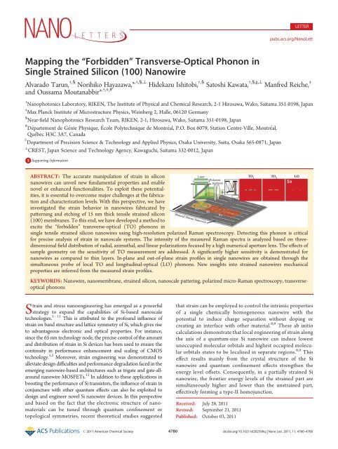
LETTER<br />
pubs.acs.org/NanoLett<br />
<strong>Mapping</strong> <strong>the</strong> <strong>“Forbid<strong>de</strong>n”</strong> Transverse-Optical Phonon in<br />
Single Strained Silicon (100) Nanowire<br />
Alvarado Tarun, †,§ Norihiko Hayazawa,* ,†,§,^ Hi<strong>de</strong>kazu Ishitobi, †,§ Satoshi Kawata, †,§,||,^ Manfred Reiche, ‡<br />
and Oussama Moutanabbir* ,†,‡,#<br />
† Nanophotonics Laboratory, RIKEN, The Institute of Physical and Chemical Research, 2-1 Hirosawa, Wako, Saitama 351-0198, Japan<br />
‡ Max Planck Institute of Microstructure Physics, Weinberg 2, Halle, 06120 Germany<br />
§ Near-field Nanophotonics Research Team, RIKEN, 2-1, Hirosawa, Wako, Saitama 351-0198, Japan<br />
# Departement <strong>de</strong> Genie Physique, Ecole <strong>Polytechnique</strong> <strong>de</strong> Montreal, P.O. Box 6079, Station Centre-Ville, Montreal,<br />
Quebec H3C 3A7, Canada<br />
^CREST,<br />
Department of Precision Science & Technology and Applied Physics, Osaka University, Suita, Osaka 565-0871, Japan<br />
Japan Science and Technology Agency, Kawaguchi, Saitama 332-0012, Japan<br />
)<br />
bS Supporting Information<br />
ABSTRACT: The accurate manipulation of strain in silicon<br />
nanowires can unveil new fundamental properties and enable<br />
novel or enhanced functionalities. To exploit <strong>the</strong>se potentialities,<br />
it is essential to overcome major challenges at <strong>the</strong> fabrication<br />
and characterization levels. With this perspective, we have<br />
investigated <strong>the</strong> strain behavior in nanowires fabricated by<br />
patterning and etching of 15 nm thick tensile strained silicon<br />
(100) membranes. To this end, we have <strong>de</strong>veloped a method to<br />
excite <strong>the</strong> “forbid<strong>de</strong>n” transverse-optical (TO) phonons in<br />
single tensile strained silicon nanowires using high-resolution polarized Raman spectroscopy. Detecting this phonon is critical<br />
for precise analysis of strain in nanoscale systems. The intensity of <strong>the</strong> measured Raman spectra is analyzed based on threedimensional<br />
field distribution of radial, azimuthal, and linear polarizations focused by a high numerical aperture lens. The effects of<br />
sample geometry on <strong>the</strong> sensitivity of TO measurement are addressed. A significantly higher sensitivity is <strong>de</strong>monstrated for<br />
nanowires as compared to thin layers. In-plane and out-of-plane strain profiles in single nanowires are obtained through <strong>the</strong><br />
simultaneous probe of local TO and longitudinal-optical (LO) phonons. New insights into strained nanowires mechanical<br />
properties are inferred from <strong>the</strong> measured strain profiles.<br />
KEYWORDS: Nanowire, nanomembrane, strained silicon, nanoscale pattering, polarized micro-Raman spectroscopy, transverseoptical<br />
phonons<br />
Strain and stress nanoengineering has emerged as a powerful<br />
strategy to expand <strong>the</strong> capabilities of Si-based nanoscale<br />
technologies. 1 11 This is attributed to <strong>the</strong> profound influence of<br />
strain on band structure and lattice symmetry of Si, which gives rise<br />
to advantageous electronic and optical properties. For instance,<br />
since <strong>the</strong> 65 nm technology no<strong>de</strong>, <strong>the</strong> precise control of <strong>the</strong> amount<br />
and distribution of strain in Si <strong>de</strong>vices has been used to ensure <strong>the</strong><br />
continuity in performance enhancement and scaling of CMOS<br />
technology. 1,2 Moreover, strain engineering was <strong>de</strong>monstrated to<br />
alleviate <strong>de</strong>sign difficulties and performance <strong>de</strong>gradation faced in <strong>the</strong><br />
emerging nanowire-based architectures such as trigate and gate-allaround<br />
nanowire MOSFETs. 11 In addition to <strong>the</strong>se applications in<br />
boosting <strong>the</strong> performance of Si transistors, <strong>the</strong> influence of strain in<br />
conjuncture with o<strong>the</strong>r quantum effects can also be exploited to<br />
<strong>de</strong>sign and engineer novel Si nanowire <strong>de</strong>vices. In this perspective<br />
and based on <strong>the</strong> fact that <strong>the</strong> electronic structure of nanomaterials<br />
can be tuned through quantum confinement or<br />
topological symmetries, recent <strong>the</strong>oretical studies suggested<br />
that strain can be employed to control <strong>the</strong> intrinsic properties<br />
of a single chemically homogeneous nanowire with <strong>the</strong><br />
potential to induce charge separation without doping or<br />
creating an interface with o<strong>the</strong>r material. 8,9 These ab initio<br />
calculations <strong>de</strong>monstrate that local engineering of strain along<br />
<strong>the</strong> axis of a quantum-size Si nanowire can induce lowest<br />
unoccupied molecular orbitals and highest occupied molecular<br />
orbitals states to be localized in separate regions. 8,9 This<br />
effect results mainly from <strong>the</strong> crystal structure of <strong>the</strong> Si<br />
nanowire and quantum confinement effects streng<strong>the</strong>n <strong>the</strong><br />
energy level offsets. Consequently, in a partially strained Si<br />
nanowire, <strong>the</strong> frontier energy levels of <strong>the</strong> strained part are<br />
simultaneously higher and lower than <strong>the</strong> unstrained part,<br />
effectively forming a type-II homojunction.<br />
Received: July 28, 2011<br />
Revised: September 21, 2011<br />
Published: October 03, 2011<br />
r 2011 American Chemical Society 4780 dx.doi.org/10.1021/nl202599q | Nano Lett. 2011, 11, 4780–4788
Nano Letters<br />
LETTER<br />
Figure 1. Schematic illustration of <strong>the</strong> process flow for <strong>the</strong> fabrication of background-free UT-SSOI using thin layer transfer. (a) Growth of relaxed<br />
Si 0.82 Ge 0.18 relaxed buffer layer on Si(100) substrate; (b) growth of biaxially tensile strained Si on Si 0.82 Ge 0.18 and subsequent hydrogen ion implantation<br />
into <strong>the</strong> grown heterostructure; (c) bonding of <strong>the</strong> hydrogen-implanted onto a host substrate on which Ge layer was grown followed by <strong>de</strong>position of<br />
SiO 2 layer; (d) <strong>the</strong>rmal annealing-induced layer exfoliation around <strong>the</strong> hydrogen implantation <strong>de</strong>pth; (e) cross-section transmission electron<br />
microscopy image of <strong>the</strong> heterostructure obtained after <strong>the</strong> removal of <strong>the</strong> residual SiGe. Inset: high-resolution image of <strong>the</strong> 15 nm thin strained<br />
membrane and <strong>the</strong> corresponding diffraction pattern. (f) Scanning electron microscopy of <strong>the</strong> array of nanowires fabricated by electron beam<br />
lithography and reactive ion etching. The thickness, <strong>the</strong> width, and <strong>the</strong> length of <strong>the</strong> nanowires are 15 nm, 30 nm, and 1 μm, respectively.<br />
The exploitation of <strong>the</strong> full potential of strain-engineered Si<br />
nanowire <strong>de</strong>vices raises two major challenges. First, <strong>the</strong> precise<br />
control of strain during <strong>the</strong> fabrication process remains an outstanding<br />
task, which becomes even more difficult for quantumsize<br />
nanowires. Several processes have been proposed so far<br />
including <strong>the</strong> realization of germanium silicon core shell<br />
nanowires syn<strong>the</strong>sized through metal-catalyzed vapor phase<br />
epitaxy. 3 This process is, however, associated with a number of<br />
un<strong>de</strong>sired morphological instabilities. 12 The use of local stressors<br />
such as SiGe alloys and Si nitri<strong>de</strong> lines can also be used to<br />
introduce strain, but this method can hardly be scaled as<br />
dimensions shrink. 13 The second challenge is related to <strong>de</strong>velopment<br />
of accurate, less invasive, and sensitive techniques to<br />
probe on <strong>the</strong> nanoscale <strong>the</strong> strain and <strong>the</strong> associated changes in<br />
<strong>the</strong> nanowire properties. A number of techniques have been<br />
proposed to measure <strong>the</strong> amount and distribution of strain in Si<br />
nanoscale systems. 14 19 However, each of <strong>the</strong>se techniques<br />
suffers a number of limitations such as being invasive or<br />
insensitive to all strain components, or having a limited spatial<br />
resolution. Tip-enhanced Raman spectroscopy is one of <strong>the</strong><br />
promising techniques to investigate <strong>the</strong> strain distribution in<br />
<strong>the</strong> nanoscale, 15,20 however, <strong>the</strong> electric polarization condition<br />
around <strong>the</strong> tip-apex has not been well characterized as it<br />
strongly <strong>de</strong>pends on <strong>the</strong> tip geometry and light illumination<br />
method.<br />
In this work, we utilized ultrathin tensile strained silicon-oninsulator<br />
(UT-SSOI) membranes to fabricate strained Si nanowires<br />
using a top-down approach. The local strain and <strong>the</strong><br />
involved free surface-induced strain redistribution during <strong>the</strong><br />
formation of <strong>the</strong> nanowire are investigated using high-resolution<br />
polarized micro-Raman spectroscopy. We <strong>de</strong>scribe a method that<br />
permits <strong>the</strong> excitation of <strong>the</strong> “forbid<strong>de</strong>n” transverse-optical (TO)<br />
phonons, which is critical for an accurate analysis of <strong>the</strong> strain in<br />
ultrathin strained Si nanowires. In-plane and out-of-plane strain<br />
profiles in single nanowires are obtained through this simultaneous<br />
probe of local longitudinal-optical (LO) and TO phonons.<br />
The profile of strain associated with TO Raman shifts across<br />
individual strained nanowires is analyzed and compared to LO<br />
related shifts. The intensity of <strong>the</strong> measured Raman spectra is<br />
analyzed based on three-dimensional field distribution of radial,<br />
azimuthal, and linear polarizations focused by a high numerical<br />
aperture (NA) lens. The effects of sample geometry on <strong>the</strong><br />
sensitivity of TO measurement are consi<strong>de</strong>red. New insights into<br />
strained nanowires mechanical properties are also discussed<br />
based on <strong>the</strong> measured strain profiles.<br />
Fabrication of Ultrathin Tensile Strained Si Nanowires.<br />
Figure 1a d illustrates <strong>the</strong> process employed to fabricate UT-<br />
SSOI membranes. The 15 nm thick strained Si membranes were<br />
generated by <strong>the</strong> epitaxial growth of Si on ∼500 nm thick<br />
Si 1‐x Ge x (x ∼ 0.18) relaxed buffer layers <strong>de</strong>posited on Si(001)<br />
substrate. Using direct wafer bonding and ion-cut process, 21 <strong>the</strong><br />
strained membrane was <strong>the</strong>n transferred onto a handle substrate<br />
capped with ∼120 nm thick layer of Ge grown by molecular<br />
beam epitaxy. Prior to direct bonding, both substrates were<br />
covered by a plasma-enhanced chemical vapor <strong>de</strong>posited SiO y<br />
layer. Figure 1e shows a cross-sectional transmission electron<br />
microscopy of <strong>the</strong> obtained structure with <strong>the</strong> Ge interlayer.<br />
Or<strong>de</strong>red arrays of strained Si nanowires were fabricated using<br />
<strong>the</strong>se UT-SSOI membranes by combining electron beam lithography<br />
(JEOL JBX-6300) and reactive ion etching. The etching<br />
process was carried out at a temperature of 60 °C in a mixture<br />
of SF 6 (100 sccm) and O 2 (5 sccm) at a power of 40 W. The<br />
etching conditions were optimized to avoid damage at <strong>the</strong> newly<br />
formed nanowire edges. The investigated nanowires have a<br />
length of 1 μm and a diameter of 30 nm (Figure 1f). All <strong>the</strong><br />
nanowires are aligned along <strong>the</strong> [110] direction and separated by<br />
4781 dx.doi.org/10.1021/nl202599q |Nano Lett. 2011, 11, 4780–4788
Nano Letters<br />
∼500 nm from each o<strong>the</strong>r. The introduction of a highly<br />
absorptive Ge layer un<strong>de</strong>rneath <strong>the</strong> buried oxi<strong>de</strong> was used to<br />
suppress <strong>the</strong> Si substrate background during Raman analysis 22<br />
(see Figure S1 in Supporting Information). Using this material,<br />
only vibrational mo<strong>de</strong>s intrinsic to strained nanowires are<br />
<strong>de</strong>tected. The Ge Ge peak 23 centered at 301.0 cm 1 is far from<br />
interfering with <strong>the</strong> Si Si peak of <strong>the</strong> strained membrane. This<br />
peak is insensitive to <strong>the</strong> stress in <strong>the</strong> SSOI and can be used as<br />
“wavenumber calibration” for Raman analysis as instabilities may<br />
occur during <strong>the</strong> experiment. For instance, slight changes in <strong>the</strong><br />
light pass may result in a shift of <strong>the</strong> strained Si peak. These<br />
minute changes are caused by <strong>the</strong> polarizers, analyzers, and o<strong>the</strong>r<br />
optics associated with micro-Raman spectroscopy techniques<br />
and/or small changes in <strong>the</strong> focusing of <strong>the</strong> laser on <strong>the</strong> sample<br />
during scanning. These instabilities could make <strong>the</strong> strain<br />
analysis fraught with large uncertainties.<br />
Methodology of TO Phonon Excitation in Strained Si<br />
Nanowire. Though imaging with only LO phonon is enough<br />
to obtain <strong>the</strong> in-plane strain distribution, Raman shifts from TO<br />
phonon are required for a more accurate characterization of<br />
strain. In<strong>de</strong>ed, <strong>the</strong> simultaneous probe of LO and TO phonons is<br />
of compelling importance to estimate both in-plane and out-ofplane<br />
strains. These quantities are critical to predict and control<br />
hole and electron relative mobility, which are related to vertical<br />
and lateral stress distributions. 24 In conventional backscattering<br />
geometry, <strong>the</strong> <strong>de</strong>tection of Si(001) Raman scattering from TO<br />
phonon is generally forbid<strong>de</strong>n. However, this is not <strong>the</strong> case<br />
when using high NA objective lens in terms of both excitation<br />
and <strong>de</strong>tection of TO phonons. In an early report, Brunner et al. 25<br />
have observed weak symmetry forbid<strong>de</strong>n phonon mo<strong>de</strong>s in<br />
compressively strained Si film using polarized Raman spectroscopy<br />
un<strong>de</strong>r backscattering configuration with an objective lens<br />
having a NA of 0.95. Additionally, TO phonons can, in principle,<br />
be measured with off-axis 26,27 (oblique) polarized Raman spectroscopy<br />
or when <strong>the</strong> sample is not (001)-oriented. 28 Therefore,<br />
it is important to note <strong>the</strong> excitation of TO phonons in Si(001)<br />
cannot be restricted in micro-Raman spectroscopy analysis even<br />
un<strong>de</strong>r <strong>the</strong> backscattering configuration. 25,29,30 In<strong>de</strong>ed, TO phonon<br />
in strained Si(001) films un<strong>de</strong>r <strong>the</strong> backscattering configuration<br />
was recently excited and <strong>de</strong>tected using linearly<br />
x-polarized light (parallel to <strong>the</strong> surface) focused with a high<br />
numerical aperture (NA) lens. 31,32 This is because <strong>the</strong> z-polarized<br />
component (longitudinal field) of focused light, which<br />
excites TO phonons, can be effectively generated using a high<br />
NA lens. However, y-polarized component, which is often<br />
ignored when using a linearly x-polarized excitation, is no longer<br />
negligible when a high NA lens is used due to <strong>de</strong>polarization<br />
effect. This <strong>de</strong>polarization effect at <strong>the</strong> diffraction-limited focus<br />
spot is consi<strong>de</strong>red in our analysis. The coexistence of LO phonon<br />
contribution in Raman signal due to y-polarized component,<br />
which cannot be suppressed by <strong>the</strong> analyzer during TO phonons<br />
measurement, reduces <strong>the</strong> accuracy of <strong>the</strong> technique. In this<br />
work, <strong>the</strong> effect of <strong>de</strong>polarization at focus generated by a high NA<br />
lens of different inci<strong>de</strong>nt polarizations on <strong>the</strong> sensitivity and<br />
accuracy of TO phonons excitation is investigated. The relative<br />
intensities of TO and LO Raman mo<strong>de</strong>s have been taken into<br />
consi<strong>de</strong>ration to accurately interpret <strong>the</strong> Raman data of strained<br />
Si nanowires. Notwithstanding <strong>the</strong> numerous attempts to excite<br />
and <strong>de</strong>tect TO phonons, 25 32 our work presents <strong>the</strong> first<br />
experimental investigation of TO-related strain behavior in<br />
individual nanostructures. It is also worth mentioning that <strong>the</strong><br />
xy-polarized component (transverse field) of <strong>the</strong> focus light can<br />
LETTER<br />
also excite TO phonons but <strong>the</strong> <strong>de</strong>tection efficiency is generally<br />
too small since <strong>the</strong> radiation dipole is oriented normal to <strong>the</strong><br />
surface. The electric field intensity distributions from a tightly<br />
focused lens is first calculated at different inci<strong>de</strong>nt polarizations<br />
and <strong>the</strong>n operated to <strong>the</strong> Si Raman tensor to estimate <strong>the</strong> Raman<br />
intensities of LO and TO optical phonons. Using a circular mask<br />
to block low NA components of <strong>the</strong> lens, radial, azimuthal, and<br />
linear polarizations are investigated.<br />
Polarized micro-Raman measurement was carried out in<br />
backscattering configuration using a modified inverted optical<br />
microscope with a PZT driven xy stage 33 (see Figure S2 in<br />
Supporting Information). The polarization of <strong>the</strong> expan<strong>de</strong>d<br />
inci<strong>de</strong>nt beam, ∼15, from 532 nm laser was controlled via<br />
combination of a polarizer, half-waveplate and an 8-segmented<br />
radial-waveplate (Zpol: Nanophoton Inc.). 34 Focusing <strong>the</strong> radial<br />
and azimuthal light by a high NA lens generates a strong<br />
longitudinal (z-polarized) and pure transverse (xy-polarized)<br />
electric field, respectively. Radial or azimuthal light can be easily<br />
obtained by properly selecting <strong>the</strong> polarization of <strong>the</strong> inci<strong>de</strong>nt<br />
light using <strong>the</strong> half-waveplate. Removing <strong>the</strong> radial-waveplate<br />
provi<strong>de</strong>s <strong>the</strong> linear polarization. The polarization-controlled<br />
inci<strong>de</strong>nt light passed through a circular mask to reject <strong>the</strong> low<br />
NA component (NA < 1) and was <strong>the</strong>n focused by a high NA<br />
(= 1.4), oil immersion lens. The mask is used to enhance <strong>the</strong><br />
z-component. The backscattered Raman signal was collected by<br />
<strong>the</strong> same objective lens and <strong>de</strong>livered to an analyzer before being<br />
recor<strong>de</strong>d by a spectrometer equipped with a liquid nitrogencooled<br />
charged couple <strong>de</strong>vice camera (CCD). The experimentally<br />
obtained wavelength repeatability and accuracy using Lorentzian<br />
fitting is ∼0.02 cm 1 . This was obtained by calculating<br />
<strong>the</strong> standard <strong>de</strong>viation from 10 Raman measurements. The<br />
system spectral resolution (grating = 1800 g/mm, focal length =<br />
640 mm, slit width = 100 μm) is ∼0.02 nm. The accuracy and<br />
sensitivity of our Raman analysis were confirmed using highresolution<br />
transmission electron microscoy-based methods. Collection<br />
of Raman signal uses <strong>the</strong> full NA of <strong>the</strong> lens. For <strong>the</strong> linear<br />
polarization experiment, <strong>the</strong> inci<strong>de</strong>nt light was x-polarized<br />
parallel to <strong>the</strong> length of <strong>the</strong> nanowire, which is in <strong>the</strong> [110]<br />
direction (See Figure S2 in Supporting Information), and <strong>the</strong><br />
scattered light was analyzed parallel and perpendicular to <strong>the</strong><br />
nanowire axis. The nanowire affixed on <strong>the</strong> xy translation stage<br />
was scanned with a step size of 50 nm (accuracy of 1.5 nm). At<br />
each step, <strong>the</strong> scattered Raman spectrum was recor<strong>de</strong>d at<br />
different combinations of inci<strong>de</strong>nt polarization and analyzer<br />
orientation relative to a fixed nanowire azimuth. A single Lorentz<br />
function was fitted to <strong>the</strong> Raman spectrum obtained using linear<br />
polarization, z(x,x)z setting (LO-active), to <strong>de</strong>termine <strong>the</strong> peak<br />
frequency of LO phonons. On <strong>the</strong> o<strong>the</strong>r hand, a double Lorentz<br />
fit function was applied for z(x,y)z setting (TO-active) to<br />
<strong>de</strong>compose and <strong>de</strong>termine <strong>the</strong> peak frequency of TO phonons.<br />
As <strong>de</strong>monstrated below, this is justified by <strong>the</strong> coexistence of<br />
both LO and TO phonons in <strong>the</strong> obtained spectrum. It should be<br />
stressed that during double Lorentzian fitting, <strong>the</strong> LO peak<br />
position was fixed and assumed equal to <strong>the</strong> value obtained from<br />
<strong>the</strong> single Lorentzian fitofz(x,x)z setting. This was done at each<br />
position in <strong>the</strong> nanowire simply because <strong>the</strong> LO phonon peak<br />
position varies along <strong>the</strong> nanowire due to <strong>the</strong> nonuniform<br />
distribution of strain. Likewise, single and double Lorentzian<br />
fittings were applied for <strong>the</strong> inci<strong>de</strong>nt azimuthal and radial<br />
polarization, respectively. This is because azimuthal polarization<br />
<strong>de</strong>tects mostly LO phonon while radial polarization excites and<br />
<strong>de</strong>tects both LO and TO phonons. In <strong>the</strong> double Lorentzian fitof<br />
4782 dx.doi.org/10.1021/nl202599q |Nano Lett. 2011, 11, 4780–4788
Nano Letters<br />
radial polarization, <strong>the</strong> LO peak value was fixed and takes <strong>the</strong><br />
value obtained from <strong>the</strong> single Lorentzian fit of <strong>the</strong> azimuthal<br />
polarization. An exposure time of 120 and 30 s at 145 μW power<br />
was used for TO-active and LO-active condition, respectively. At<br />
this experimental condition, we ma<strong>de</strong> sure that heating due to<br />
laser energy is negligible by systemically analyzing <strong>the</strong> measured<br />
signals as a function of <strong>the</strong> laser power in <strong>the</strong> range of 31 316<br />
μW. 35 It is also worth mentioning that <strong>the</strong> dimensions of strained<br />
Si nanowires (thickness = 15 nm and width = 30 nm) are large<br />
enough to prevent phonon confinement effects. 35,36<br />
The scattering efficiency, I, <strong>de</strong>pends on <strong>the</strong> polarization vector<br />
of both <strong>the</strong> inci<strong>de</strong>nt (e i ) and <strong>the</strong> scattered (e s ) light, and is<br />
generally expressed as 37<br />
I µ ∑ je T s R je i j 2<br />
ð1Þ<br />
j<br />
where R j is <strong>the</strong> Raman polarizability tensor for j th active phonon<br />
mo<strong>de</strong> and e i and e s are <strong>the</strong> inci<strong>de</strong>nt and scattered electric field<br />
unit vectors, respectively. The superscript T <strong>de</strong>notes transpose of<br />
<strong>the</strong> scattered electric field vector. The Raman tensor for Si in <strong>the</strong><br />
absence of stress is <strong>de</strong>rived by Loudon 37 and expressed in crystal<br />
coordinate system X=[100], Y=[010] and Z=[001]. They are<br />
given by<br />
0 1 0 1<br />
0 0 0<br />
0 0 d<br />
R X ¼<br />
B<br />
@ 0 0 d C<br />
A, R Y ¼<br />
B 0 0 0C<br />
@ A,<br />
0 d 0<br />
d 0 0<br />
0 1<br />
0 d 0<br />
R Z ¼<br />
B d 0 0C<br />
@ A<br />
0 0 0<br />
ð2Þ<br />
where d is a constant that is <strong>de</strong>pen<strong>de</strong>nt on <strong>the</strong> Raman polarizability<br />
of <strong>the</strong> sample. For backscattering from a (001) surface, R X<br />
and R Y are <strong>the</strong> Raman tensor by <strong>the</strong> TO 1 and TO 2 , respectively,<br />
whereas R Z corresponds to LO phonons. In or<strong>de</strong>r to accurately<br />
obtain <strong>the</strong> contributions from LO and TO, we quantitatively<br />
compare <strong>the</strong> intensities of LO and TO phonons at different<br />
inci<strong>de</strong>nt polarizations (linear, radial, and azimuthal) using a high<br />
NA lens. Since <strong>the</strong> edges of <strong>the</strong> nanowire are aligned along [110]<br />
direction, <strong>the</strong> Si Raman tensor in <strong>the</strong> crystal axes (XYZ) needs to<br />
be transformed in <strong>the</strong> sample coordinate (xyz) axes using tensor<br />
rotation. The Raman tensor in <strong>the</strong> sample coordinate axes is 38<br />
0 1<br />
0<br />
1<br />
R 0 x ¼ p<br />
1 0 0 d<br />
ffiffi<br />
B 0 0 d C<br />
@ A, R 0 y<br />
2<br />
¼ 1 0 0 d<br />
pffiffi<br />
B 0 0 d C<br />
@<br />
A,<br />
d d 0<br />
2<br />
d d 0<br />
0 1<br />
d 0 0<br />
R 0 z ¼ B 0 d 0 C<br />
@ A<br />
ð3Þ<br />
0 0 0<br />
In <strong>the</strong> typical backscattering configuration of most microscopes,<br />
<strong>the</strong> z-axis is taken as <strong>the</strong> laser beam propagation direction,<br />
while <strong>the</strong> analyzer, e s , polarization direction takes ei<strong>the</strong>r x- or<br />
y-axis. In this work, we utilized a high NA lens to take advantage<br />
of <strong>the</strong> higher z-component of light at <strong>the</strong> focus. On <strong>the</strong> basis of<br />
<strong>the</strong> Raman polarization selection rules, 28,38 this z-polarized light<br />
excites <strong>the</strong> TO phonons. However, as we increase <strong>the</strong> NA of <strong>the</strong><br />
lens, <strong>the</strong> <strong>de</strong>polarized (y-component) light at <strong>the</strong> focus also<br />
LETTER<br />
increases and becomes comparable to <strong>the</strong> z-component for<br />
linearly x-polarized inci<strong>de</strong>nt light. 39 This contribution from<br />
<strong>de</strong>polarized light cannot be eliminated when scattered Raman<br />
is analyzed as in <strong>the</strong> case of polarized micro-Raman measurements,<br />
that is, z(x, y)z. In or<strong>de</strong>r to <strong>de</strong>scribe <strong>the</strong> scattering process<br />
that involves illumination and collection by high NA lens, we<br />
cannot assume e i to be constant across <strong>the</strong> focal volume. In <strong>the</strong><br />
focus, <strong>the</strong> polarization of light has components along x, y, and z. 40<br />
For instance, in <strong>the</strong> z(x, y)z setting, <strong>the</strong> excited LO phonon<br />
arising from <strong>the</strong> generated <strong>de</strong>polarized (y-polarized) field overlaps<br />
with <strong>the</strong> TO phonon resulting from <strong>the</strong> created longitudinal<br />
(z-polarized) field. To take into account <strong>the</strong> effects of <strong>the</strong> x, y, and<br />
z-components of <strong>the</strong> light on <strong>the</strong> intensity of <strong>de</strong>tected Raman,<br />
numerical calculations aimed to <strong>de</strong>termine <strong>the</strong> electric field<br />
intensity (|e i | 2 ) distributions from a tightly focused lens were<br />
performed for 15 nm thick strained Si membrane. The resulting<br />
values are operated to <strong>the</strong> transformed Si Raman tensor to<br />
estimate <strong>the</strong> Raman intensities of LO and TO phonons. Ano<strong>the</strong>r<br />
factor we need to examine is <strong>the</strong> change in <strong>the</strong> amplitu<strong>de</strong> of <strong>the</strong><br />
x- and y-polarized light during laser focusing into Si membrane,<br />
which has a very high refractive in<strong>de</strong>x comparable to bulk silicon<br />
(n = 4.15 + 0.043i at 532 nm). 41 This change in <strong>the</strong> amplitu<strong>de</strong> of<br />
<strong>the</strong> x- and y-polarized light can be easily taken into account by<br />
calculating <strong>the</strong> Fresnel equations in or<strong>de</strong>r to obtain <strong>the</strong> transmission<br />
and reflection coefficients of p- and s-polarized light at<br />
different media of known refractive in<strong>de</strong>x. 42 In this particular<br />
experiment, light propagates into a three-layer system consisting<br />
of oil (0th from oil-immersion objective lens), strained-Si (1st)<br />
and SiO 2 (2nd). These Fresnel coefficients were calculated by<br />
taking into account <strong>the</strong> multiple reflections at oil/strained Si and<br />
strained Si/SiO 2 interfaces. We neglect <strong>the</strong> contributions from<br />
<strong>the</strong> highly absorptive Ge-layer in <strong>the</strong> mo<strong>de</strong>l because <strong>the</strong> polarized<br />
micro-Raman setup is confocal and that <strong>the</strong> multiple reflections<br />
from Ge-layer are assumed to be small due to <strong>the</strong> high refractive<br />
in<strong>de</strong>x of Ge. To mo<strong>de</strong>l <strong>the</strong> effect of <strong>the</strong> high NA lens used for<br />
illumination on <strong>the</strong> Raman spectrum, we numerically calculated<br />
<strong>the</strong> (|e i | 2 ) over <strong>the</strong> finite solid angle subten<strong>de</strong>d by <strong>the</strong> objective.<br />
Hence, to integrate all <strong>the</strong> non-negligible effects discussed above<br />
on <strong>the</strong> intensity of <strong>the</strong> Raman mo<strong>de</strong>, eq 1 can be replaced by<br />
2 0<br />
13<br />
I i ¼ I 0 ∑<br />
i<br />
Z 2π Z θmax<br />
0<br />
0<br />
E scaX ðθ, ϕ, ηÞ<br />
6<br />
Rðα, β, γÞ<br />
B E scaY ðθ, ϕ, ηÞ C7<br />
<br />
4 @<br />
A5<br />
E scaZ ðθ, ϕ, ηÞ<br />
2<br />
0 13<br />
E x<br />
2<br />
<br />
6<br />
R i 3 Rðα, β, γÞ B<br />
@ E C7<br />
4<br />
y A5<br />
sin θdθdϕ<br />
<br />
E z<br />
T<br />
ð4Þ<br />
where, I 0 is <strong>the</strong> inci<strong>de</strong>nt intensity, η is <strong>the</strong> angle setting of <strong>the</strong><br />
analyzer with respect to <strong>the</strong> x-axis, and θ and ϕ are <strong>the</strong> polar and<br />
azimuthal angles. The explicit form of E x , E y , and E z <strong>de</strong>pends on<br />
whe<strong>the</strong>r radial, azimuthal, or linear inci<strong>de</strong>nt polarization is used<br />
(see Supporting Information, Section A). E sca (ϕ,θ,η) is <strong>the</strong><br />
scattered electric field <strong>de</strong>fined from <strong>the</strong> objective transfer matrix<br />
that <strong>de</strong>scribes <strong>the</strong> radiation dipole collection efficiency of a high<br />
NA objective lens (See Supporting Information, Section A). R i<br />
is <strong>the</strong> Raman tensor in <strong>the</strong> crystal coordinate (XYZ) system,<br />
which can be easily transformed into sample coordinate (xyz)<br />
system using <strong>the</strong> well-known Euler rotation matrix, 43 R(α,β,γ)<br />
4783 dx.doi.org/10.1021/nl202599q |Nano Lett. 2011, 11, 4780–4788
Nano Letters<br />
LETTER<br />
Figure 2. (a) Electric field distribution on <strong>the</strong> surface of <strong>the</strong> strained Si membrane and <strong>the</strong> corresponding calculated Raman intensities (normalized at<br />
each setting) using eq 4 at various analyzer and polarizer settings. Image size is 1 1 μm 2 . For each setting, <strong>the</strong> TO/LO Raman intensities were<br />
calculated in three-dimensional (3D) and tabulated. Note: The observed maximum Raman intensity is found at <strong>the</strong> SiO 2 and strained Si interface.<br />
(b) Raman spectra measured from <strong>the</strong> strained membrane at different experimental configurations. (c) Comparison between numerical and<br />
experimental normalized total intensities obtained from panels a and b.<br />
(see Supporting Information Section C). The integration over<br />
<strong>the</strong> solid angle, sin θ dθdϕ, is confined only to <strong>the</strong> collection cone<br />
for <strong>the</strong> scattered light. This scattered intensity is a complex function<br />
whose explicit form is <strong>de</strong>termined by <strong>the</strong> Raman polarizability<br />
tensors. In <strong>the</strong> absence of stress, <strong>the</strong> three optical phonons<br />
of Si have <strong>the</strong> same frequency (<strong>de</strong>generate). 28 However, in <strong>the</strong><br />
presence of stress, <strong>the</strong>se Raman mo<strong>de</strong>s lift <strong>the</strong>ir <strong>de</strong>generacy. Therefore,<br />
asi<strong>de</strong> from <strong>the</strong> changes in <strong>the</strong> intensity of <strong>the</strong> Raman mo<strong>de</strong>,<br />
variations in <strong>the</strong> frequency of LO and TO phonons can be analyzed.<br />
LO and TO phonons in UT-SSOI membrane. Figure 2a<br />
shows <strong>the</strong> numerically obtained 1 1 μm 2 electric field<br />
distributions at <strong>the</strong> surface of strained Si at different polarizations.<br />
These distributions were obtained for a 532 nm light<br />
source focused with a high NA (1.0 e NA e 1.4) oil lens (See<br />
Figure S2 in Supporting Information). The electric field distributions<br />
were normalized at each inci<strong>de</strong>nt polarization for<br />
comparison. For linearly x-polarized light, it can be seen that<br />
<strong>the</strong> <strong>de</strong>polarized, y-, and normal, z-components, are nonzero with<br />
comparable amplitu<strong>de</strong>. This suggests that for high NA illumination,<br />
<strong>the</strong> three Raman mo<strong>de</strong>s in eq 4 are excited. The excited<br />
Raman intensity of <strong>the</strong> three Raman mo<strong>de</strong>s <strong>de</strong>noted by TO 1 ,<br />
TO 2 , and LO can be <strong>de</strong>termined by operating <strong>the</strong> field distribution<br />
with <strong>the</strong> Raman tensor of Si at different analyzer settings as<br />
indicated in Figure 2a. Similar to electric field distribution, <strong>the</strong><br />
calculated excited Raman intensity for each analyzer setting was<br />
also normalized for <strong>the</strong> sake of clarity. The normalization is done<br />
relative to <strong>the</strong> maximum Raman intensity for each analyzer<br />
setting. In <strong>the</strong> case of Si nanomembrane (film), <strong>the</strong> Raman<br />
intensity is normalized to <strong>the</strong> maximum intensity of <strong>the</strong> excited<br />
LO signal for each analyzer setting. But in <strong>the</strong> case of nanowires,<br />
Raman intensity is normalized to maximum Raman intensity of<br />
ei<strong>the</strong>r TO 1 or LO signal. From this we note that <strong>the</strong> normalized<br />
LO intensity in z(x, x)z̅is of <strong>the</strong> same contrast as <strong>the</strong> normalized<br />
LO in <strong>the</strong> z(x, y)z ̅setting. The normalized TO intensity in <strong>the</strong><br />
z(x, x)z setting have <strong>the</strong> same intensity as normalized TO in <strong>the</strong><br />
z(x, y)z setting. Thus, <strong>the</strong> LO intensity is very strong compared<br />
to TO intensity even after scaling <strong>the</strong> value of TO to 20 times.<br />
When <strong>the</strong> analyzer is set parallel to y-axis (η = 90), TO and LO<br />
can be <strong>de</strong>tected simply because <strong>the</strong> strong LO excited by<br />
x-polarized light is mostly blocked by <strong>the</strong> analyzer. In polarized<br />
4784 dx.doi.org/10.1021/nl202599q |Nano Lett. 2011, 11, 4780–4788
Nano Letters<br />
micro-Raman spectroscopy un<strong>de</strong>r backscattering geometry, <strong>the</strong><br />
system setting <strong>de</strong>scribed above is represented as z(x, y)z in Porto<br />
notation. Though both z(x, x)z and z(x, y)z settings contain LO<br />
and TO mo<strong>de</strong>s, <strong>the</strong> TO/LO ratio difference between settings is<br />
significant. In <strong>the</strong> case of z(x, y)z, <strong>the</strong> TO/LO ratio is ∼0.90.<br />
On <strong>the</strong> o<strong>the</strong>r hand, for z(x, x)z, TO/LO ratio is ∼0.04. Owing to<br />
this, we <strong>de</strong>fine <strong>the</strong> z(x, y)z setting as TO-active and <strong>the</strong> z(x, x)z as<br />
LO-active. The TO/LO ratio is calculated by integrating <strong>the</strong><br />
intensity in three dimensions over <strong>the</strong> 15 nm thick UT-SSOI<br />
membrane and over <strong>the</strong> diffraction-limited focus spot, which is<br />
<strong>de</strong>fined by 1.22λ/NA (∼464 nm). For <strong>the</strong> radially polarized<br />
light, we can generate relatively higher z-components, ∼2, of<br />
<strong>the</strong> light compared to linear polarization. However, both x- and<br />
y-components have <strong>the</strong> same light intensity unlike in linear<br />
polarization where <strong>the</strong> <strong>de</strong>polarized light is weak and somewhat<br />
comparable to z-components. Never<strong>the</strong>less, radially polarized<br />
light can also be suitable for TO characterization because TO<br />
spatial resolution is approximately twice better as compared to<br />
linear polarization. The Raman intensity distribution of radially<br />
polarized light is tightly focused and locally observed at <strong>the</strong> center<br />
as opposed to <strong>the</strong> two intense split feature of <strong>the</strong> field distribution<br />
in <strong>the</strong> linear polarization. For azimuthal polarization, mostly LO<br />
mo<strong>de</strong> is <strong>de</strong>tectable because <strong>the</strong> z-components of <strong>the</strong> electric field<br />
are zero. Thus we <strong>de</strong>fine azimuthal polarization as LO-active and<br />
radial polarization as TO-active. The difference in <strong>the</strong> intensity of<br />
TO 1 and TO 2 in Figure 2a can be easily un<strong>de</strong>rstood from<br />
polarization selection rules. 28,37 In TO 2 , <strong>the</strong> generated Raman<br />
arising from <strong>the</strong> transverse electric fields cancels each o<strong>the</strong>r<br />
0<br />
because of <strong>the</strong> presence of negative sign in <strong>the</strong> Raman tensor, R y<br />
(See eq 3). In <strong>the</strong> case of TO 1 , <strong>the</strong> Raman signals excited from<br />
<strong>the</strong> transverse fields add up. Figure 2b shows some variations in<br />
<strong>the</strong> total Raman intensity at different experimental configurations.<br />
The total intensity (area un<strong>de</strong>r each Raman spectrum) was<br />
<strong>de</strong>termined and compared with numerically calculated intensity<br />
in Figure 2a. Figure 2b shows <strong>the</strong> Raman spectra from <strong>the</strong><br />
strained membrane at various inci<strong>de</strong>nt and scattered polarizations.<br />
The measured Si Si Raman peak was found to be centered<br />
at ∼514.3 cm 1 , about ∼6.2 cm 1 below its unstrained Si Si<br />
peak (gray vertical line) position, ∼520.5 cm 1 at room<br />
temperature. 44 The biaxial strain is estimated using 21<br />
ω ε Si ¼ ω Si þ 1 <br />
ω Si<br />
q þ<br />
<br />
S 12 ðεxx þ ε yy Þ<br />
p<br />
S 11 þ S 12 2<br />
ð5Þ<br />
where ε xx and ε yy are <strong>the</strong> two in-plane strain components, ω ε Si<br />
and ω Si are <strong>the</strong> Raman frequency shifts (in cm 1 ) of strained and<br />
unstrained Si, respectively. The S 11 = 7.68 and S 12 = 2.14<br />
(in GPa) are <strong>the</strong> elastic compliance tensor elements, while p =<br />
1.85 ω 2 Si and q = 2.31 ω 2 Si are <strong>the</strong> phonon <strong>de</strong>formation<br />
potentials for bulk Si. 45,46 The sensitivity and reliability of strain<br />
analysis based on eq 5 were confirmed using strained nanomemebranes<br />
with different strain levels and TEM-based methods.<br />
The corresponding biaxial tensile strain of ε xx = ε yy = 0.75% was<br />
estimated for <strong>the</strong> membrane. Figure 2c shows <strong>the</strong> comparison of<br />
<strong>the</strong> numerical and experimental results. Good agreement between<br />
<strong>the</strong> two sets of data is observed.<br />
LO and TO Phonon Profiles in Strained Si Nanowire. When<br />
characterizing strain in nanoscale <strong>de</strong>vices such as strained<br />
nanowires, it is very important to know <strong>the</strong> location of <strong>the</strong> peak<br />
position or high intensity areas of <strong>the</strong> E x , E y , and E z light<br />
components relative to <strong>the</strong> nanostructure. This is because <strong>the</strong><br />
<strong>de</strong>tected Raman can ei<strong>the</strong>r be LO or TO or a combination of<br />
LETTER<br />
both mo<strong>de</strong>s <strong>de</strong>pending on <strong>the</strong> location of <strong>the</strong> nanowire relative to<br />
<strong>the</strong> peak position of <strong>the</strong> field at <strong>the</strong> focus. From <strong>the</strong> calculations<br />
<strong>de</strong>scribed in Figure 2a, <strong>the</strong> best setting to obtain LO and TO<br />
optical phonon at <strong>the</strong> same position on <strong>the</strong> strained Si nanowire<br />
is to locate <strong>the</strong> nanowire at <strong>the</strong> center of <strong>the</strong> focus and first obtain<br />
LO peak position using z(x, x)z and <strong>the</strong>n switch to radial<br />
polarization by inserting <strong>the</strong> Z-pol to obtain <strong>the</strong> peak position<br />
of TO using z(rad, y)z setting. This is because <strong>the</strong> intense part of<br />
Raman intensity distributions for LO and TO are colocated at <strong>the</strong><br />
center of <strong>the</strong> focus for both <strong>the</strong> z(x, x)z and z(rad, y)z setting as<br />
indicated in Figure 2a.<br />
Figure 2a shows <strong>the</strong> calculated Raman distribution from TOactive,<br />
z(x, y)z and z(rad, y)z configuration for strained Si<br />
nanowire with lateral dimensions of 30 nm and 1 μm and a<br />
thickness of 15 nm. We can see that TO/LO ratio increases<br />
significantly for <strong>the</strong> nanowire un<strong>de</strong>r z(x, y)z and z(rad, y)z<br />
setting and reaches 126.81 and 8.10, respectively. This calculated<br />
TO/LO intensity ratio is one to 2 or<strong>de</strong>rs of magnitu<strong>de</strong> higher<br />
compared to <strong>the</strong> calculated ratio for <strong>the</strong> strained membrane. It is<br />
important to mention that <strong>the</strong> TO/LO ratio changes <strong>de</strong>pending<br />
on <strong>the</strong> width of <strong>the</strong> nanowire. Ano<strong>the</strong>r interesting observation is<br />
that <strong>the</strong> characterized area (strength and location of Raman peak<br />
intensities) along <strong>the</strong> nanowire between z(x, y)z and z(rad, y)z<br />
setting is different. The sensitivity of TO <strong>de</strong>tection un<strong>de</strong>r linear<br />
polarization is higher than radial polarization based on <strong>the</strong> TO/<br />
LO ratio. However, <strong>the</strong> strength of <strong>the</strong> TO Raman signal in radial<br />
polarization is higher than linear polarization at a fixed laser<br />
power. Hence, radial polarization is advantageous compared to<br />
linear polarization when low power is nee<strong>de</strong>d for TO characterization<br />
in strained nanowire. This is because nanowire heats up<br />
easily compared to <strong>the</strong> strained membrane.<br />
Figures 3a,b shows <strong>the</strong> measured Raman spectra at <strong>the</strong> center of a<br />
single UT-SSOI nanowire using z(x, y)z and z(rad, y)z settings,<br />
respectively. For comparison, <strong>the</strong> measured Raman from LO-active,<br />
z(x, y)z and z(azi, x)z,configurations were plotted. We can clearly<br />
see that <strong>the</strong> TO-active is broa<strong>de</strong>r than <strong>the</strong> LO-active condition for<br />
both radial and linear inci<strong>de</strong>nt polarizations (Note that <strong>the</strong> spectral<br />
accuracy for this analysis is ∼0.02 cm 1 ). This is because <strong>the</strong> TOactive<br />
condition consists of contributions from both LO and TO<br />
phonons. Note that <strong>the</strong> data presented is taken at <strong>the</strong> same laser<br />
power and that is not <strong>de</strong>convoluted with system spectral resolution<br />
and laser line width. The broa<strong>de</strong>ning of <strong>the</strong> Raman width can be<br />
interpreted as strain-<strong>de</strong>pen<strong>de</strong>nt overlap of <strong>the</strong> non<strong>de</strong>generate threephonon<br />
mo<strong>de</strong>s. The Si Si LO mo<strong>de</strong> peak position is centered at<br />
∼516.7 cm 1 ,whichis2.4cm 1 above <strong>the</strong> value in <strong>the</strong> initial<br />
membrane (∼514.3 cm 1 )inFigure2b(SeealsoFigureS4in<br />
Supporting Information). This strain relaxation is result of formation<br />
of free surfaces during patterning (RIE process). The obtained<br />
LO peak parameters in <strong>the</strong> z(x, x)z setting were utilized to fit<strong>the</strong>LO<br />
peak position in <strong>the</strong> double Lorentzian fitting of <strong>the</strong> measured<br />
spectra from z(x, y)z configuration to <strong>de</strong>termine <strong>the</strong> peak of Si Si<br />
TO phonons. We found that <strong>the</strong> Si Si TO peak position located at<br />
∼517.7 cm 1 (∼1.0 cm 1 blueshifted with respect to LO phonon)<br />
corresponding to lower strain. The TO/LO intensity ratio, obtained<br />
by integrating <strong>the</strong> Raman spectrum, was found to be 1.5 and 0.9 for<br />
z(x, y)z and z(rad, y)z settings, respectively. This measured TO/LO<br />
intensity ratio agrees qualitatively with <strong>the</strong> calculation in Figure 2a<br />
where <strong>the</strong> TO/LO ratio is higher in z(x, y)z than z(rad, y)z settings.<br />
The variation in <strong>the</strong> magnitu<strong>de</strong> of <strong>the</strong> measured TO/LO in<br />
Figure 3a,b to that of <strong>the</strong> calculated TO/LO in Figure 2a can be<br />
due to <strong>the</strong> alignment <strong>de</strong>viations, which is found to be very sensitive<br />
to <strong>the</strong> position and actual diameter of <strong>the</strong> UT-SSOI relative to <strong>the</strong><br />
4785 dx.doi.org/10.1021/nl202599q |Nano Lett. 2011, 11, 4780–4788
Nano Letters<br />
LETTER<br />
Figure 3. Raman spectra measured at <strong>the</strong> center of <strong>the</strong> nanowire for (a)<br />
z(x, y)z and (b) z(rad, y)z TO-active settings. For comparison, recor<strong>de</strong>d<br />
Raman spectra from LO-active, z(x, x)z and z(azi, x)z, were also plotted.<br />
The solid red (LO) and blue (TO) lines are <strong>the</strong> result of <strong>the</strong> double<br />
Lorentzian fit un<strong>de</strong>r <strong>the</strong> TO-active setting. The dashed red (LO) line is<br />
<strong>the</strong> fit of Raman peak un<strong>de</strong>r LO-active setting. The gray vertical lines<br />
<strong>de</strong>note Raman peak positions for bulk Si, LO, and TO phonons of<br />
strained silicon.<br />
center of <strong>the</strong> focus. Moreover, <strong>the</strong> variation can be partly attributed<br />
to <strong>the</strong> edges of <strong>the</strong> patterned structures, which are aligned along <strong>the</strong><br />
[110] direction. This is because for backscattering from (110)<br />
surface, ei<strong>the</strong>r <strong>the</strong> LO or <strong>the</strong> TO can be excited and <strong>de</strong>tected based<br />
on selection rules. 38<br />
Figure 4a shows <strong>the</strong> profiles of Si Si peak for TO (primary<br />
y-axis) and LO (secondary y-axis) along <strong>the</strong> nanowire at a 50 nm<br />
step. The gray bar in <strong>the</strong> plot presents <strong>the</strong> strained nanowire and can<br />
be used to correlate <strong>the</strong> measured Raman and <strong>the</strong> position on <strong>the</strong><br />
nanowire where data is obtained. The plotted data are <strong>the</strong> average<br />
from two scans across <strong>the</strong> length of <strong>the</strong> same nanowire un<strong>de</strong>r <strong>the</strong><br />
same experimental conditions. We observed that both LO and TO<br />
relaxations become more pronounced away from <strong>the</strong> center of <strong>the</strong><br />
nanowire. The difference in <strong>the</strong> behavior between linear and radial<br />
inci<strong>de</strong>nt polarizations can be due to both TO/LO sensitivity and<br />
spatial resolution associated with <strong>the</strong>m (see Figures 2a and 3a). For<br />
<strong>the</strong> linear setting, both TO and LO profiles display a plateau at 300<br />
e L e 700 nm, which means that <strong>the</strong> stress is nearly constant in this<br />
region. The stress <strong>the</strong>n drastically <strong>de</strong>creases toward <strong>the</strong> edges of <strong>the</strong><br />
nanowire. For radial setting, both TO and LO <strong>de</strong>crease monotonically<br />
and somewhat follows a parabolic behavior. The slight<br />
Figure 4. Profiles of TO peak (primary y-axis) and <strong>the</strong> LO peak<br />
(secondary y-axis) positions across <strong>the</strong> nanowire un<strong>de</strong>r (a) z(x, y)z<br />
and (b) z(rad, y)z TO-active settings. (c) Profile of <strong>the</strong> stressratio<br />
between singlet and doublet phonons along <strong>the</strong> nanowire. The<br />
x-position is parallel to <strong>the</strong> [110] direction. Horizontal line is <strong>the</strong><br />
<strong>the</strong>oretical value for stress ratio using eqs 6 and 7. The gray bar in <strong>the</strong><br />
plot presents <strong>the</strong> strained nanowire.<br />
difference in <strong>the</strong> TO profile between <strong>the</strong> two polarizations could be<br />
due <strong>the</strong> presence of two intense peaks in linear polarization versus<br />
single intense peak in radial polarization.<br />
For a strained nanowire, <strong>the</strong> actual stress along <strong>the</strong> σ xx and <strong>the</strong><br />
σ yy are generally not equal and vary with <strong>the</strong> width and length of<br />
<strong>the</strong> nanowire due to <strong>the</strong> edge-induced relaxation. 46 Note that <strong>the</strong><br />
strain remains biaxial but not bi-isotropic as it is in <strong>the</strong> initial<br />
strained membrane. The stress-induced Raman phonon shifts<br />
can be obtained by solving <strong>the</strong> well-known secular equation. 38 In<br />
<strong>the</strong> case of (001) in-plane biaxial tensile stress and with <strong>the</strong><br />
assumption that σ xx = σ yy = σ(xx [110], yy [110]) and σ zz =0<br />
(zz [001]), <strong>the</strong> stress-induced Raman shift for doublet (Δω d ,<br />
TO phonons) and singlet (Δω s , LO phonons) are<br />
)<br />
)<br />
)<br />
Δω d ¼ ½pðS 11 þ S 12 ÞþqðS 11 þ 3S 12 Šσ<br />
2ω 0<br />
¼ 3:42 σ ð6Þ<br />
Δω s ¼ ½pS 12 þ qðS 11 þ S 12 ÞŠσ<br />
ω 0<br />
¼ 4:60 σ ð7Þ<br />
4786 dx.doi.org/10.1021/nl202599q |Nano Lett. 2011, 11, 4780–4788
Nano Letters<br />
LETTER<br />
noticeable that <strong>the</strong> edges of <strong>the</strong> nanowire are more relaxed<br />
compared to <strong>the</strong> center. This behavior agrees with threedimensional<br />
finite element simulations of strain distribution in<br />
patterned nanowires (see Figure S5 in Supporting Information).<br />
To <strong>de</strong>scribe this evolution as well as <strong>the</strong> associated<br />
mechanical properties of <strong>the</strong> nanowire, we combine Hu’s<br />
mo<strong>de</strong>l 47 of stress relaxation and <strong>the</strong> analysis done by Fischer<br />
et al. 48 to fit <strong>the</strong> stress behavior shown in Figure 5. The stress<br />
distribution can be fitted using <strong>the</strong> equation below<br />
" rffiffiffiffiffiffiffiffi#<br />
" rffiffiffiffiffiffiffiffiffiffiffiffiffiffiffiffiffiffiffiffi#!<br />
2Kx<br />
2KðL xÞ<br />
σðxÞ ¼A 1 exp<br />
exp<br />
dπ<br />
dπ<br />
ð8Þ<br />
K ¼ E SiO 2<br />
ð1 ν 2 εSi Þ<br />
E εSi ð1 ν 2 and ðS 11 þ S 12 Þ¼ ð1 ν2 εSi Þ<br />
SiO 2<br />
Þ<br />
E εSi<br />
Figure 5. Profiles of LO and TO stress along <strong>the</strong> wire using (a) linear<br />
and (b) radial polarizations. The TO and LO stress were calculated from<br />
eqs 6 and 7, respectively. The x-position is parallel to <strong>the</strong> [110] direction.<br />
The solid curves are obtained by fitting eq 8. K is <strong>the</strong> relative rigidity of<br />
<strong>the</strong> nanowire, which is a function of Young’s modulus and Poisson ratio.<br />
where Δω d = ω ε Si ω 0 and Δω s = ω ε Si ω 0 are expressed<br />
in <strong>the</strong> Raman frequency in each mo<strong>de</strong> in <strong>the</strong> presence (ω ε Si )<br />
and <strong>the</strong> absence (ω 0 ) of stress. Using <strong>the</strong> phonon <strong>de</strong>formation<br />
potential and <strong>the</strong> compliance tensor element values, listed<br />
above (see eq 5 and refs 45 and 46), <strong>the</strong> <strong>the</strong>oretical stress ratio<br />
(Δω s /Δω d )is∼1.34. Figure 4c shows <strong>the</strong> variations in <strong>the</strong><br />
experimentally obtained stress ratio (Δω s /Δω d ) along <strong>the</strong><br />
nanowire for linear and radial polarizations. We can observe that<br />
<strong>the</strong> stress ratio at <strong>the</strong> edges of <strong>the</strong> nanowire approaches <strong>the</strong><br />
<strong>the</strong>oretical value (gray horizontal line) of 1.34. However, it starts<br />
to <strong>de</strong>viate away from <strong>the</strong> <strong>the</strong>oretical value as we approach <strong>the</strong><br />
center of <strong>the</strong> nanowire. The Δω s /Δω d value at regions far from<br />
<strong>the</strong> edges is lower relative to <strong>the</strong> <strong>the</strong>oretical value. These<br />
observations indicate that far from <strong>the</strong> edges <strong>the</strong> strain<br />
becomes partially uniaxial (σ xx 6¼ σ yy with σ xx . σ yy as <strong>the</strong><br />
relaxation is more pronounced along <strong>the</strong> shortest dimension)<br />
and it remains biaxial (σ xx = σ yy ) near <strong>the</strong> edges. The fact that<br />
<strong>the</strong> most of <strong>the</strong> obtained stress ratio along <strong>the</strong> nanowire are<br />
lower than <strong>the</strong> <strong>the</strong>oretical value (using bulk parameters) may<br />
also indicate that fur<strong>the</strong>r optimization of <strong>the</strong> <strong>de</strong>formation<br />
potentials is required for nanowires.<br />
We have seen <strong>the</strong> relaxation of stress in <strong>the</strong> nanowire<br />
relative to <strong>the</strong> initial stress in <strong>the</strong> membrane. This TO and<br />
LO elastic stress relaxation, due to atomic displacement at<br />
patterning-induced free surfaces and edges, can be calculated<br />
using eqs 6 and 7. Figure 5a,b shows <strong>the</strong> calculated stress for<br />
LO and TO at different positions in <strong>the</strong> strained nanowire. It is<br />
where A is <strong>the</strong> proportionality constant which takes <strong>the</strong><br />
maximum stress at <strong>the</strong> center and L is <strong>the</strong> length of <strong>the</strong><br />
nanowire. The stress relaxation is <strong>de</strong>pen<strong>de</strong>nt on <strong>the</strong> ratio of<br />
<strong>the</strong> thickness of <strong>the</strong> strained nanowire (d ≈ 15 nm) and <strong>the</strong><br />
relative rigidity K between <strong>the</strong> SiO 2 substrate and strained<br />
nanowire. The relative rigidity <strong>de</strong>finedineq8isafunctionof<br />
material mechanical property, where E and ν <strong>de</strong>notes <strong>the</strong><br />
Young’s modulus and <strong>the</strong> Poisson ratio, respectively. Using<br />
<strong>the</strong> eq 8, <strong>the</strong> best-fitvalueforK is indicated in Figure 5 for both<br />
(a) linear and (b) radial polarizations. Both polarizations show<br />
that K for LO is greater than <strong>the</strong> K for TO stress relaxation.<br />
This suggests that relative rigidity is different for in-plane<br />
(LO) and out-of-plane (TO) directions. The difference in <strong>the</strong><br />
obtained K between linear and radial polarizations can be due<br />
to sensitivity and spatial resolution of <strong>the</strong> measurements. On<br />
<strong>the</strong> basis of this observation, we can infer that <strong>the</strong> Young’s<br />
modulus of <strong>the</strong> strained nanowire is anisotropic. The behavior<br />
and distribution of <strong>the</strong> stress also tells us about <strong>the</strong> mechanical<br />
material property of <strong>the</strong> strained nanowire. For <strong>the</strong> biaxial<br />
plane stress conditions typically associated with thin films,<br />
longitudinal stress and strain from (100) plane are related by<br />
E/(1 ν) and <strong>the</strong> generalized expression for this composite<br />
elastic constant is a function of compliance tensor element.<br />
Knowing this direct relation between longitudinal stress and<br />
strain from eq 8, we can readily calculate E εSi and ν εSi for<br />
strained Si nanowire from <strong>the</strong> relative rigidity fitted K value<br />
and using <strong>the</strong> material property of thin SiO 2 (E SiO2 =75GPa<br />
and ν εSi = 0.17) available from literature. 49 We note that <strong>the</strong><br />
estimated out-of-plane elastic modulus (∼140 GPa) is consistent<br />
with <strong>the</strong> atomistic calculations of elastic modulus of<br />
strained Si(001). 50 On <strong>the</strong> o<strong>the</strong>r hand, <strong>the</strong> in-plane value of<br />
<strong>the</strong> nanowire elastic modulus is relatively smaller (∼80 GPa),<br />
but it remains comparable to <strong>the</strong> radial elastic modulus of<br />
Si(112) nanowires un<strong>de</strong>r compressive strain. 51 Though we<br />
ma<strong>de</strong> assumptions on <strong>the</strong> actual mechanical property of<br />
handle SiO 2 substrate, <strong>the</strong> method to <strong>de</strong>termine <strong>the</strong> nanoscale<br />
mechanical characteristics of strained Si is non<strong>de</strong>structive and<br />
could well be suited for o<strong>the</strong>r nanomaterials.<br />
In summary, we have <strong>de</strong>monstrated a method to map <strong>the</strong><br />
“forbid<strong>de</strong>n” TO phonon mo<strong>de</strong> in single ultrathin tensile strained<br />
Si nanowires with sufficient sensitivity and spatial resolution at<br />
different inci<strong>de</strong>nt polarizations using high NA polarized micro-<br />
Raman spectroscopy. The introduction of a Ge intermediate<br />
layer improves <strong>the</strong> sensitivity by circumventing <strong>the</strong> issues<br />
associated with strong substrate background arising from <strong>the</strong><br />
un<strong>de</strong>rlying substrate. We found that, unlike planar systems,<br />
<strong>the</strong> sensitivity to TO phonons is strong in nanowires. Detailed<br />
4787 dx.doi.org/10.1021/nl202599q |Nano Lett. 2011, 11, 4780–4788
Nano Letters<br />
evolutions of TO and LO phonons and <strong>the</strong>ir profiles in single<br />
nanowires were obtained using linearly and radially polarized<br />
light. The obtained profiles of each phonon display a qualitatively<br />
i<strong>de</strong>ntical behavior, whereas a systematic blueshift is observed<br />
for TO phonon with respect to LO phonon indicative of <strong>the</strong><br />
anisotropic relaxation of strain. This free surface-induced strain<br />
redistribution provi<strong>de</strong>s a wealth of opportunities to engineer<br />
locally <strong>the</strong> strain in Si nanowire-based <strong>de</strong>vices.<br />
’ ASSOCIATED CONTENT<br />
b S Supporting Information. Additional information. This<br />
material is available free of charge via <strong>the</strong> Internet at http://<br />
pubs.acs.org.<br />
’ AUTHOR INFORMATION<br />
Corresponding Author<br />
*E-mail: (N.H.) hayazawa@riken.jp; (O.M.) moutanab@<br />
mpi-halle.mpg.<strong>de</strong>.<br />
’ ACKNOWLEDGMENT<br />
The author (A.T.) acknowledges <strong>the</strong> financial support provi<strong>de</strong>d<br />
by foreign postdoctoral researcher’s (FPR) program in<br />
RIKEN. Author (N.H.) gratefully acknowledges financial support<br />
by a Grant-in-Aid for Young Scientist (A) No. 21686007<br />
from The Ministry of Education, Culture, Sports, Science and<br />
Technology. M.R. and O.M are grateful to <strong>the</strong> German Fe<strong>de</strong>ral<br />
Ministry of Education and Research (BMBF) for funding in <strong>the</strong><br />
framework of <strong>the</strong> DECISIF project (Contract No. 13 N 9881).<br />
Heartfelt thanks are exten<strong>de</strong>d to A. H€ahnel, W. Erfurth, M.<br />
Oehme, E. Kasper, D. Buca, and S. Mantl for <strong>the</strong>ir collaboration.<br />
’ REFERENCES<br />
(1) Chu, M.; Sun, Y.; Aghoram, U.; Thompson, S. E. Annu. Rev.<br />
Mater. Res. 2009, 39, 203.<br />
(2) Celler, C. K.; Cristoloveanu, S. J. Appl. Phys. 2003, 93, 4955.<br />
(3) Lauhon, L. J.; Gudiksen, M. S.; Wang, D.; Lieber, C. M. Nature<br />
2002, 420, 57.<br />
(4) Ieong, M.; Doris, B.; Kedzierski, J.; Rim, K.; Yang, M. Science<br />
2004, 306, 2057.<br />
(5) Jacobsen, R. S.; An<strong>de</strong>rsen, K. N.; Borel, P. I.; Fage-Pe<strong>de</strong>rson, J.;<br />
Frandsen, L. H.; Hansen, O.; Kristensen, M.; Lavrinenko, A. V.; Moulin,<br />
G.; Ou, H.; Peucheret, C.; Zsigri, B.; Bjarklev, A. Nature 2006, 441, 199.<br />
(6) Lyons, D. M.; Ryan, K. M.; Morris, M. A.; Holmes, J. D. Nano<br />
Lett. 2002, 2, 811.<br />
(7) Hong, K.-H.; Kim, J.; Lee, S.-H.; Shin, J. K. Nano Lett. 2008,<br />
8, 1335.<br />
(8) Wu, Z.; Neaton, J. B.; Grossman, J. C. Nano Lett. 2009, 9, 2418.<br />
(9) Kanai, Y.; Wu, Z.; Grossman, J. C. J. Mater. Chem. 2010, 20, 1053.<br />
(10) Nduwimana, A.; Wang, X.-Q. J. Phys. Chem. C 2010, 114, 9702–9705.<br />
(11) Hashemi, P.; Gomez, L.; Hoyt, J. L. IEEE Electron Device Lett.<br />
2009, 30 (4), 401.<br />
(12) Goldthorpe, I. A.; Marshall, A. F.; McIntyre, P. C. Nano Lett.<br />
2009, 9 (11), 3715.<br />
(13) Eneman, S.; Verheyen, P.; Rooyackers, R.; Nouri, F.; Washington,<br />
L.; Degraeve, R.; Kaczer, B.; Moroz, V.; De Keersgieter, A.; Schreutelkamp,<br />
R.; Kawaguchi, M.; Kim, Y.; Samoilov, A.; Smith, L.; Absil, P. P.; De Meyer,<br />
K.; Jurczak, M.; Biesemans, S. VLSI Technol. 2005, 22.<br />
(14) Moutanabbir, O.; Reiche, M.; H€ahnel, A.; Erfurth, W.; G€osele,<br />
U.; Motohashi, M.; Tarun, A.; Hayazawa, N.; Kawata, S. Appl. Phys. Lett.<br />
2010, 96, 233105.<br />
LETTER<br />
(15) Tarun, A.; Hayazawa, N.; Kawata, S. Anal. Bioanal. Chem. 2009,<br />
394, 1775–1785.<br />
(16) Hytch, M.; Hou<strong>de</strong>llier, F.; Hue, F.; Snoeck, E. Nature 2008,<br />
453, 1086.<br />
(17) Beche, A.; Rouviere, J. L.; Clement, L.; Hartmann, J. M. Appl.<br />
Phys. Lett. 2009, 95, 123114.<br />
(18) Robinson, I.; Har<strong>de</strong>r, R. Nat. Mater. 2009, 8, 291.<br />
(19) Baudot, S.; Andrieu, F.; Rieutord, F.; Eymery, J. J. Appl. Phys.<br />
2009, 105, 114302.<br />
(20) Motohashi, M.; Hayazawa, N.; Tarun, A.; Kawata, S. J. Appl.<br />
Phys. 2008, 103, 034309.<br />
(21) Moutanabbir, O.; Reiche, M.; H€ahnel, A.; Erfurth, W.; G€osele,<br />
U.; Motohashi, M.; Tarun, A.; Hayazawa, N.; Kawata, S. Nanotechnology<br />
2010, 21, 134013.<br />
(22) Moutanabbir, O.; Reiche, M.; H€ahnel, A.; Oehme, M.; Kasper,<br />
E. Appl. Phys. Lett. 2010, 97, 053105.<br />
(23) Parker, J. H., Jr; Feldman, D. W.; Ashkin, M. Phys. Rev. 1967,<br />
155, 712.<br />
(24) Mayuzumi, S.; et al. IEDM Tech. Dig. 2007, 293.<br />
(25) Brunner, K.; Abstreiter, G.; Kolbesen, B. O.; Meul, H. W. Appl.<br />
Surf. Sci. 1989, 39, 116.<br />
(26) Loechelt, G. H.; Cave, N. G.; Menen<strong>de</strong>z, J. J. Appl. Phys. 1999,<br />
86, 6164.<br />
(27) Ossikovski, R.; Nguyen, Q.; Piccardi, G.; Schreiber, J. J. Appl.<br />
Phys. 2008, 103, 093525.<br />
(28) Anastassakis, E. J. Appl. Phys. 1997, 82, 1582.<br />
(29) Bonera, E.; Fanciulli, M.; Batchel<strong>de</strong>r, D. N. J. Appl. Phys. 2003,<br />
94, 2729.<br />
(30) Ossikovski, R.; Nguyen, Q.; Piccardi, G.; Schreiber, J.; Morin, P.<br />
J. Raman Spectrosc. 2008, 39, 661.<br />
(31) Kosemura, D.; Ogura, A. Appl. Phys. Lett. 2010, 96, 212106.<br />
(32) Poborchii, V.; Tada, T.; Kanayama, T. Appl. Phys. Lett. 2010,<br />
97, 041915.<br />
(33) Tarun, A.; Hayazawa, N.; Motohashi, M.; Kawata, S. Rev. Sci.<br />
Instrum. 2008, 79, 013706.<br />
(34) Hayazawa, N.; Saito, Y.; Kawata, S. Appl. Phys. Lett. 2004,<br />
85, 6239.<br />
(35) Adu, K. W.; Gutierrez, H. R.; Kim, U. J.; Eklund, P. C. Phys. Rev.<br />
B 2006, 73, 155333.<br />
(36) Roo<strong>de</strong>nko, K.; Goldthorpe, I. A.; McIntyre, P. C.; Chaba, Y. J.<br />
Phys. Rev. B 2010, 82, 115210.<br />
(37) Loudon, R. Adv. Phys. 1964, 13, 423–80.<br />
(38) De Wolf, I. Semicond. Sci. Technol. 1996, 11, 139.<br />
(39) Cooper, I. J.; Roy, M.; Sheppard, C. J. R. Opt. Express 2005,<br />
13, 1066–71.<br />
(40) Turell, G. Raman Microscopy: Developments and its Applications;<br />
Turell, G., Corset, J., Eds.; Aca<strong>de</strong>mic: London, 1996.<br />
(41) Handbook of optical Constants of Solids; Palik, E. D., Ed.;<br />
Aca<strong>de</strong>mic Press: Boston, 1985.<br />
(42) Principles of Optics; Born, M., Wolf, E., Eds.; Macmillan:<br />
New York, 1964.<br />
(43) Hopkins, J. B.; Farrow, L. A. J. Appl. Phys. 1986, 59, 1103.<br />
(44) Richter, H.; Wang, Z. P.; Ley, L. Solid State Commun. 1981,<br />
39, 625.<br />
(45) Anastassakis, E.; Cantanero, A.; Cardona, M. Phys. Rev. B 1990,<br />
41, 7529.<br />
(46) Jain, S. C.; Dietrich, B.; Richter, H.; Atkinson, A.; Harker, A. H.<br />
Phys. Rev. B 1995, 52, 6247.<br />
(47) Hu, S. M. J. Appl. Phys. 1991, 70, R53.<br />
(48) Fischer, A.; Richter, H. J. Appl. Phys. 1993, 75, 657.<br />
(49) Kim, M. T. Thin Solid Films 1996, 283, 12–16.<br />
(50) Zhu, R.; Pan, E.; Chung, P.; Cai, X.; Liew, K. M.; Buldum, A.<br />
Semicond. Sci. Technol. 2006, 21, 906.<br />
(51) Stan, G; Krylyuk, S; Davydov, A. V; Cook, R. F. Nano Lett.<br />
2010, 10, 2031.<br />
4788 dx.doi.org/10.1021/nl202599q |Nano Lett. 2011, 11, 4780–4788