

Roma TRE STM group presentation - STM DIMI Uniroma3
Roma TRE STM group presentation - STM DIMI Uniroma3
Roma TRE STM group presentation - STM DIMI Uniroma3

You also want an ePaper? Increase the reach of your titles
YUMPU automatically turns print PDFs into web optimized ePapers that Google loves.
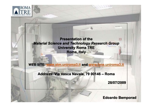
Presentation of the<br />
Material Science and Technology Research Group<br />
University <strong>Roma</strong> <strong>TRE</strong><br />
<strong>Roma</strong>, Italy<br />
WEB SITE: www.stm.uniroma3.it and www.lime.uniroma3.it<br />
Address: Via Vasca Navale, 79 00146 – <strong>Roma</strong><br />
28/07/2009<br />
Edoardo Bemporad
WHERE IS THE UNIVERSITY “ROMA <strong>TRE</strong>”?<br />
2
ROMA <strong>TRE</strong>, SOME NUMBERS…<br />
www.uniroma3.it<br />
Founded in 1992.<br />
One of the 4 State University in<br />
Rome (9 in total).<br />
175.000 m 2 .<br />
More than 40.000 000 students<br />
(4.100 enrolled in Engineering)<br />
More than 700 Researchers e s and<br />
Professors.<br />
Faculty of Engineering:<br />
• Civilil<br />
• Computer Science<br />
• Electronic<br />
• Mechanical<br />
Materials Science and Technology<br />
research <strong>group</strong> (<strong>STM</strong> Group)<br />
3
MORE INFO..<br />
www.stm.uniroma3.it<br />
4<br />
4
MORE INFO..<br />
www.lime.uniroma3.it<br />
5<br />
5
OUTLINE<br />
Research Group <strong>presentation</strong><br />
• People and research Partners<br />
• Vision<br />
• Facilities<br />
Ongoing g research<br />
Research topics on surface mechanical<br />
measurements and microstructure concerns,<br />
future activities<br />
6
<strong>STM</strong> GROUP:<br />
2 Full professors<br />
1 researcher<br />
1 graduated technician<br />
mechanical engineer, Graduate Technician<br />
3 Ph.D Students<br />
materials science and engineering<br />
2 fellowships<br />
(1 Sr + 1Jr mechanical Engineers)<br />
1 staff<br />
3 undergraduate (average) doing their<br />
“Laurea” thesis<br />
7
PRINCIPAL RESEARCH PARTNERS (CUSTOMERS)<br />
<br />
<br />
<br />
<br />
Private Firms<br />
INFN – Laboratori Nazionali di<br />
Legnaro (Pd)<br />
ENEA Casaccia dipartimento<br />
Materiali (RM)<br />
Centro Sviluppo Materiali (RM)<br />
<br />
<br />
National Research Council<br />
(CNR)<br />
• Department of Molecular<br />
Design<br />
• Others involved in surface<br />
engineering<br />
University of Oxford<br />
Department of Engineering<br />
Science<br />
<br />
National Universities<br />
• Ancona<br />
• Brescia<br />
• Cagliari<br />
• Firenze<br />
• Milano<br />
• Modena<br />
• Napoli<br />
• <strong>Roma</strong> 1<br />
• <strong>Roma</strong> 2<br />
• Torino<br />
<br />
<br />
<br />
<br />
<br />
SIO and Technische Universität<br />
Chemnitz (Germany)<br />
Central University of<br />
Venezuela, School of Metallurgy<br />
and Materials Science<br />
Lille University Laboratoire de<br />
Mécanique<br />
University of Rosario<br />
(Argentina)<br />
Karlsruhe Forschungszentrum<br />
(Germany)<br />
8
<strong>STM</strong> GROUP: VISION<br />
Product/process<br />
optimization<br />
Characterization<br />
methods: tuning<br />
and/or specific<br />
development<br />
Improving of<br />
understanding<br />
capabilities<br />
Needs of<br />
phenomena<br />
explanation<br />
Development<br />
Advanced d use<br />
Routine use<br />
9
<strong>STM</strong> GROUP: RESEARCH STRATEGY<br />
Development of methodologies for materials<br />
processing optimisation by the use of the paradigm:<br />
Coated system Design<br />
nanostructure-microstructure–properties-performancesperformances<br />
Optimization and failure analysis<br />
Multiscale and multidisciplinary<br />
approach.<br />
Modelling and simulating in<br />
service behaviour, reliability<br />
and degradation modalities (materials oriented)<br />
10
WE KEEP ATTENTION TO:<br />
<br />
Workflow concerns<br />
• Privacy<br />
• Timing<br />
• Cost control<br />
• Reporting<br />
Data and samples handling concerns<br />
• Redoundancy<br />
• Affordability<br />
• Accessibility<br />
• Privacy<br />
• Report standardization (Corporate Identity)<br />
11
<strong>STM</strong> FACILITIES: 3 LABORATORIES + 1 (IN DEV.)<br />
1. LIME, Electron Microscopy lab<br />
• Optical / Electronic / Stylus / (Ion Probing)<br />
2. MatEDP, Materials Modeling lab<br />
• 10 PC stations, Thermocalc, ANSYS, ABAQUS,<br />
Elastica, EFS,…<br />
3. MaTec, Materials Technology lab<br />
• Mechanical characterization (Hardness, Microhardness,<br />
Abrasive Wear, Scratch), Salt Spray,<br />
Fretting<br />
4. CoaTec, Coating technologies Lab<br />
• Work in progress, coating facility to be acquired<br />
within year 2010 (enhanced PVD process)<br />
12
<strong>STM</strong> FACILITIES: CONNECTION LAYOUT<br />
Building one<br />
Internet<br />
Offices 2° floor<br />
WAN <strong>Roma</strong> <strong>TRE</strong><br />
EXTRANET<br />
HTTPS - Certificates<br />
MatEDP 1° floor<br />
Building two<br />
PHILIPS XL 30 LaB 6<br />
ANALYTICAL<br />
CoaTec base floor<br />
Optic Fibers<br />
LIME<br />
and<br />
MaTec<br />
PHILIPS CM 120 TEM<br />
EDX (EDAX 134 Ev)<br />
13
LIME AND MATEC, FROM THE VERY BEGINNING…!<br />
14
LIME AND MATEC: LAB LAYOUT<br />
Digital Optical<br />
Microscopy,<br />
Macro-Micro-Nano<br />
Indenters<br />
Macro-nano-scratch<br />
Classroom<br />
Prep line<br />
SEM<br />
TEM<br />
Prep room<br />
AFM<br />
Dualbeam<br />
15
LIME LAB: SEM (FEI)<br />
• 30 Kv LaB 6 filament<br />
• Secondary electrons<br />
• Backscattered electrons<br />
• EDS to B, line & maps<br />
• Cathode luminescence<br />
• Specimen Current<br />
16
LIME LAB: TEM (FEI)<br />
• 120kV LaB 6 filament<br />
• Double tilt<br />
• EDS to B, point & line<br />
• nanoprobe<br />
17
LIME LAB: AFMS (1 NT-MDT + 1 DI)<br />
•50x50x5 microns range<br />
•All modes (contact, non<br />
contact, lateral force,…)<br />
18
LIME LAB: DUALBEAM (FEI) HELIOS 600 NANOLAB<br />
early 2008<br />
-Omnprobe<br />
-GIS(4 gases)<br />
-STEM<br />
- EDS (Oxford)<br />
19<br />
19
DUALBEAM (FEI)<br />
SEM Column: spatial resolution<br />
0,76 nm @ 15 kV<br />
FIB Column: spatial resolution<br />
5 nm @ 30 kV<br />
20
PRINCIPAL FIB MODES:<br />
Deposition<br />
Imaging<br />
Milling<br />
21
LIME LAB: DUALBEAM (FEI)<br />
0,76 nm res<br />
22
LIME LAB: DUALBEAM (FEI)<br />
23
LIME LAB: NON-CONTACT PROFILOMETRY (TALYSURF<br />
CCI L LITE) )<br />
24
LIME-LAB SELF-PRODUCING OF STANDARD<br />
SAMPLES FOR INSTRUMENTS CALIBRATION<br />
Calibration of the profilometer<br />
25
LIME-LAB SELF-PRODUCING OF STANDARD<br />
SAMPLES FOR INSTRUMENTS CALIBRATION<br />
Calibration of the profilometer<br />
26
MATEC LAB: HARDNESS TESTERS<br />
Vickers<br />
Knoop<br />
27
MATEC LAB: SCRATCH TESTER<br />
Depth profiling<br />
Applied force feedback controlled<br />
Acoustic emission sensor<br />
Friction force measurement<br />
28
MATEC LAB: NANOINDENTATION –NANOSCRATCH<br />
Agilent Nano Indenter<br />
G200<br />
End of 2007<br />
29<br />
29
MATEC LAB: SALT SPRAY 1M 3 CHAMBER<br />
30<br />
30
MATEC LAB: CONTACT ANGLE AND WETTABILITY<br />
Uni en 828 and A<strong>STM</strong> D5725 - 99<br />
31
SEMI-AUTOMATED INSTRUMENT FOR CONTACT ANGLE MEASUREMENT AND<br />
SURFACE FREE ENERGY MODELS<br />
SFE models:<br />
1. Zisman<br />
2. Neumann<br />
3. Girifalco<br />
4. Fowkes<br />
5. Owens-Wendt<br />
6. Van Oss-Chaudhury-Good<br />
Light source,<br />
polarized filter,<br />
screen diffuser<br />
Sample holder(three<br />
axes movement)<br />
12X objectives<br />
Digital Camera to<br />
acquire images on a<br />
PC<br />
32
IMPROVEMENT AND OPTIMIZATION OF THE SURFACE FREE<br />
ENERGY OF POLYMERIC SUBSTRATES BY FLAME <strong>TRE</strong>ATMENT<br />
Process parameters observed:<br />
1. Total flow rate;<br />
2. Oxygen/propane ratio;<br />
3. Distance sample-tip nozzle;<br />
4. Frequency of sample pass on<br />
flame;<br />
5. Total time treatment.<br />
Some results obtained through<br />
DOE Technique<br />
33
MACRO-SCALE INSTRUMENTED SPHERICAL<br />
INDENTATION<br />
Prototipal ti instrument t for macroscale<br />
spherical indentation<br />
The stress-strain curve is obtained by<br />
least-square fitting of exp data with a<br />
FEM-modelled database of L-h curves<br />
34
MATEC LAB: WEAR TEST<br />
Wear test device (prototype)<br />
Dynamic measurement of wear and friction coefficient at<br />
the sub-micron scale<br />
001<br />
002 003 004 005<br />
Campione 004<br />
-502<br />
60<br />
-502,5<br />
50<br />
[um]<br />
Affondamento [<br />
-503<br />
-503,5<br />
-504<br />
-504,5<br />
Affondamento<br />
Carico<br />
R 2 =0,98<br />
40<br />
30<br />
20<br />
10<br />
0<br />
Carico [g]<br />
-505<br />
-10<br />
0 10 20 30 40 50 60 70 80 90 100 110 120 130 140 150<br />
Tempo [s]<br />
35
OUTLINE<br />
Research Group <strong>presentation</strong><br />
• People and research Partners<br />
• Vision<br />
• Facilities<br />
Ongoing g research<br />
Research topics on surface mechanical<br />
measurements and microstructure concerns,<br />
future activities<br />
36
ONGOING RESEARCH<br />
<br />
<br />
<br />
<br />
<br />
<br />
<br />
<br />
<br />
<br />
<br />
Residual stress: FIB & Digital Imaging Correlation, FIB & nanoindentation<br />
Analysis of wear mechanisms by FIB-SEM techniques<br />
The use of statistical nanoindentation techniques for the mechanical<br />
characterization of cement pastes<br />
FIB-based failure analysis and nano-mechanical characterization of MEMS<br />
structures<br />
Scratch testing of thin coatings: failure modes mapping by FIB-SEM<br />
morphological analysis<br />
Improvement and optimization of the surface energy of polymeric substrates<br />
by Flame treatment<br />
Development of a semi-automated instrument for surface energy<br />
measurement<br />
Microstructural and mechanical characterization of cellular ceramics obtained<br />
by gel casting<br />
Instrumented spherical indentation at the<br />
macro-scale for the assessment the stress-strain curves of metals<br />
Use of nano-silica for preventing expansive alkali-silica reaction in concrete<br />
Microstructural and mechanical characterization of sputtered niobium thin<br />
films for accelerating cavity applications<br />
37
COATINGS: FAILURE MODES STUDY<br />
38
SCRATCH TESTING OF THIN COATINGS: FAILURE MODES<br />
MAPPING BY FIB-SEM MORPHOLOGICAL ANALYSIS<br />
Wedge spallation<br />
39
SCRATCH TESTING OF THIN COATINGS: FAILURE MODES MAPPING<br />
BY FIB-SEM MORPHOLOGICAL ANALYSIS<br />
Duplex Ti/TiN multilayer on WC-CO Planar:<br />
L c3: 38,5 N<br />
• FIB section in correspondence of the first<br />
chipping with substrate appearence<br />
40
SCRATCH TEST<br />
Duplex Ti/TiN<br />
multilayer on WC-<br />
CO Planar;<br />
• Adhesion can be worsen by an<br />
high h compressive residual<br />
stress that is additive with the<br />
scratch stress in front of the<br />
contact area<br />
41
ANALYSIS OF WEAR MECHANISMS BY FIB-SEM<br />
TECHNIQUES<br />
FIB analysis of mechanisms and crosssectional<br />
microstructural evolution during inservice<br />
wear of a Stellite 6B cobalt-based<br />
alloy subjected to sliding contact conditions<br />
FIB section of the worn surface FIB section outside the worn surface 42
RESONANT CAVITIES FOR PARTICLE ACCELERATORS<br />
Bulk Niobium<br />
Niobium Coated (PVD)<br />
Copper cavity<br />
Very low Surface<br />
electrical<br />
resistance<br />
(∼nΩ a 1,8 K)<br />
Lower costs<br />
Higher thermal stability<br />
But…<br />
Significantly lower<br />
superconducting properties<br />
– WHY??<br />
43
COATINGS ON COPPER SUBSTRATE<br />
BIASED<br />
(e-f) and<br />
UNBIASED<br />
(CERN, g-h)<br />
type coatings<br />
on QUARTZ<br />
substrate<br />
44
NANOINDENTATION ON NB THINFILMS<br />
Sample (mN<br />
N)<br />
Load On<br />
1<br />
0,9<br />
08<br />
0,8<br />
0,7<br />
0,6<br />
0,5<br />
0,4<br />
0,3<br />
0,2<br />
0,1<br />
0<br />
0 50 100<br />
Displacement Into Surface (nm)<br />
Niobium film load-depth<br />
curve<br />
Load On Sample (mN)<br />
p<br />
0,03<br />
0,025<br />
0,02<br />
0,015<br />
0,01<br />
0,005<br />
0<br />
0 5 10 15 20 25<br />
Displacement Into Surface (nm)<br />
Niobium film: Detail of a<br />
load-depth curve<br />
Indenter pop-in systematically observed<br />
at depth ~ 10 nm<br />
45
TEM ANALYSIS OF THE OXIDE LAYER<br />
TEM sample preparation p by<br />
FIB lamella thinning<br />
The control of surface oxide layer can be<br />
very important in determining the<br />
functional performances of Nb coatings<br />
for superconducting applications<br />
46
NANOINDENTATION ON MS-PVD NB THIN FILMS<br />
500 nm<br />
Partial recrystallization<br />
during<br />
plastic deformation;<br />
Relative sliding of<br />
columnar grain<br />
Measurement of<br />
indenter contact<br />
radius<br />
Direct measurement of<br />
piling-up<br />
Evaluation of the effects<br />
of roughness on contact<br />
area<br />
Analysis of deformation<br />
mechanisms<br />
47
MICRO INDENTATION ON MS-PVD NB THINFILMS<br />
Biased MS E = 88,95 GPa<br />
unbiased MS E = 54,33 GPa<br />
48
NANOINDENTATION ON S<strong>TRE</strong>SS RELIEVED PILLARS<br />
Compressive<br />
stress in the<br />
coating<br />
49
RESULTS –S<strong>TRE</strong>SS CALCULATIONS<br />
a) Pillar – stress free b) Halfspace stressed coating – as measured<br />
c) Modelled: Halfspace coating + RS<br />
50
CONTACT AREAS AND NANO STRUCTURAL EFFECTS<br />
Pillar – no RS<br />
Halfspace coating<br />
51
RESIDUAL S<strong>TRE</strong>ESS BY<br />
FIB-DIC TECHNIQUES<br />
Z=0 vs each step<br />
<br />
<br />
<br />
<br />
Incremental Milling;<br />
Steps of 200 nm<br />
The pillar size d is<br />
equal to the coating<br />
thickness<br />
The maximum milling<br />
depth is equal to the<br />
coating thickness<br />
(3.8 µm)<br />
52
EXPERIMENTAL DATA<br />
53
USE OF STATISTICAL NANOINDENTATION TECHNIQUES FOR<br />
THE MECHANICAL CHARACTERIZATION OF CEMENT PASTES<br />
54
FIB-BASED FAILURE ANALYSIS AND NANO-MECHANICAL<br />
CHARACTERIZATION OF MEMS STRUCTURES<br />
calculation of the stiffness of MEMS membrane by the use of a wedge<br />
indenter – spring stiffness taken into account<br />
55
MULTISCALE MECHANICAL CHARACTERIZATION OF<br />
POROUS CERAMICS<br />
FIB section and analysis<br />
of sub-superficial<br />
porosity<br />
56
MULTISCALE MECHANICAL CHARACTERIZATION OF<br />
POROUS CERAMICS<br />
⎛<br />
σ ⎜ max<br />
= σ<br />
0<br />
1+<br />
2<br />
⎝<br />
a ⎞<br />
⎟<br />
ρ<br />
⎠<br />
Radius of curvature<br />
at the apex of this<br />
pore is 55 nm!<br />
High stress<br />
intensification at<br />
crack tip<br />
Vertical drop in<br />
Hardness/Modulus<br />
is due to brittle<br />
failure of subsurface<br />
porosity!<br />
57
USE OF NANO-SILICA FOR PREVENTING EXPANSIVE ALKALI-<br />
SILICA REACTION IN CONCRETE<br />
• NS – SEM-FEG and TEM<br />
Analysis<br />
No tendency to particle<br />
agglomeration<br />
<br />
Particle dimension<br />
10.5±2.3 nm<br />
• BET specific surface area<br />
345 m 2 /g<br />
TEM-BF 50000x<br />
TEM-BF 380000x<br />
58
USE OF NANO-SILICA FOR PREVENTING EXPANSIVE<br />
ALKALI-SILICA REACTION IN CONCRETE<br />
Nano-Silica<br />
RILEM AAR-4 Expansion test at 60 °C - 90 days<br />
RILEM AAR-4 Expansion test at 60 °C - 150 days<br />
025 0,25<br />
0,25<br />
0,2<br />
Aggregate A<br />
Aggregate B<br />
0,2<br />
Aggregate A<br />
Aggregate B<br />
0,15<br />
0,15<br />
0,1<br />
Expansion limit at 60 °C<br />
0,1 Expansion limit at 60 °C<br />
0,05<br />
0,05<br />
0<br />
0 0,2 0,4 0,8 2 5<br />
Nano-silica content (wt %)<br />
0<br />
0 0,2 0,4 0,8 2 5<br />
Nano-silica content (wt %)<br />
Ultima ate test expansion E90 (% l/l)<br />
0,25<br />
0,2<br />
0,15<br />
0,1<br />
0,05<br />
0<br />
Berra et Al. Expansion test at 150 °C - 21 days<br />
Aggregate A<br />
Aggregate B<br />
• Aggregate A:<br />
Expansion<br />
limit a 150 °C<br />
D eff = 0,56% at 60°C - 0,03%<br />
0 0,2 0,4 0,8 2 5<br />
Nano-silica content (wt %)<br />
<br />
D eff = 0,58% at 150 °C - 0,12%<br />
The addition of NS is effective in<br />
reducine the expansion of<br />
concrete<br />
59
OUTLINE<br />
Research Group <strong>presentation</strong><br />
• People and research Partners<br />
• Vision<br />
• Facilities<br />
Ongoing g research<br />
Research topics on surface mechanical<br />
measurements and microstructure concerns,<br />
future activities<br />
60
FUTURE RESEARCH ACTIVITIES<br />
FIB + Nanoindents<br />
• Improving pillar and half space modeling: not only<br />
the edges of the pillars must be taken into into<br />
account, but also the layered character of the<br />
sample. Taking into account properly the real<br />
layered structure and reevaluate the real Young's<br />
modulus of the coating can be crucial.<br />
• A concept for direct access to the contact area<br />
without guess work and / or tip calibration even in<br />
the Angstrom scale (we give support to Norbert<br />
Schwarzer work, Saxonian Institute of Surface<br />
Mechanics)<br />
61
FUTURE RESEARCH ACTIVITIES<br />
FIB + DIC<br />
• Improving stress profiling method, which no other<br />
method can in a site specific way by the use of a<br />
more efficient correlation algorithms<br />
• Extension of the method to different coated<br />
systems, with different elastic and plastic behaviour<br />
at different scale values (i.e. soft materials or<br />
foams)<br />
62
RELATED PUBLICATIONS: 2008-2009<br />
1. A. KORSUNSKY, M. SEBASTIANI, E. BEMPORAD,<br />
Residual Stress Evaluation at the Micrometre Scale: FIB Ring-Drilling and Digital Image<br />
Correlation Analysis,<br />
Acta Materialia, submitted;<br />
2. A. KORSUNSKY, M. SEBASTIANI, E. BEMPORAD,<br />
FIB Ring-Drilling illi For Residual Stress Evaluation,<br />
Materials Letters, in press, doi:10.1016/j.matlet.2009.06.020 ;<br />
3. C. Bartuli, J.M. Tulliani, E. Bemporad, J. Tirillò, G. Pulci, M. Sebastiani, Mechanical properties of<br />
cellular ceramics obtained by gel casting: characterization and modeling, Journal of the<br />
European Ceramic Society, in press, doi:10.1016/j.jeurceramsoc.2009.04.035<br />
4. Jean - Marc Tulliani, Cecilia Bartuli, Edoardo d Bemporad, Valentina Naglieri, Marco Sebastiani,<br />
Preparation and mechanical characterization of dense and porous zirconia produced by gel<br />
casting with gelatin as a gelling agent, Ceramics International 35 (2009) 2481–2491<br />
5. RIZZO A, SIGNORE MA, TAPFER L, PISCOPIELLO E, CAPPELLO A, BEMPORAD E, EBASTIANI M,<br />
Graded selective coatings based on zirconium and titanium oxynitride, Journal of physics d:<br />
apllied physics, 42, 2009, 1-10<br />
10<br />
6. Bemporad E. and Carassiti F. and Sebastiani M. and Lanza G. and Palmieri V. and Padamsee H.,<br />
Superconducting and microstructural studies on sputtered niobium thin films for accelerating<br />
cavity applications, SUPERCONDUCTOR SCIENCE AND TECHNOLOGY, 21, 2008<br />
7. E. BEMPORAD, M. SEBASTIANI, F. CARASSITI, Tribological studies on PVD/HVOF duplex<br />
coatings on Ti6Al4V substrate t , Surface & Coatings Technology 203 (2008) 566–571571<br />
8. CARASSITI F. and SEBASTIANI M. and MANGIALARDI T. and PAOLINI A.E. and BERRA M. , USE<br />
OF NANO-SILICA FOR PREVENTING EXPANSIVE ALKALI-SILICA REACTION IN CONCRETE,<br />
proceedings of the ICAAR 2008 – 13th International Conference on Alkali-Aggregate<br />
Reaction in Concrete<br />
9. BEMPORAD E. , SEBASTIANI M., CASADEI F., CARASSITI F., Modelling, production and<br />
characterisation of duplex coatings (HVOF and PVD) on Ti–6Al–4V substrate for specific<br />
mechanical applications, Surface & Coatings Technology 201 (2007) 7652–7662<br />
10. E. Bemporad, M. Sebastiani, F. Carassiti, R. Valle, F. Casadei, Development of a duplex coating<br />
procedure (HVOF and PVD) on TI-6AL-4V substrate for automotive applications, Ceramic<br />
Engineering and Science Proceedings 28 (3), pp. 145-158158 ISBN 978-0-470-24679-5<br />
64
e.bemporad@stm.uniroma3.it<br />
marco.sebastiani@stm.uniroma3.it<br />
i@ t i it<br />
65