Design Of Digital Circuits - Dharmsinh Desai University
Design Of Digital Circuits - Dharmsinh Desai University Design Of Digital Circuits - Dharmsinh Desai University
Design Of Digital Circuits Lab Manual 1 AIM: Implement half adder and full adder circuits Sample experiment 2 TOOLS/APPARATUS: IC 7486, IC 7432, IC 7408, IC 7400, Power supply, Connecting wires, Multimeter etc. 3 STANDARD PROCEDURES: 3.1 Analyzing the Problem: To implement half and full adder we require X-OR gates, AND gates, OR Gate. Pin Diagrams of these gates are as below. Pin Diagrams of Basic gates ICs used in experiment: XOR Gate(IC 7486) AND Gate(IC 7408) OR Gate(IC 7432) Truth Tables of Basic gates used in experiment: Department of Information Technology, Faculty of Technology, D. D. University, Nadiad. 1
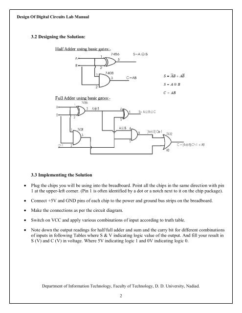
Design Of Digital Circuits Lab Manual 3.2 Designing the Solution: 3.3 Implementing the Solution Plug the chips you will be using into the breadboard. Point all the chips in the same direction with pin 1 at the upper-left corner. (Pin 1 is often identified by a dot or a notch next to it on the chip package). Connect +5V and GND pins of each chip to the power and ground bus strips on the breadboard. Make the connections as per the circuit diagram. Switch on VCC and apply various combinations of input according to truth table. Note down the output readings for half/full adder and sum and the carry bit for different combinations of inputs in following Tables where S & V indicating logic value of the output. And fill your result in S (V) and C (V) in voltage. Where 5V indicating logic 1 and 0V indicating logic 0. Department of Information Technology, Faculty of Technology, D. D. University, Nadiad. 2
- Page 1 and 2: Laboratory Manual For Design of Dig
- Page 3: List of Figures: Fig: 1.1 Power Sup
- Page 7 and 8: Design Of Digital Circuits Lab Manu
- Page 9 and 10: Design Of Digital Circuits Lab Manu
- Page 11 and 12: Design Of Digital Circuits Lab Manu
- Page 13 and 14: Design Of Digital Circuits Lab Manu
- Page 15 and 16: Design Of Digital Circuits Lab Manu
- Page 17 and 18: Design Of Digital Circuits Lab Manu
- Page 19 and 20: Design Of Digital Circuits Lab Manu
- Page 21 and 22: Design Of Digital Circuits Lab Manu
- Page 23 and 24: Design Of Digital Circuits Lab Manu
- Page 25 and 26: Design Of Digital Circuits Lab Manu
- Page 27 and 28: Design Of Digital Circuits Lab Manu
- Page 29 and 30: Design Of Digital Circuits Lab Manu
- Page 31 and 32: Design Of Digital Circuits Lab Manu
- Page 33 and 34: Design Of Digital Circuits Lab Manu
- Page 35 and 36: Design Of Digital Circuits Lab Manu
- Page 37 and 38: Design Of Digital Circuits Lab Manu
- Page 39 and 40: Design Of Digital Circuits Lab Manu
- Page 41 and 42: Design Of Digital Circuits Lab Manu
- Page 43 and 44: Design Of Digital Circuits Lab Manu
- Page 45 and 46: Design Of Digital Circuits Lab Manu
- Page 47 and 48: Design Of Digital Circuits Lab Manu
- Page 49 and 50: Design Of Digital Circuits Lab Manu
- Page 51 and 52: Design Of Digital Circuits Lab Manu
- Page 53 and 54: Design Of Digital Circuits Lab Manu
<strong>Design</strong> <strong>Of</strong> <strong>Digital</strong> <strong>Circuits</strong> Lab Manual<br />
3.2 <strong>Design</strong>ing the Solution:<br />
3.3 Implementing the Solution<br />
<br />
<br />
<br />
<br />
<br />
Plug the chips you will be using into the breadboard. Point all the chips in the same direction with pin<br />
1 at the upper-left corner. (Pin 1 is often identified by a dot or a notch next to it on the chip package).<br />
Connect +5V and GND pins of each chip to the power and ground bus strips on the breadboard.<br />
Make the connections as per the circuit diagram.<br />
Switch on VCC and apply various combinations of input according to truth table.<br />
Note down the output readings for half/full adder and sum and the carry bit for different combinations<br />
of inputs in following Tables where S & V indicating logic value of the output. And fill your result in<br />
S (V) and C (V) in voltage. Where 5V indicating logic 1 and 0V indicating logic 0.<br />
Department of Information Technology, Faculty of Technology, D. D. <strong>University</strong>, Nadiad.<br />
2


