

NX3008PBK 30 V, 230 mA P-channel Trench MOSFET
NX3008PBK 30 V, 230 mA P-channel Trench MOSFET
NX3008PBK 30 V, 230 mA P-channel Trench MOSFET

Create successful ePaper yourself
Turn your PDF publications into a flip-book with our unique Google optimized e-Paper software.
NXP Semiconductors<br />
<strong>NX<strong>30</strong>08PBK</strong><br />
<strong>30</strong> V, 2<strong>30</strong> <strong>mA</strong> P-<strong>channel</strong> <strong>Trench</strong> <strong>MOSFET</strong><br />
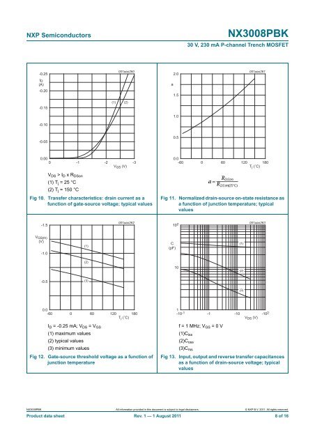
-0.25<br />
001aao260<br />
2.0<br />
001aao261<br />
I D<br />
(A)<br />
a<br />
-0.20<br />
1.5<br />
-0.15<br />
(1)<br />
(2)<br />
1.0<br />
-0.10<br />
-0.05<br />
0.5<br />
0.00<br />
0 -1<br />
-2<br />
-3<br />
V GS (V)<br />
V DS > I D x R DSon<br />
(1) T j = 25 °C<br />
(2) T j = 150 °C<br />
Fig 10. Transfer characteristics: drain current as a<br />
function of gate-source voltage; typical values<br />
0.0<br />
-60 0 60 120 180<br />
T j (˚C)<br />
Fig 11. Normalized drain-source on-state resistance as<br />
a function of junction temperature; typical<br />
values<br />
-1.5<br />
001aao262<br />
10 2<br />
001aao263<br />
V GS(th)<br />
(V)<br />
-1.0<br />
(1)<br />
C<br />
(pF)<br />
(1)<br />
(2)<br />
10<br />
(2)<br />
-0.5<br />
(3)<br />
(3)<br />
0.0<br />
-60 0 60 120 180<br />
T j (˚C)<br />
I D = -0.25 <strong>mA</strong>; V DS = V GS<br />
(1) maximum values<br />
(2) typical values<br />
(3) minimum values<br />
Fig 12. Gate-source threshold voltage as a function of<br />
junction temperature<br />
1<br />
-10 -1 -1<br />
-10<br />
-10 2<br />
V DS (V)<br />
f = 1 MHz; V GS = 0 V<br />
(1)C iss<br />
(2)C oss<br />
(3)C rss<br />
Fig 13. Input, output and reverse transfer capacitances<br />
as a function of drain-source voltage; typical<br />
values<br />
<strong>NX<strong>30</strong>08PBK</strong> All information provided in this document is subject to legal disclaimers. © NXP B.V. 2011. All rights reserved.<br />
Product data sheet Rev. 1 — 1 August 2011 8 of 16


