

Data Sheet - Microchip
Data Sheet - Microchip
Data Sheet - Microchip

Create successful ePaper yourself
Turn your PDF publications into a flip-book with our unique Google optimized e-Paper software.
PIC24FJXXXDA1/DA2/GB2/GA3<br />
PIC24FJXXXDA1/DA2/GB2/GA3 Families Flash<br />
Programming Specification<br />
1.0 DEVICE OVERVIEW<br />
This document defines the programming specification<br />
for the PIC24FJXXXDA1/DA2/GB2/GA3 families of<br />
16-bit microcontrollers (MCUs). This programming<br />
specification is required only for those developing programming<br />
support for the PIC24FJXXXDA1/DA2/GB2/<br />
GA3 families. Customers using only one of these<br />
devices should use development tools that already<br />
provide support for device programming.<br />
This specification includes programming specifications<br />
for the following devices:<br />
• PIC24FJ128DA106<br />
• PIC24FJ128DA110<br />
• PIC24FJ128DA206<br />
• PIC24FJ128DA210<br />
• PIC24FJ128GB206<br />
• PIC24FJ128GB210<br />
• PIC24FJ64GA310<br />
• PIC24FJ64GA308<br />
• PIC24FJ64GA306<br />
• PIC24FJ256DA106<br />
• PIC24FJ256DA110<br />
• PIC24FJ256DA206<br />
• PIC24FJ256DA210<br />
• PIC24FJ256GB206<br />
• PIC24FJ256GB210<br />
• PIC24FJ128GA310<br />
• PIC24FJ128GA308<br />
• PIC24FJ128GA306<br />
Topics covered include:<br />
1.0 Device Overview ................................................. 1<br />
2.0 Programming Overview of the PIC24FJXXXDA1/<br />
DA2/GB2/GA3 Families ..................................... 1<br />
3.0 Device Programming – ICSP ............................ 14<br />
4.0 Device Programming – Enhanced ICSP ........... 29<br />
5.0 The Programming Executive ............................. 42<br />
6.0 Device Details ................................................... 54<br />
7.0 AC/DC Characteristics and Timing<br />
Requirements .................................................. 56<br />
2.0 PROGRAMMING OVERVIEW<br />
OF THE PIC24FJXXXDA1/DA2/<br />
GB2/GA3 FAMILIES<br />
There are two methods of programming the<br />
PIC24FJXXXDA1/DA2/GB2/GA3 families of devices<br />
discussed in this programming specification. They are:<br />
• In-Circuit Serial Programming (ICSP)<br />
• Enhanced In-Circuit Serial Programming<br />
(Enhanced ICSP)<br />
The ICSP programming method is the most direct<br />
method to program the device; however, it is also the<br />
slower of the two methods. It provides native, low-level<br />
programming capability to erase, program and verify<br />
the chip.<br />
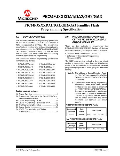
Note 1: The address of Special Function Register,<br />
‘TBLPAG’, has changed from 0x32 to<br />
0x54 in the PIC24FJXXXDA1/DA2/GB2/<br />
GA3 family.<br />
2: In the cases where legacy programming<br />
specification code from other device<br />
families is used as a basis to implement<br />
the PIC24FJXXXDA1/DA2/GB2/GA3 family<br />
programming specification, special care<br />
must be taken to ensure all references to<br />
‘TBLPAG’ in any existing code are updated<br />
with the correct opcode hex data for the<br />
mnemonic and operands (as shown<br />
below).<br />
PIC24FJXXXDA1/DA2/GB2/GA3 Family<br />
Command<br />
(Binary)<br />
<strong>Data</strong><br />
(Hex)<br />
Description<br />
0000 8802A0 MOV W0, TBLPAG<br />
Non PIC24FJXXXDA1/DA2/GB2/GA3 Family<br />
Command<br />
(Binary)<br />
<strong>Data</strong><br />
(Hex)<br />
Description<br />
0000 880190 MOV W0, TBLPAG<br />
2010 <strong>Microchip</strong> Technology Inc. DS39970B-page 1
PIC24FJXXXDA1/DA2/GB2/GA3<br />
The Enhanced In-Circuit Serial Programming<br />
(Enhanced ICSP) protocol uses a faster method that<br />
takes advantage of the programming executive, as<br />
illustrated in Figure 2-1. The programming executive<br />
provides all the necessary functionality to erase, program<br />
and verify the chip through a small command set.<br />
The command set allows the programmer to program<br />
the PIC24FJXXXDA1/DA2/GB2/GA3 MCUs without<br />
having to deal with the low-level programming<br />
protocols of the chip.<br />
FIGURE 2-1:<br />
Programmer<br />
PROGRAMMING SYSTEM<br />
OVERVIEW FOR<br />
ENHANCED ICSP<br />
This specification is divided into major sections that<br />
describe the programming methods independently.<br />
Section 3.0 “Device Programming – ICSP” describes<br />
the In-Circuit Serial Programming method. Section 4.0<br />
“Device Programming – Enhanced ICSP” describes<br />
the Run-Time Self-Programming (RTSP) method.<br />
2.1 Power Requirements<br />
PIC24FJXXXDA1/DA2/GB2/GA3<br />
Programming<br />
Executive<br />
On-Chip Memory<br />
All PIC24FJXXXDA1/DA2/GB2/GA3 devices power<br />
their core digital logic at a nominal 1.8V. To simplify system<br />
design, all devices in the PIC24FJXXXDA1/DA2/<br />
GB2/GA3 families incorporate an on-chip regulator that<br />
allows the device to run its core logic from VDD. For the<br />
PIC24F128GA310 family, the regulator is always<br />
enabled, so there is no ENVREG pin on the device.<br />
The regulator provides power to the core from the other<br />
VDD pins. A low-ESR capacitor (such as ceramic or tantalum)<br />
must be connected to the VCAP pin (see Table 2-1<br />
and Figure 2-2). This helps to maintain the stability of the<br />
regulator. The specifications for core voltage and capacitance<br />
are listed in Section 7.0 “AC/DC Characteristics<br />
and Timing Requirements”.<br />
2.2 Program Memory Write/Erase<br />
Requirements<br />
The Flash program memory on PIC24FJXXXDA1/DA2/<br />
GB2/GA3 devices has a specific write/erase requirement<br />
that must be adhered to for proper device<br />
operation. Any given word in memory must not be<br />
written more than twice before erasing the page where it<br />
is located. Thus, the easiest way to conform to this rule<br />
is to write all of the data in a programming block within<br />
one write cycle. The programming methods specified in<br />
this specification comply with this requirement.<br />
Note:<br />
2.3 Pin Diagrams<br />
Figure 2-4 through Figure 2-10 provide the pin diagrams<br />
for the PIC24FJXXXDA1/DA2/GB2/GA3 families. The<br />
pins that are required for programming are listed in<br />
Table 2-1 and are indicated in bold text in the figures.<br />
Refer to the appropriate device data sheet for complete<br />
pin descriptions.<br />
2.3.1 PGECx AND PGEDx PIN PAIRS<br />
All of the devices in the PIC24FJXXXDA1/DA2/GB2/<br />
GA3 families have three separate pairs of programming<br />
pins, labelled as PGEC1/PGED1, PGEC2/PGED2<br />
and PGEC3/PGED3. Any one of these pin pairs may be<br />
used for device programming by either ICSP or<br />
Enhanced ICSP. Unlike voltage supply and ground<br />
pins, it is not necessary to connect all three pin pairs to<br />
program the device. However, the programming<br />
method must use both pins of the same pair.<br />
FIGURE 2-2:<br />
FIGURE 2-3:<br />
Writing to a location multiple times without<br />
erasing is not recommended.<br />
CONNECTIONS FOR THE<br />
ON-CHIP REGULATOR<br />
Regulator Enabled (ENVREG tied to VDD):<br />
3.3V<br />
PIC24FJXXXDA1/DA2/GB2<br />
CEFC<br />
(10 F typ)<br />
VDD<br />
ENVREG<br />
VCAP<br />
VSS<br />
CONNECTIONS FOR THE<br />
VBAT PIN<br />
Regulator Enabled (VBAT tied to VDD or a Battery):<br />
3.3V<br />
PIC24FJXXXGA3<br />
VDD<br />
VBAT<br />
CEFC<br />
(10 F typ)<br />
VCAP<br />
VSS<br />
DS39970B-page 2<br />
2010 <strong>Microchip</strong> Technology Inc.
PIC24FJXXXDA1/DA2/GB2/GA3<br />
TABLE 2-1:<br />
Pin Name<br />
PIN DESCRIPTIONS (DURING PROGRAMMING)<br />
During Programming<br />
Pin Name Pin Type Pin Description<br />
MCLR MCLR P Programming Enable<br />
ENVREG (2) ENVREG (2) I Enable for On-Chip Voltage Regulator<br />
VDD and AVDD (1) VDD P Power Supply<br />
VSS and AVSS (1) VSS P Ground<br />
VCAP VCAP P On-Chip Voltage Regulator Output to the Core<br />
PGECx PGECx I Programming Pin Pairs 1, 2 and 3: Serial Clock<br />
PGEDx PGEDX I/O Programming Pin Pairs 1, 2 and 3: Serial <strong>Data</strong><br />
Legend: I = Input, O = Output, P = Power<br />
Note 1: All power supply and ground pins must be connected, including analog supplies (AVDD) and ground<br />
(AVSS).<br />
2: There is no ENVREG pin in the GA310 family. The regulator is always enabled and the ENVREG pin is<br />
replaced by the VBAT pin. It is recommended to connect the VBAT pin to the battery or VDD during<br />
programming.<br />
FIGURE 2-4:<br />
PIN DIAGRAM (64-PIN TQFP)<br />
RE4<br />
RE3<br />
RE2<br />
RE1<br />
RF0<br />
ENVREG<br />
VCAP<br />
RD7<br />
RD6<br />
RD5<br />
RD4<br />
RD3<br />
RD2<br />
RD1<br />
RE5<br />
RE6<br />
RE7<br />
RG6<br />
RG7<br />
RG8<br />
MCLR<br />
RG9<br />
VDD<br />
PGEC3/AN5/C1INA/VBUSON/RP18/CN7/RB5<br />
PGED3/AN4/C1INB/USBOEN/RP28/CN6/RB4<br />
RB3<br />
RB2<br />
PGEC1/AN1/RP1/VREF-/CN3/RB1<br />
PGED1/AN0/VREF+/RP0/ CN2/RB0<br />
1<br />
2<br />
3<br />
4<br />
5<br />
6<br />
7<br />
8<br />
9<br />
10<br />
11<br />
12<br />
13<br />
14<br />
15<br />
16<br />
PIC24FJXXXDAX06<br />
17<br />
18<br />
19<br />
20<br />
21<br />
22<br />
23<br />
24<br />
25<br />
26<br />
27<br />
28<br />
29<br />
30<br />
31<br />
32<br />
48<br />
47<br />
46<br />
45<br />
44<br />
43<br />
42<br />
41<br />
40<br />
39<br />
RC14<br />
RC13<br />
RD0<br />
RD11<br />
RD10<br />
RD9<br />
RD8<br />
VSS<br />
RC15<br />
RC12<br />
VDD<br />
RG2<br />
RG3<br />
RF6<br />
RF2<br />
RF3<br />
PGEC2/AN6/RP6/CN24/RB6<br />
PGED2/AN7/RP7/RCV/CN25/RB7<br />
AVDD<br />
RB8<br />
RB9<br />
RB10<br />
RB11<br />
VDD<br />
RB12<br />
RB13<br />
RB14<br />
RB15<br />
RF4<br />
RF5<br />
RE0<br />
RF1<br />
VSS<br />
VSS<br />
63<br />
62<br />
61<br />
60<br />
59<br />
58<br />
57<br />
56<br />
55<br />
54<br />
53<br />
52<br />
51<br />
50<br />
49<br />
38<br />
37<br />
36<br />
35<br />
34<br />
33<br />
AVSS<br />
64<br />
2010 <strong>Microchip</strong> Technology Inc. DS39970B-page 3
PIC24FJXXXDA1/DA2/GB2/GA3<br />
DS39970B-page 4<br />
2010 <strong>Microchip</strong> Technology Inc.<br />
FIGURE 2-5:<br />
PIN DIAGRAM (64-PIN)<br />
2<br />
3<br />
4<br />
5<br />
6<br />
7<br />
8<br />
9<br />
10<br />
11<br />
12<br />
13<br />
14<br />
15<br />
16<br />
48<br />
47<br />
22<br />
44<br />
24<br />
25<br />
26<br />
27<br />
28<br />
29<br />
30<br />
31<br />
32<br />
PIC24FJXXXGA306<br />
1<br />
46<br />
45<br />
23<br />
43<br />
42<br />
41<br />
40<br />
39<br />
RD6<br />
RD5<br />
RD4<br />
RD3<br />
RD2<br />
RD1<br />
RE4<br />
RE3<br />
RE2<br />
RE1<br />
RF0<br />
VCAP<br />
RC13<br />
RD0<br />
RD10<br />
RD9<br />
RD8<br />
RD11<br />
RC15<br />
RC12<br />
VDD<br />
RG2<br />
RF6<br />
RF2<br />
RF3<br />
RG3<br />
RC14<br />
AVDD<br />
RB8<br />
RB9<br />
RB10<br />
RB11<br />
VDD<br />
PGEC2/AN6/RP6/LCDBIAS3/CN24/RB6<br />
PGED2/AN7/RP7/CN25/RB7<br />
RF5<br />
RF4<br />
RE5<br />
RE6<br />
RE7<br />
RG6<br />
VDD<br />
PGEC3/AN5/C1INA/RP18/SEG2/CN7/RB5<br />
PGED3/AN4/C1INB/RP28/SEG3/CN6/RB4<br />
RB3<br />
RB2<br />
RG7<br />
RG8<br />
PGEC1/CVREF-/AN1/RP1/SEG6//CN3/RB1<br />
PGED1/CVREF+/AN0/RP0/SEG7/PMA6/CN2/RB0<br />
RG9<br />
MCLR<br />
RB12<br />
RB13<br />
RB14<br />
RB15<br />
RE0<br />
RF1<br />
RD7<br />
VSS<br />
VSS<br />
VSS<br />
VBAT<br />
63<br />
62<br />
61<br />
59<br />
60<br />
58<br />
57<br />
56<br />
54<br />
55<br />
53<br />
52<br />
51<br />
49<br />
50<br />
38<br />
37<br />
34<br />
36<br />
35<br />
33<br />
17<br />
19<br />
20<br />
21<br />
18<br />
AVSS<br />
64
2010 <strong>Microchip</strong> Technology Inc. DS39970B-page 5<br />
PIC24FJXXXDA1/DA2/GB2/GA3<br />
FIGURE 2-6:<br />
PIN DIAGRAM (64-PIN TQFP)<br />
2<br />
3<br />
4<br />
5<br />
6<br />
7<br />
8<br />
9<br />
10<br />
11<br />
12<br />
13<br />
14<br />
15<br />
16<br />
48<br />
47<br />
22<br />
44<br />
24<br />
25<br />
26<br />
27<br />
28<br />
29<br />
30<br />
31<br />
32<br />
PIC24FJXXXGB206<br />
1<br />
46<br />
45<br />
23<br />
43<br />
42<br />
41<br />
40<br />
39<br />
RD6<br />
RD5<br />
RD4<br />
RD3<br />
RD2<br />
RD1<br />
RE4<br />
RE3<br />
RE2<br />
RE1<br />
RF0<br />
VCAP<br />
RC13<br />
RD0<br />
RD9<br />
RD8<br />
RC15<br />
RC12<br />
VDD<br />
D+/RG2<br />
VUSB<br />
VBUS<br />
RF3<br />
D-/RG3<br />
AVDD<br />
RB8<br />
RB9<br />
RB10<br />
RB11<br />
VDD<br />
PGEC2/AN6/RP6/CN24/RB6<br />
PGED2/AN7/RP7/RCV/CN25/RB7<br />
RF5<br />
RF4<br />
RE5<br />
RE6<br />
RE7<br />
RG6<br />
VDD<br />
PGEC3/AN5/RP18/VBUSON/C1INA/CN7/RB5<br />
PGED3/AN4/RP28/USBOEN/C1INB/CN6/RB4<br />
RB3<br />
RB2<br />
RG7<br />
RG8<br />
PGEC1/AN1/RP1/VREF-/CN3/RB1<br />
PGED1/AN0/RP0/VREF+/<br />
RG9<br />
MCLR<br />
RB12<br />
RB13<br />
RB14<br />
RB15<br />
RE0<br />
RF1<br />
RD7<br />
VSS<br />
VSS<br />
VSS<br />
ENVREG<br />
63<br />
62<br />
61<br />
59<br />
60<br />
58<br />
57<br />
56<br />
54<br />
55<br />
53<br />
52<br />
51<br />
49<br />
50<br />
38<br />
37<br />
34<br />
36<br />
35<br />
33<br />
17<br />
19<br />
20<br />
21<br />
18<br />
AVSS<br />
64<br />
RC14<br />
CN2/RB0<br />
RD10<br />
RD11
PIC24FJXXXDA1/DA2/GB2/GA3<br />
DS39970B-page 6<br />
2010 <strong>Microchip</strong> Technology Inc.<br />
FIGURE 2-7:<br />
PIN DIAGRAM (80-PIN TQFP)<br />
80<br />
79<br />
78<br />
20<br />
2<br />
3<br />
4<br />
5<br />
6<br />
7<br />
8<br />
9<br />
10<br />
11<br />
12<br />
13<br />
14<br />
15<br />
16<br />
60<br />
59<br />
26<br />
56<br />
40<br />
39<br />
28<br />
29<br />
30<br />
31<br />
32<br />
33<br />
34<br />
35<br />
36<br />
37<br />
38<br />
PIC24FJXXXGA308<br />
17<br />
18<br />
19<br />
1<br />
76<br />
77<br />
58<br />
57<br />
27<br />
55<br />
54<br />
53<br />
52<br />
51<br />
RD5<br />
RD4<br />
RD13<br />
RD12<br />
RD3<br />
RD2<br />
RD1<br />
RE2<br />
RE1<br />
RE0<br />
RG0<br />
RE4<br />
RE3<br />
RF0<br />
VCAP<br />
RC13<br />
RD0<br />
RD10<br />
RD9<br />
RD8<br />
RD11<br />
RA15<br />
RA14<br />
RC15<br />
RC12<br />
VDD<br />
RG2<br />
RF6<br />
RF7<br />
RP15<br />
RG3<br />
RF2<br />
RF3<br />
RC14<br />
RA10<br />
RA9<br />
AVDD<br />
RB8<br />
RB9<br />
RB10<br />
RB11<br />
VDD<br />
RD14<br />
RD15<br />
PGEC2/AN6/RP6/LCDBIAS3/CN24/RB6<br />
PGED2/AN7/RP7/CN25/RB7<br />
RF5<br />
RF4<br />
RE5<br />
RE6<br />
RE7<br />
RC1<br />
RC3<br />
RG6<br />
VDD<br />
RE8<br />
RE9<br />
RB3<br />
RB2<br />
RG7<br />
RG8<br />
PGEC1/CVREF-/AN1/RP1/SEG6<br />
PGED1/CVREF+/AN0/RP0/SEG7<br />
RG9<br />
MCLR<br />
RB12<br />
RB13<br />
RB14<br />
RB15<br />
RG1<br />
RF1<br />
RD7<br />
RD6<br />
VSS<br />
VSS<br />
VSS<br />
VBAT<br />
75<br />
74<br />
73<br />
71<br />
72<br />
70<br />
69<br />
68<br />
66<br />
67<br />
65<br />
64<br />
63<br />
61<br />
62<br />
50<br />
49<br />
46<br />
48<br />
47<br />
45<br />
44<br />
43<br />
42<br />
41<br />
21<br />
23<br />
24<br />
25<br />
22<br />
AVSS<br />
PGEC3/AN5/C1INA/RP18/SEG2/CN7/RB5<br />
PGED3/AN4/C1INB/RP28/SEG3/CN6/RB4
2010 <strong>Microchip</strong> Technology Inc. DS39970B-page 7<br />
PIC24FJXXXDA1/DA2/GB2/GA3<br />
FIGURE 2-8:<br />
PIN DIAGRAM (100-PIN TQFP)<br />
92<br />
94<br />
93<br />
91<br />
90<br />
89<br />
88<br />
87<br />
86<br />
85<br />
84<br />
83<br />
82<br />
81<br />
80<br />
79<br />
78<br />
20<br />
2<br />
3<br />
4<br />
5<br />
6<br />
7<br />
8<br />
9<br />
10<br />
11<br />
12<br />
13<br />
14<br />
15<br />
16<br />
65<br />
64<br />
63<br />
62<br />
61<br />
60<br />
59<br />
26<br />
56<br />
45<br />
44<br />
43<br />
42<br />
41<br />
40<br />
39<br />
28<br />
29<br />
30<br />
31<br />
32<br />
33<br />
34<br />
35<br />
36<br />
37<br />
38<br />
PIC24XJXXXDAX10<br />
17<br />
18<br />
19<br />
21<br />
22<br />
95<br />
1<br />
76<br />
77<br />
72<br />
71<br />
70<br />
69<br />
68<br />
67<br />
66<br />
75<br />
74<br />
73<br />
58<br />
57<br />
24<br />
23<br />
25<br />
96<br />
98<br />
97<br />
99<br />
27<br />
46<br />
47<br />
48<br />
49<br />
50<br />
55<br />
54<br />
53<br />
52<br />
51<br />
100<br />
RD5<br />
RD4<br />
RD13<br />
RD12<br />
RD3<br />
RD2<br />
RD1<br />
RA7<br />
RA6<br />
RE2<br />
RG13<br />
RG12<br />
RG14<br />
RE1<br />
RE0<br />
RG0<br />
RE4<br />
RE3<br />
RF0<br />
VCAP<br />
RC13<br />
RD0<br />
RD9<br />
RD8<br />
RA15<br />
RA14<br />
RC15<br />
RC12<br />
VDD<br />
RG2<br />
RF6<br />
RF7<br />
RF8<br />
RG3<br />
RF2<br />
RF3<br />
VSS<br />
RA10<br />
RA9<br />
AVDD<br />
AVSS<br />
RB8<br />
RB9<br />
RB10<br />
RB11<br />
VDD<br />
RF12<br />
RF13<br />
VSS<br />
VDD<br />
RD15<br />
RD14<br />
PGEC2/AN6/RP6/CN24/RB6<br />
PGED2/AN7/RP7/RCV/GPWR/CN25/RB7<br />
RF5<br />
RF4<br />
RE5<br />
RE6<br />
RE7<br />
RC1<br />
RC2<br />
RC3<br />
RC4<br />
RG6<br />
VDD<br />
RA0<br />
RE8<br />
RE9<br />
RB3<br />
RB2<br />
RG7<br />
RG8<br />
PGEC1/AN1/RP1/CN3/RB1<br />
PGED1/AN0/RP0CN2/RB0<br />
RG15<br />
VDD<br />
RG9<br />
MCLR<br />
RB12<br />
RB13<br />
RB14<br />
RB15<br />
RG1<br />
RF1<br />
RD7<br />
RD6<br />
RA5<br />
RA3<br />
RA2<br />
VSS<br />
VSS<br />
VSS<br />
ENVREG<br />
RA4<br />
RA1<br />
RC14<br />
RD10<br />
RD11<br />
PGEC3/AN5/RP18/VBUSON/C1INA/CN7/RB5<br />
PGED3/AN4/C1INB/USBOEN// RP28/GD4/CN6/RB4
PIC24FJXXXDA1/DA2/GB2/GA3<br />
DS39970B-page 8<br />
2010 <strong>Microchip</strong> Technology Inc.<br />
FIGURE 2-9:<br />
PIN DIAGRAM (100-PIN TQFP)<br />
92<br />
94<br />
93<br />
91<br />
90<br />
89<br />
88<br />
87<br />
86<br />
85<br />
84<br />
83<br />
82<br />
81<br />
80<br />
79<br />
78<br />
20<br />
2<br />
3<br />
4<br />
5<br />
6<br />
7<br />
8<br />
9<br />
10<br />
11<br />
12<br />
13<br />
14<br />
15<br />
16<br />
65<br />
64<br />
63<br />
62<br />
61<br />
60<br />
59<br />
26<br />
56<br />
45<br />
44<br />
43<br />
42<br />
41<br />
40<br />
39<br />
28<br />
29<br />
30<br />
31<br />
32<br />
33<br />
34<br />
35<br />
36<br />
37<br />
38<br />
PIC24FJXXXGA310<br />
17<br />
18<br />
19<br />
21<br />
22<br />
95<br />
1<br />
76<br />
77<br />
72<br />
71<br />
70<br />
69<br />
68<br />
67<br />
66<br />
75<br />
74<br />
73<br />
58<br />
57<br />
24<br />
23<br />
25<br />
96<br />
98<br />
97<br />
99<br />
27<br />
46<br />
47<br />
48<br />
49<br />
50<br />
55<br />
54<br />
53<br />
52<br />
51<br />
100<br />
RD5<br />
RD4<br />
RD13<br />
RD12<br />
RD3<br />
RD2<br />
RD1<br />
RA7<br />
RA6<br />
RE2<br />
RG13<br />
RG12<br />
RG14<br />
RE1<br />
RE0<br />
RG0<br />
RE4<br />
RE3<br />
RF0<br />
VCAP<br />
RC13<br />
RD0<br />
RD10<br />
RD9<br />
RD8<br />
RD11<br />
RA15<br />
RA14<br />
RC15<br />
RC12<br />
VDD<br />
RG2<br />
RF6<br />
RF7<br />
RF8<br />
RG3<br />
RF2<br />
RF3<br />
VSS<br />
RC14<br />
RA10<br />
RA9<br />
AVDD<br />
AVSS<br />
RB8<br />
RB9<br />
RB10<br />
RB11<br />
VDD<br />
RF12<br />
RF13<br />
VSS<br />
VDD<br />
RD15<br />
RD14<br />
PGEC2/AN6/RP6/LCDBIAS3/CN24/RB6<br />
PGED2/AN7/RP7/CN25/RB7<br />
RF5<br />
RF4<br />
RE5<br />
RE6<br />
RE7<br />
RC1<br />
RC2<br />
RC3<br />
RC4<br />
RG6<br />
VDD<br />
RA0<br />
RE8<br />
RE9<br />
PGC3/AN5/C1INA/RP18/SEG2/CN7/RB5<br />
RB3<br />
RB2<br />
RG7<br />
RG8<br />
PGEC1/CVREF-/AN1/RB1/SEG6<br />
PGED1/CVREF+/AN0/RB0/SEG7<br />
RG15<br />
VDD<br />
RG9<br />
MCLR<br />
RB12<br />
RB13<br />
RB14<br />
RB15<br />
RG1<br />
RF1<br />
RD7<br />
RD6<br />
RA5<br />
RA3<br />
RA2<br />
VSS<br />
VSS<br />
VSS<br />
VBAT<br />
RA4<br />
RA1<br />
PGD3/AN4/C1INB/RP28/SEG3/CN6/RB4
2010 <strong>Microchip</strong> Technology Inc. DS39970B-page 9<br />
PIC24FJXXXDA1/DA2/GB2/GA3<br />
FIGURE 2-10:<br />
PIN DIAGRAM (100-PIN TQFP)<br />
92<br />
94<br />
93<br />
91<br />
90<br />
89<br />
88<br />
87<br />
86<br />
85<br />
84<br />
83<br />
82<br />
81<br />
80<br />
79<br />
78<br />
20<br />
2<br />
3<br />
4<br />
5<br />
6<br />
7<br />
8<br />
9<br />
10<br />
11<br />
12<br />
13<br />
14<br />
15<br />
16<br />
65<br />
64<br />
63<br />
62<br />
61<br />
60<br />
59<br />
26<br />
56<br />
45<br />
44<br />
43<br />
42<br />
41<br />
40<br />
39<br />
28<br />
29<br />
30<br />
31<br />
32<br />
33<br />
34<br />
35<br />
36<br />
37<br />
38<br />
PIC24XJXXXGB210<br />
17<br />
18<br />
19<br />
21<br />
22<br />
95<br />
1<br />
76<br />
77<br />
72<br />
71<br />
70<br />
69<br />
68<br />
67<br />
66<br />
75<br />
74<br />
73<br />
58<br />
57<br />
24<br />
23<br />
25<br />
96<br />
98<br />
97<br />
99<br />
27<br />
46<br />
47<br />
48<br />
49<br />
50<br />
55<br />
54<br />
53<br />
52<br />
51<br />
100<br />
RD5<br />
RD4<br />
RD13<br />
RD12<br />
RD3<br />
RD2<br />
RD1<br />
RA7<br />
RA6<br />
RE2<br />
RG13<br />
RG12<br />
RG14<br />
RE1<br />
RE0<br />
RG0<br />
RE4<br />
RE3<br />
RF0<br />
VCAP<br />
RC13<br />
RD0<br />
RD9<br />
RD8<br />
RA15<br />
RA14<br />
RC15<br />
RC12<br />
VDD<br />
D+/RG2<br />
VUSB<br />
VBUS<br />
RF8<br />
D-/RG3<br />
RF2<br />
RF3<br />
VSS<br />
RA10<br />
RA9<br />
AVDD<br />
AVSS<br />
RB8<br />
RB9<br />
RB10<br />
RB11<br />
VDD<br />
RF12<br />
RF13<br />
VSS<br />
VDD<br />
RD15<br />
RD14<br />
PGEC2/AN6/RP6/CN24/RB6<br />
PGED2/AN7/RP7/RCV/CN25/RB7<br />
RF5<br />
RF4<br />
RE5<br />
RE6<br />
RE7<br />
RC1<br />
RC2<br />
RC3<br />
RC4<br />
RG6<br />
VDD<br />
RA0<br />
RE8<br />
RE9<br />
RB3<br />
RB2<br />
RG7<br />
RG8<br />
PGEC1/CVREF-/AVREF-/AN1/RP1/CN3/RB1<br />
PGED1/CVREF-/AVREF-/AN0/RP0/CN2/RB0<br />
RG15<br />
VDD<br />
RG9<br />
MCLR<br />
RB12<br />
RB13<br />
RB14<br />
RB15<br />
RG1<br />
RF1<br />
RD7<br />
RD6<br />
RA5<br />
RA3<br />
RA2<br />
VSS<br />
VSS<br />
VSS<br />
ENVREG<br />
RA4<br />
RA1<br />
RC14<br />
RD10<br />
RD11<br />
PGEC3/AN5/RP18/VBUSON/ C1INA/CN7/RB5<br />
PGED3/AN4/RP28/USBOEN/ C1INB/CN6/RB4
PIC24FJXXXDA1/DA2/GB2/GA3<br />
FIGURE 2-11:<br />
PIC24FJXXXDAX10 121-PIN BGA PINOUT DIAGRAM<br />
1 2 3 4 5 6 7 8 9 10 11<br />
A<br />
RE4 RE3 RG13 RE0 RG0 RF1 ENVREG N/C RD12 RD2 RD1<br />
B<br />
N/C RG15 RE2 RE1 RA7 RF0 VCAP RD5 RD3 VSS RC14<br />
C<br />
RE6 VDD RG12 RG14 RA6 N/C RD7 RD4 VDD RC13 RD11<br />
D<br />
RC1 RE7 RE5 VSS VSS N/C RD6 RD13 RD0 N/C RD10<br />
E<br />
RC4 RC3 RG6 RC2 VDD RG1 N/C RA15 RD8 RD9 RA14<br />
F<br />
MCLR RG8 RG9 RG7 VSS N/C N/C VDD RC12 VSS RC15<br />
G<br />
RE8 RE9 RA0 N/C VDD VSS VSS N/C RA5 RA3 RA4<br />
H<br />
PGEC3/ PGED3/ VSS VDD N/C VDD N/C RF7 VUSB D+/RG2 RA2<br />
RB5 GD4/RB4 PGED2/<br />
J<br />
RB3<br />
RB2<br />
RB7<br />
GPWR/<br />
AVDD RB11 RA1 RB12 N/C N/C RF8 D-/RG3<br />
K<br />
L<br />
PGEC1/ PGED1/ RA10 RB8 N/C RF12 RB14 VDD RD15 RF3 RF2<br />
RB1 RB0<br />
PGEC2/ RA9 AVSS RB9 RB10 RF13 RB13 RB15 RD14 RF4 RF5<br />
RB6<br />
FIGURE 2-12:<br />
PIC24FJXXXGBX10 121-PIN BGA PINOUT DIAGRAM<br />
1 2 3 4 5 6 7 8 9 10 11<br />
A<br />
RE4 RE3 RG13 RE0 RG0 RF1 ENVREG N/C RD12 RD2 GD1<br />
B<br />
N/C RG15 RE2 RE1 RA7 RF0 VCAP RD5 RD3 VSS RC14<br />
C<br />
RE6 VDD RG12 RG14 RA6 N/C RD7 RD4 VDD RC13 RD11<br />
D<br />
RC1 RE7 RE5 VSS VSS N/C RD6 RD13 RD0 N/C RD10<br />
E<br />
RC4 RC3 RG6 RC2 VDD RG1 N/C RA15 RD8 RD10 RA14<br />
F<br />
MCLR RG8 RG9 RG7 VSS N/C N/C VDD RC12 VSS RC15<br />
G<br />
RE8 RE9 RA0 N/C VDD VSS VSS N/C RA5 RA3 RA4<br />
H<br />
J<br />
PGEC3/ PGED3/ VSS VDD N/C VDD N/C RF7 VUSB D+/RG2 RA2<br />
RB5 RB4<br />
RB3 RB2 PGED2/ RB7 AVDD RB11 RA1 RB12 N/C N/C RF8 D-/RG3<br />
K<br />
L<br />
PGEC1/ PGED1/ RA10 RB8 N/C RF12 RB14 VDD RD15 RF3 RF2<br />
RB1 RB0<br />
PGEC2/ RA9 AVSS RB9 RB10 RF13 RB13 RB15 RD14 RF4 RF5<br />
RB6<br />
DS39970B-page 10<br />
2010 <strong>Microchip</strong> Technology Inc.
PIC24FJXXXDA1/DA2/GB2/GA3<br />
FIGURE 2-13:<br />
PIC24FJXXXGA310 121-PIN BGA PINOUT DIAGRAM<br />
1 2 3 4 5 6 7 8 9 10 11<br />
A<br />
RE4 RE3 RG13 RE0 RG0 RF1 VBAT N/C RD12 RD2 RD1<br />
B<br />
C<br />
N/C RG15 RE2 RE1 RA7 RF0 VCAP/ RD5 RD3 VSS RC14<br />
VDDCORE<br />
RE6 VDD RG12 RG14 RA6 N/C RD7 RD4 VSS RC13 RD11<br />
D<br />
RC1<br />
RE7 RE5 VSS N/C N/C RD6 RD13 RD0 N/C RD10<br />
E<br />
RC4 RC3 RG6 RC2 N/C RG1 N/C RA15 RD8 RD9 RA14<br />
F<br />
G<br />
MCLR RG8 RG9 RG7 VSS N/C N/C VDD OSCI/ VSS OSCO/<br />
RC12<br />
RC15<br />
RE8 RE9 RA0 N/C VDD VSS VSS N/C RA5 RA3 RA4<br />
H<br />
RB5/<br />
PGEC3<br />
RB4/<br />
PGED3<br />
VSS VSS N/C VDD N/C RF7 RF6 RG2 RA2<br />
J<br />
RB3<br />
RB2<br />
RB7/<br />
PGED2<br />
AVDD RB11 RA1 RB12 N/C N/C RF8 RG3<br />
K<br />
L<br />
RB1/<br />
PGEC1<br />
RB6/<br />
PGEC2<br />
RB0/ RA10 RB8 N/C RF12 RB14 VDD RD15 RF3 RF2<br />
PGED1<br />
RA9 AVSS RB9 RB10 RF13 RB13 RB15 RD14 RF4 RF5<br />
2010 <strong>Microchip</strong> Technology Inc. DS39970B-page 11
PIC24FJXXXDA1/DA2/GB2/GA3<br />
2.4 Memory Map<br />
The program memory map extends from 000000h to<br />
FFFFFEh. Code storage is located at the base of the<br />
memory map and supports up to 87K instruction words<br />
(about 256 Kbytes). Table 2-2 provides the program<br />
memory size, and number of erase and program blocks<br />
present in each device variant. Each erase block, or<br />
page, contains 512 instructions, and each program<br />
block, or row, contains 64 instructions.<br />
Locations, 800000h through 8007FEh, are reserved for<br />
executive code memory. This region stores the<br />
programming executive and the debugging executive.<br />
The programming executive is used for device<br />
programming and the debugging executive is used for<br />
in-circuit debugging. This region of memory cannot be<br />
used to store user code.<br />
The last four implemented program memory locations<br />
are reserved for the Flash Configuration Words. The<br />
reserved addresses are provided in Table 2-2.<br />
Locations, FF0000h and FF0002h, are reserved for the<br />
Device ID registers. These bits can be used by the<br />
programmer to identify what device type is being<br />
programmed. They are described in Section 6.1<br />
“Device ID”. The Device ID registers read out<br />
normally, even after code protection is applied.<br />
Figure 2-14 displays the memory map for the<br />
PIC24FJXXXDA1/DA2/GB2/GA3 family variants.<br />
TABLE 2-2:<br />
Device<br />
CODE MEMORY SIZE AND FLASH CONFIGURATION WORD LOCATIONS FOR<br />
PIC24FJXXXDA1/DA2/GB2/GA3 DEVICES<br />
User Memory<br />
Address Limit<br />
(Instruction Words)<br />
Write<br />
Blocks<br />
Erase<br />
Blocks<br />
Configuration Word Addresses<br />
1 2 3 4<br />
PIC24FJ64GA3XX 00ABFEh (22K) 344 43 00ABFEh 00ABFCh 00ABFAh 00ABF8h<br />
PIC24FJ128DA1XX<br />
PIC24FJ128DA2XX 0157FEh (44K) 688 86 0157FEh 0157FCh 0157FAh 0157F8h<br />
PIC24FJ128GB2XX<br />
PIC24FJ128GA3XX<br />
PIC24FJ256DA1XX<br />
PIC24FJ256DA2XX 02ABFEh (87K) 1368 171 02ABFEh 02ABFCh 02ABFAh 02ABF8h<br />
PIC24FJ256GB2XX<br />
DS39970B-page 12<br />
2010 <strong>Microchip</strong> Technology Inc.
PIC24FJXXXDA1/DA2/GB2/GA3<br />
FIGURE 2-14:<br />
PROGRAM MEMORY MAP<br />
000000h<br />
User Flash<br />
Code Memory (1) 0XXX00h (1)<br />
Flash Configuration Words<br />
0XXXF7h (1)<br />
0XXXF8h (1)<br />
0XXXFEh (1)<br />
User Memory<br />
Space<br />
Reserved<br />
Executive Code Memory<br />
(1024 x 24-bit)<br />
7FFFFEh<br />
800000h<br />
8007FEh<br />
800800h<br />
Reserved Memory<br />
Configuration Memory<br />
Space<br />
Diagnostic and Calibration<br />
Words<br />
(8 x 24-bit)<br />
Reserved<br />
8008FEh<br />
800880h<br />
80088Eh<br />
Device ID<br />
(2 x 16-bit)<br />
Reserved<br />
FEFFFEh<br />
FF0000h<br />
FF0002h<br />
FF0004h<br />
FFFFFEh<br />
Note 1:<br />
The size and address boundaries for user Flash code memory are device dependent. See Table 2-2 for details.<br />
2010 <strong>Microchip</strong> Technology Inc. DS39970B-page 13
PIC24FJXXXDA1/DA2/GB2/GA3<br />
3.0 DEVICE PROGRAMMING – ICSP<br />
ICSP mode is a special programming protocol that<br />
allows you to read and write to the memory of<br />
PIC24FJXXXDA1/DA2/GB2/GA3 devices. The ICSP<br />
mode is the most direct method used to program the<br />
device; however, Enhanced ICSP is faster. ICSP mode<br />
also has the ability to read the contents of executive<br />
memory to determine if the programming executive is<br />
present. This capability is accomplished by applying<br />
control codes and instructions, serially to the device,<br />
using pins, PGECx and PGEDx.<br />
In ICSP mode, the system clock is taken from the<br />
PGECx pin, regardless of the device’s oscillator Configuration<br />
bits. All instructions are shifted serially into an<br />
internal buffer, then loaded into the Instruction Register<br />
(IR) and executed. No program fetching occurs from<br />
internal memory. Instructions are fed in 24 bits at a<br />
time. PGEDx is used to shift data in and PGECx is used<br />
as both the serial shift clock and the CPU execution<br />
clock.<br />
Note:<br />
During ICSP operation, the operating<br />
frequency of PGECx must not exceed<br />
10 MHz.<br />
3.1 Overview of the Programming<br />
Process<br />
See Figure 3-1 for high-level overview of the<br />
programming process. After entering ICSP mode, the<br />
first action is to Chip Erase the device. Next, the code<br />
memory is programmed, followed by the device<br />
Configuration registers. Code memory (including the<br />
Configuration registers) is then verified to ensure that<br />
programming was successful. Then, the code-protect<br />
Configuration bits are programmed, if required.<br />
3.2 ICSP Operation<br />
Upon entry into ICSP mode, the CPU is Idle. Execution<br />
of the CPU is governed by an internal state machine. A<br />
4-bit control code is clocked in using PGECx and<br />
PGEDx and this control code is used to command the<br />
CPU (see Table 3-1).<br />
The SIX control code is used to send instructions to the<br />
CPU for execution and the REGOUT control code is<br />
used to read data out of the device via the VISI register.<br />
TABLE 3-1:<br />
FIGURE 3-1:<br />
CPU CONTROL CODES IN<br />
ICSP MODE<br />
4-Bit<br />
Control Code Mnemonic Description<br />
0000 SIX Shift in 24-bit instruction<br />
and execute.<br />
0001 REGOUT Shift out the VISI<br />
(0784h) register.<br />
0010-1111 N/A Reserved.<br />
HIGH-LEVEL ICSP<br />
PROGRAMMING FLOW<br />
Start<br />
Enter ICSP<br />
Perform Chip<br />
Erase<br />
Program Memory<br />
Verify Program<br />
Program Configuration Bits<br />
Verify Configuration Bits<br />
Exit ICSP<br />
End<br />
DS39970B-page 14<br />
2010 <strong>Microchip</strong> Technology Inc.
PIC24FJXXXDA1/DA2/GB2/GA3<br />
3.2.1 SIX SERIAL INSTRUCTION<br />
EXECUTION<br />
The SIX control code allows execution of PIC24F family<br />
assembly instructions. When the SIX code is received,<br />
the CPU is suspended for 24 clock cycles, as the instruction<br />
is then clocked into the internal buffer. Once the<br />
instruction is shifted in, the state machine allows it to be<br />
executed over the next four PGECx clock cycles. While<br />
the received instruction is executed, the state machine<br />
simultaneously shifts in the next 4-bit command (see<br />
Figure 3-2).<br />
Coming out of Reset, the first 4-bit control code is<br />
always forced to SIX and a forced NOP instruction is<br />
executed by the CPU. Five additional PGECx clocks<br />
are needed on start-up, resulting in a 9-bit SIX<br />
command instead of the normal 4-bit SIX command.<br />
After the forced SIX is clocked in, ICSP operation<br />
resumes as normal. That is, the next 24 clock cycles<br />
load the first instruction word to the CPU.<br />
Note:<br />
To account for this forced NOP, all example<br />
code in this specification begins with a<br />
NOP to ensure that no data is lost.<br />
FIGURE 3-2:<br />
SIX SERIAL EXECUTION<br />
P1<br />
1 2 3 4 5 6 7 8 9 1 2 3 4 5 6 7 8 17 18 19 20 21 22 23 24 1 2 3 4<br />
PGECx<br />
P2<br />
0 0<br />
PGEDx<br />
P3<br />
0 0 0 0<br />
0 0 0<br />
P4<br />
P1A<br />
P1B<br />
LSB X X X X X X X X X X X X X X MSB<br />
P4A<br />
0 0 0 0<br />
Execute PC – 1,<br />
Fetch SIX<br />
Control Code<br />
Only for<br />
Program<br />
Memory Entry<br />
24-Bit Instruction Fetch<br />
PGEDx = Input<br />
Execute 24-Bit<br />
Instruction, Fetch<br />
Next Control Code<br />
3.2.1.1 Differences Between the Execution<br />
of SIX and Normal Instructions<br />
There are some important differences between<br />
executing instructions normally and using the SIX ICSP<br />
command. Therefore, the code examples in this specification<br />
may not match those for performing the same<br />
functions during normal device operation.<br />
During SIX ICSP operation:<br />
• Two-word instructions require two SIX operations<br />
to clock in all the necessary data.<br />
Examples of two-word instructions are GOTO and<br />
CALL.<br />
• Two-cycle instructions require two SIX operations.<br />
The first SIX operation shifts in the instruction and<br />
begins to execute it. The second SIX operation,<br />
which should shift in a NOP to avoid losing data,<br />
provides the CPU clocks required to finish<br />
executing the instruction.<br />
Examples of two-cycle instructions are Table Read<br />
and Table Write instructions.<br />
• The CPU does not automatically stall to account<br />
for pipeline changes.<br />
A CPU stall occurs when an instruction modifies a<br />
register that is used for indirect addressing by the<br />
following instruction.<br />
During normal device operation:<br />
• The CPU automatically will force a NOP while the new<br />
data is read. When using ICSP, there is no automatic<br />
stall, so any indirect references to a recently modified<br />
register should be preceded by a NOP.<br />
For example, the instructions, MOV #0x0,W0 and<br />
MOV [W0],W1, must have a NOP inserted among<br />
them.<br />
If a two-cycle instruction modifies a register that is<br />
used indirectly, it will require two NOPs: one to<br />
execute the second half of the instruction and the<br />
other to stall the CPU to correct the pipeline.<br />
Instructions, such as TBLWTL [W0++],[W1],<br />
should be followed by two NOPs.<br />
• The device Program Counter (PC) continues to<br />
automatically increment during ICSP instruction<br />
execution, even though the Flash memory is not<br />
being used.<br />
As a result, the PC may be incremented to point to<br />
invalid memory locations. Invalid memory spaces<br />
include unimplemented Flash addresses and the<br />
vector space (locations: 0x0 to 0x1FF).<br />
If the PC points to these locations, the device will<br />
reset, possibly interrupting the ICSP operation. To<br />
prevent this, instructions should be periodically<br />
executed to reset the PC to a safe space. The<br />
optimal method to accomplish this is to perform a<br />
GOTO 0x200.<br />
2010 <strong>Microchip</strong> Technology Inc. DS39970B-page 15
PIC24FJXXXDA1/DA2/GB2/GA3<br />
3.2.2 REGOUT SERIAL INSTRUCTION<br />
EXECUTION<br />
The REGOUT control code allows for data to be<br />
extracted from the device in ICSP mode. It is used to<br />
clock the contents of the VISI register, out of the device,<br />
over the PGEDx pin. After the REGOUT control code is<br />
received, the CPU is held Idle for 8 cycles. After these<br />
8 cycles, an additional 16 cycles are required to clock the<br />
data out (see Figure 3-3).<br />
The REGOUT code is unique because the PGEDx pin<br />
is an input when the control code is transmitted to the<br />
device. However, after the control code is processed,<br />
the PGEDx pin becomes an output as the VISI register<br />
is shifted out.<br />
Note 1: After the contents of VISI are shifted out,<br />
the PIC24FJXXXDA1/DA2/GB2/GA3<br />
devices maintain PGEDx as an output<br />
until the first rising edge of the next clock<br />
is received.<br />
2: <strong>Data</strong> changes on the falling edge and<br />
latches on the rising edge of PGECx. For<br />
all data transmissions, the Least<br />
Significant bit (LSb) is transmitted first.<br />
FIGURE 3-3:<br />
REGOUT SERIAL EXECUTION<br />
PGECx<br />
1 2 3 4 1 2 7 8<br />
P4<br />
P5<br />
1 2 3 4 5 6 11 12 13 14 15 16 1 2 3 4<br />
P4A<br />
PGEDx<br />
1<br />
0<br />
0 0<br />
LSb 1 2 3 4 ... 10 11 12 13 14 MSb 0 0 0 0<br />
Execute Previous Instruction, CPU Held in Idle Shift Out VISI Register<br />
Fetch REGOUT Control Code<br />
No Execution Takes Place,<br />
Fetch Next Control Code<br />
PGEDx = Input<br />
PGEDx = Output<br />
PGEDx = Input<br />
DS39970B-page 16<br />
2010 <strong>Microchip</strong> Technology Inc.
PIC24FJXXXDA1/DA2/GB2/GA3<br />
3.3 Entering ICSP Mode<br />
As displayed in Figure 3-4, entering ICSP Program/Verify<br />
mode requires three steps:<br />
1. MCLR is briefly driven high, then low.<br />
2. A 32-bit key sequence is clocked into PGEDx.<br />
3. MCLR is then driven high within a specified<br />
period and held.<br />
The programming voltage applied to MCLR is VIH,<br />
which is essentially VDD in the case of<br />
PIC24FJXXXDA1/DA2/GB2/GA3 devices. There is no<br />
minimum time requirement for holding at VIH. After VIH<br />
is removed, an interval of at least P18 must elapse<br />
before presenting the key sequence on PGEDx.<br />
The key sequence is a specific 32-bit pattern:<br />
‘0100 1101 0100 0011 0100 1000 0101 0001’<br />
(more easily remembered as 4D434851h in hexadecimal).<br />
The device will enter Program/Verify mode only<br />
if the sequence is valid. The Most Significant bit (MSb) of<br />
the most significant nibble must be shifted in first.<br />
Once the key sequence is complete, VIH must be<br />
applied to MCLR and held at that level for as long as<br />
Program/Verify mode is to be maintained. An interval of<br />
at least time, P19 and P7, must elapse before presenting<br />
data on PGEDx. Signals appearing on PGECx<br />
before P7 has elapsed will not be interpreted as valid.<br />
On successful entry, the program memory can be<br />
accessed and programmed in serial fashion. While in<br />
ICSP mode, all unused I/Os are placed in the<br />
high-impedance state.<br />
FIGURE 3-4:<br />
ENTERING ICSP MODE<br />
MCLR<br />
P6<br />
P14<br />
VIH<br />
VIH<br />
P19<br />
P7<br />
VDD<br />
PGEDx<br />
PGECx<br />
P18<br />
Program/Verify Entry Code = 4D434851h<br />
0 1 0 0 1 ... 0 0 0 1<br />
b31 b30 b29 b28 b27 b3 b2 b1 b0<br />
P1A<br />
P1B<br />
2010 <strong>Microchip</strong> Technology Inc. DS39970B-page 17
PIC24FJXXXDA1/DA2/GB2/GA3<br />
3.4 Flash Memory Programming in<br />
ICSP Mode<br />
3.4.1 PROGRAMMING OPERATIONS<br />
Flash memory write and erase operations are<br />
controlled by the NVMCON register. Programming is<br />
performed by setting NVMCON to select the type of<br />
erase operation (see Table 3-2) or write operation (see<br />
Table 3-3) and initiating the programming by setting the<br />
WR control bit (NVMCON).<br />
In ICSP mode, all programming operations are<br />
self-timed. There is an internal delay between the user<br />
setting the WR control bit and the automatic clearing of<br />
the WR control bit when the programming operation is<br />
complete. Refer to Section 7.0 “AC/DC Characteristics<br />
and Timing Requirements” for information about<br />
the delays associated with various programming<br />
operations.<br />
TABLE 3-2:<br />
NVMCON<br />
Value<br />
404Fh<br />
4042h<br />
TABLE 3-3:<br />
NVMCON<br />
Value<br />
4003h<br />
4001h<br />
NVMCON ERASE<br />
OPERATIONS<br />
Erase Operation<br />
Erase all code memory, executive<br />
memory and Configuration registers<br />
(does not erase Device ID registers).<br />
Erase a page of code memory or<br />
executive memory.<br />
NVMCON WRITE<br />
OPERATIONS<br />
Write Operation<br />
Write a single code memory word,<br />
Configuration Word or Executive Memory<br />
Word.<br />
Program 1 row (64 instruction words) of<br />
code memory or executive memory.<br />
3.5 Erasing Program Memory<br />
The procedure for erasing program memory (all of the<br />
code memory, data memory, executive memory and<br />
code-protect bits) consists of setting NVMCON to<br />
404Fh and executing the programming cycle.<br />
A Chip Erase can erase all of the user memory or all of<br />
both the user and configuration memory. A Table Write<br />
instruction should be executed prior to performing the<br />
Chip Erase to select which sections are erased.<br />
The Table Write instruction is executed:<br />
• If the TBLPAG register points to user space (is<br />
less than 0x80), the Chip Erase will erase only<br />
user memory and Flash Configuration Words.<br />
• If the TBLPAG register points to configuration<br />
space (is greater than or equal to 0x80), the Chip<br />
Erase is not allowed. The configuration space can<br />
be erased one page at a time.<br />
Note:<br />
Figure 3-5 displays the ICSP programming process for<br />
performing a Chip Erase. This process includes the<br />
ICSP command code, which must be transmitted (for<br />
each instruction), LSb first, using the PGECx and<br />
PGEDx pins (see Figure 3-2).<br />
Note:<br />
FIGURE 3-5:<br />
The Chip Erase is not allowed when the<br />
TBLPAG points to the configuration space<br />
to avoid the Diagnostic and Calibration<br />
Words from getting erased.<br />
Program memory must be erased before<br />
writing any data to program memory.<br />
CHIP ERASE FLOW<br />
Start<br />
Write 404Fh to NVMCON SFR<br />
Set the WR bit to Initiate Erase<br />
3.4.2 STARTING AND STOPPING A<br />
PROGRAMMING CYCLE<br />
The WR bit (NVMCON) is used to start an erase or<br />
write cycle. Setting the WR bit initiates the programming<br />
cycle.<br />
All erase and write cycles are self-timed. The WR bit<br />
should be polled to determine if the erase or write cycle<br />
has been completed. Starting a programming cycle is<br />
performed as follows:<br />
BSET NVMCON, #WR<br />
No<br />
Is WR bit<br />
cleared (‘0’)?<br />
Yes<br />
End<br />
DS39970B-page 18<br />
2010 <strong>Microchip</strong> Technology Inc.
PIC24FJXXXDA1/DA2/GB2/GA3<br />
TABLE 3-4:<br />
Command<br />
(Binary)<br />
Step 1:<br />
0000<br />
0000<br />
0000<br />
Step 2:<br />
0000<br />
0000<br />
Step 3:<br />
0000<br />
0000<br />
0000<br />
0000<br />
0000<br />
0000<br />
Step 4:<br />
0000<br />
0000<br />
0000<br />
Step 5:<br />
0000<br />
0000<br />
0000<br />
0000<br />
0000<br />
0001<br />
0000<br />
SERIAL INSTRUCTION EXECUTION FOR CHIP ERASE<br />
<strong>Data</strong><br />
(Hex)<br />
Exit the Reset vector.<br />
000000<br />
040200<br />
000000<br />
NOP<br />
GOTO<br />
NOP<br />
0x200<br />
Set the NVMCON to erase all program memory.<br />
2404FA<br />
883B0A<br />
MOV<br />
MOV<br />
#0x404F, W10<br />
W10, NVMCON<br />
Description<br />
Set TBLPAG and perform dummy Table Write to select what portions of memory are erased.<br />
2xxxx0<br />
8802A0<br />
200000<br />
BB0800<br />
000000<br />
000000<br />
Initiate the erase cycle.<br />
A8E761<br />
000000<br />
000000<br />
MOV<br />
MOV<br />
MOV<br />
TBLWTL<br />
NOP<br />
NOP<br />
BSET<br />
NOP<br />
NOP<br />
#, W0<br />
W0, TBLPAG<br />
#0x0000, W0<br />
W0,[W0]<br />
NVMCON, #WR<br />
Repeat this step to poll the WR bit (bit 15 of NVMCON) until it is cleared by the hardware.<br />
040200<br />
000000<br />
803B02<br />
883C22<br />
000000<br />
<br />
000000<br />
GOTO 0x200<br />
NOP<br />
MOV NVMCON, W2<br />
MOV W2, VISI<br />
NOP<br />
Clock out contents of the VISI register<br />
NOP<br />
2010 <strong>Microchip</strong> Technology Inc. DS39970B-page 19
PIC24FJXXXDA1/DA2/GB2/GA3<br />
3.6 Writing Code Memory<br />
The procedure for writing code memory is the same as<br />
that of writing the Configuration registers, except that<br />
64 instruction words are programmed at a time. To<br />
facilitate this operation, working registers, W0:W5, are<br />
used as temporary holding registers for the data to be<br />
programmed.<br />
Table 3-5 provides the ICSP programming details,<br />
including the serial pattern with the ICSP command<br />
code, which must be transmitted, LSb first, using the<br />
PGECx and PGEDx pins (see Figure 3-2).<br />
In Step 1, the Reset vector is exited. In Step 2, the<br />
NVMCON register is initialized for programming a full<br />
row of code memory. In Step 3, the 24-bit starting<br />
destination address for programming is loaded into the<br />
TBLPAG register and W7 register. (The upper byte of<br />
the starting destination address is stored in TBLPAG<br />
and the lower 16 bits of the destination address are<br />
stored in W7.)<br />
To minimize the programming time, a packed instruction<br />
format is used (see Figure 3-6).<br />
In Step 4, four packed instruction words are stored in<br />
working registers, W0:W5, using the MOV instruction<br />
and the Read Pointer, W6, is initialized. The contents of<br />
W0:W5 (holding the packed instruction word data) are<br />
displayed in Figure 3-6.<br />
In Step 5, eight TBLWT instructions are used to copy the<br />
data from W0:W5 to the write latches of code memory.<br />
Since code memory is programmed 64 instruction<br />
words at a time, Steps 4 and 5 are repeated 16 times to<br />
load all the write latches (Step 6).<br />
After the write latches are loaded, programming is<br />
initiated by writing to the NVMCON register in Steps 7<br />
and 8. In Step 9, the internal PC is reset to 200h. This<br />
is a precautionary measure to prevent the PC from<br />
incrementing into unimplemented memory when large<br />
devices are being programmed. Lastly, in Step 10,<br />
Steps 3-9 are repeated until all of the code memory is<br />
programmed.<br />
FIGURE 3-6:<br />
PACKED INSTRUCTION<br />
WORDS IN W0:W5<br />
15 8 7 0<br />
W0<br />
LSW0<br />
W1 MSB1 MSB0<br />
W2<br />
LSW1<br />
W3<br />
LSW2<br />
W4 MSB3 MSB2<br />
W5<br />
LSW3<br />
TABLE 3-5:<br />
Command<br />
(Binary)<br />
Step 1:<br />
0000<br />
0000<br />
0000<br />
Step 2:<br />
0000<br />
0000<br />
Step 3:<br />
0000<br />
0000<br />
0000<br />
Step 4:<br />
0000<br />
0000<br />
0000<br />
0000<br />
0000<br />
0000<br />
SERIAL INSTRUCTION EXECUTION FOR WRITING CODE MEMORY<br />
<strong>Data</strong><br />
(Hex)<br />
Exit the Reset vector.<br />
000000<br />
040200<br />
000000<br />
NOP<br />
GOTO 0x200<br />
NOP<br />
Set the NVMCON to program 64 instruction words.<br />
24001A<br />
883B0A<br />
MOV #0x4001, W10<br />
MOV W10, NVMCON<br />
Initialize the Write Pointer (W7) for TBLWT instruction.<br />
200xx0<br />
8802A0<br />
2xxxx7<br />
Description<br />
MOV #, W0<br />
MOV W0, TBLPAG<br />
MOV #, W7<br />
Load W0:W5 with the next 4 instruction words to program.<br />
2xxxx0<br />
2xxxx1<br />
2xxxx2<br />
2xxxx3<br />
2xxxx4<br />
2xxxx5<br />
MOV #, W0<br />
MOV #, W1<br />
MOV #, W2<br />
MOV #, W3<br />
MOV #, W4<br />
MOV #, W5<br />
DS39970B-page 20<br />
2010 <strong>Microchip</strong> Technology Inc.
PIC24FJXXXDA1/DA2/GB2/GA3<br />
TABLE 3-5:<br />
Command<br />
(Binary)<br />
Step 5: Set the Read Pointer (W6) and load the (next set of) write latches.<br />
0000 EB0300 CLR W6<br />
0000 000000 NOP<br />
0000<br />
0000<br />
0000<br />
0000<br />
0000<br />
0000<br />
0000<br />
0000<br />
0000<br />
0000<br />
0000<br />
0000<br />
0000<br />
0000<br />
0000<br />
0000<br />
0000<br />
0000<br />
0000<br />
0000<br />
0000<br />
0000<br />
0000<br />
0000<br />
BB0BB6<br />
000000<br />
000000<br />
BBDBB6<br />
000000<br />
000000<br />
BBEBB6<br />
000000<br />
000000<br />
BB1BB6<br />
000000<br />
000000<br />
BB0BB6<br />
000000<br />
000000<br />
BBDBB6<br />
000000<br />
000000<br />
BBEBB6<br />
000000<br />
000000<br />
BB1BB6<br />
000000<br />
000000<br />
TBLWTL [W6++], [W7]<br />
NOP<br />
NOP<br />
TBLWTH.B [W6++], [W7++]<br />
NOP<br />
NOP<br />
TBLWTH.B [W6++], [++W7]<br />
NOP<br />
NOP<br />
TBLWTL [W6++], [W7++]<br />
NOP<br />
NOP<br />
TBLWTL [W6++], [W7]<br />
NOP<br />
NOP<br />
TBLWTH.B [W6++], [W7++]<br />
NOP<br />
NOP<br />
TBLWTH.B [W6++], [++W7]<br />
NOP<br />
NOP<br />
TBLWTL [W6++], [W7++]<br />
NOP<br />
NOP<br />
Step 6: Repeat Steps 4 and 5, 16 times, to load the write latches for 64 instructions.<br />
Step 7: Initiate the write cycle.<br />
0000<br />
0000<br />
0000<br />
Step 8:<br />
0000<br />
0000<br />
0000<br />
0000<br />
0000<br />
0001<br />
0000<br />
Step 9:<br />
0000<br />
0000<br />
SERIAL INSTRUCTION EXECUTION FOR WRITING CODE MEMORY (CONTINUED)<br />
<strong>Data</strong><br />
(Hex)<br />
A8E761<br />
000000<br />
000000<br />
BSET NVMCON, #WR<br />
NOP<br />
NOP<br />
Repeat this step to poll the WR bit (bit 15 of NVMCON) until it is cleared by the hardware.<br />
040200<br />
000000<br />
803B02<br />
883C22<br />
000000<br />
<br />
000000<br />
Reset device internal PC.<br />
040200<br />
000000<br />
GOTO 0x200<br />
NOP<br />
MOV NVMCON, W2<br />
MOV W2, VISI<br />
NOP<br />
Clock out contents of the VISI register.<br />
NOP<br />
GOTO 0x200<br />
NOP<br />
Step 10: Repeat Steps 3 through 9 until all code memory is programmed.<br />
Description<br />
2010 <strong>Microchip</strong> Technology Inc. DS39970B-page 21
PIC24FJXXXDA1/DA2/GB2/GA3<br />
FIGURE 3-7:<br />
PROGRAM CODE MEMORY FLOW<br />
Start<br />
N = 1<br />
LoopCount = 0<br />
Configure<br />
Device for<br />
Writes<br />
N = N + 1<br />
Load 1 Instruction Word<br />
Write Buffer at <br />
No<br />
All<br />
instruction words<br />
written?<br />
N = 1<br />
LoopCount =<br />
LoopCount + 1<br />
Yes<br />
Start Write Sequence<br />
and Poll for WR bit<br />
to be Cleared<br />
No<br />
All<br />
locations<br />
done?<br />
End<br />
Yes<br />
DS39970B-page 22<br />
2010 <strong>Microchip</strong> Technology Inc.
PIC24FJXXXDA1/DA2/GB2/GA3<br />
3.7 Writing Configuration Words<br />
Device configuration for PIC24FJXXXDA1/DA2/GB2/<br />
GA3 devices is stored in Flash Configuration Words at<br />
the end of the user space program memory and in<br />
multiple register Configuration Words, located in the test<br />
space. These registers reflect values read at any Reset<br />
from program memory locations. The values for the Configuration<br />
Words for the default device configurations are<br />
listed in Table 3-6.<br />
The values can be changed only by programming the<br />
content of the corresponding Flash Configuration Word<br />
and resetting the device. The Reset forces an automatic<br />
reload of the Flash stored configuration values by<br />
sequencing through the dedicated Flash Configuration<br />
Words and transferring the data into the Configuration<br />
registers.<br />
For the PIC24FJXXXDA1/DA2/GB2/GA3 families, certain<br />
Configuration bits have default states that must<br />
always be maintained to ensure device functionality,<br />
regardless of the settings of other Configuration bits.<br />
To change the values of the Flash Configuration Word<br />
once it has been programmed, the device must be Chip<br />
Erased, as described in Section 3.5 “Erasing Program<br />
Memory” and reprogrammed to the desired value. It is<br />
not possible to program a ‘0’ to ‘1’; they may be<br />
programmed from a ‘1’ to ‘0’ to enable code protection.<br />
Table 3-7 provides the ICSP programming details for<br />
programming the Configuration Word locations, including<br />
the serial pattern with the ICSP command code,<br />
which must be transmitted, LSb first, using the PGECx<br />
and PGEDx pins (see Figure 3-2).<br />
In Step 1, the Reset vector is exited. In Step 2, the lower<br />
16 bits of the source address are stored in W7. In<br />
Step 3, the NVMCON register is initialized for programming<br />
of code memory. In Step 4, the upper byte of the<br />
24-bit starting source address for writing is loaded into<br />
the TBLPAG register.<br />
The TBLPAG register must be loaded with 00h for<br />
64 Kbytes, and 01h for 128 and 256 Kbytes devices.<br />
To verify the data by reading the Configuration Words<br />
after performing the write in order, the code protection<br />
bits initially should be programmed to a ‘1’ to ensure<br />
that the verification can be performed properly. After<br />
verification is finished, the code protection bit can be<br />
programmed to a ‘0’ by using a word write to the<br />
appropriate Configuration Word.<br />
TABLE 3-6:<br />
DEFAULT CONFIGURATION<br />
REGISTER VALUES<br />
Address Name Default Value<br />
Last Word CW1 7FFFh<br />
Last Word – 2 CW2 FFFFh<br />
Last Word – 4 CW3 FFFFh<br />
Last Word – 6 CW4 FFFFh<br />
2010 <strong>Microchip</strong> Technology Inc. DS39970B-page 23
PIC24FJXXXDA1/DA2/GB2/GA3<br />
TABLE 3-7:<br />
Command<br />
(Binary)<br />
Step 1:<br />
0000<br />
0000<br />
0000<br />
Step 2:<br />
SERIAL INSTRUCTION EXECUTION FOR WRITING CONFIGURATION REGISTERS<br />
<strong>Data</strong><br />
(Hex)<br />
Exit the Reset vector.<br />
000000<br />
040200<br />
000000<br />
NOP<br />
GOTO 0x200<br />
NOP<br />
Description<br />
Initialize the Write Pointer (W7) for the TBLWT instruction.<br />
0000 2xxxx7 MOV #, W7<br />
Step 3: Set the NVMCON register to program CW1.<br />
0000<br />
0000<br />
Step 4:<br />
0000<br />
0000<br />
24003A<br />
883B0A<br />
Initialize the TBLPAG register.<br />
200xx0<br />
8802A0<br />
MOV #0x4003, W10<br />
MOV W10, NVMCON<br />
MOV #, W0<br />
MOV W0, TBLPAG<br />
Step 5: Load the Configuration register data to W6.<br />
0000 2xxxx6 MOV #, W6<br />
Step 6: Write the Configuration register data to the write latch and decrement the Write Pointer.<br />
0000<br />
0000<br />
0000<br />
0000<br />
0000<br />
0000<br />
0000<br />
0000<br />
Step 7:<br />
0000<br />
0000<br />
0000<br />
Step 8:<br />
0000<br />
0000<br />
0000<br />
0000<br />
0000<br />
0001<br />
0000<br />
Step 9:<br />
0000<br />
0000<br />
200008<br />
000000<br />
BBCB88<br />
000000<br />
000000<br />
BB1386<br />
000000<br />
000000<br />
Initiate the write cycle.<br />
A8E761<br />
000000<br />
000000<br />
MOV #0x0000, W8<br />
NOP<br />
TBLWTH.B W8, [W7]<br />
NOP<br />
NOP<br />
TBLWTL.W W6, [W7--]<br />
NOP<br />
NOP<br />
BSET NVMCON, #WR<br />
NOP<br />
NOP<br />
Repeat this step to poll the WR bit (bit 15 of NVMCON) until it is cleared by the hardware.<br />
040200<br />
000000<br />
803B02<br />
883C22<br />
000000<br />
<br />
000000<br />
Reset device internal PC.<br />
GOTO 0x200<br />
NOP<br />
MOV NVMCON, W2<br />
MOV W2, VISI<br />
NOP<br />
Clock out contents of the VISI register.<br />
NOP<br />
040200 GOTO 0x200<br />
000000 NOP<br />
Step 10: Repeat Steps 5 through 9 to write Configuration Word 2 to Configuration Word 4.<br />
DS39970B-page 24<br />
2010 <strong>Microchip</strong> Technology Inc.
PIC24FJXXXDA1/DA2/GB2/GA3<br />
3.8 Reading Code Memory<br />
Reading from code memory is performed by executing<br />
a series of TBLRD instructions and clocking out the data<br />
using the REGOUT command.<br />
Table 3-8 provides the ICSP programming details for<br />
reading code memory. In Step 1, the Reset vector is<br />
exited. In Step 2, the Write Pointer, W7, is initialized. In<br />
Step 3, the 24-bit starting source address for reading is<br />
loaded into the TBLPAG register and W6 register. The<br />
upper byte of the starting source address is stored in<br />
TBLPAG and the lower 16 bits of the source address<br />
are stored in W6.<br />
To minimize the reading time, the packed instruction<br />
word format that was utilized for writing is also used for<br />
reading (see Figure 3-6). In Step 4, two instruction<br />
words are read from code memory and clocked out of<br />
the device, through the VISI register, using the<br />
REGOUT command. Step 4 is repeated until the<br />
desired amount of code memory is read.<br />
TABLE 3-8: SERIAL INSTRUCTION EXECUTION FOR READING CODE MEMORY<br />
Command <strong>Data</strong><br />
Description<br />
(Binary) (Hex)<br />
Step 1: Exit Reset vector.<br />
0000<br />
0000<br />
0000<br />
Step 2:<br />
0000<br />
0000<br />
Step 3:<br />
0000<br />
0000<br />
0000<br />
Step 4:<br />
0000<br />
0000<br />
0000<br />
0001<br />
0000<br />
0000<br />
0000<br />
0000<br />
0000<br />
0000<br />
0000<br />
0001<br />
0000<br />
0000<br />
0000<br />
0000<br />
0001<br />
0000<br />
Step 5:<br />
0000<br />
0000<br />
Step 6:<br />
000000<br />
040200<br />
000000<br />
NOP<br />
GOTO 0x200<br />
NOP<br />
Initialize the Write Pointer (W7) to point to the VISI register.<br />
207847<br />
000000<br />
MOV #VISI, W7<br />
NOP<br />
Initialize TBLPAG and the Read Pointer (W6) for TBLRD instruction.<br />
200xx0<br />
8802A0<br />
2xxxx6<br />
MOV #, W0<br />
MOV W0, TBLPAG<br />
MOV #, W6<br />
Read and clock out the contents of the next two locations of code memory, through the VISI register, using<br />
the REGOUT command.<br />
BA0B96<br />
000000<br />
000000<br />
<br />
000000<br />
BADBB6<br />
000000<br />
000000<br />
BAD3D6<br />
000000<br />
000000<br />
<br />
000000<br />
BA0BB6<br />
000000<br />
000000<br />
<br />
000000<br />
Reset device internal PC.<br />
040200<br />
000000<br />
TBLRDL [W6], [W7]<br />
NOP<br />
NOP<br />
Clock out contents of VISI register<br />
NOP<br />
TBLRDH.B [W6++], [W7++]<br />
NOP<br />
NOP<br />
TBLRDH.B [++W6], [W7--]<br />
NOP<br />
NOP<br />
Clock out contents of VISI register<br />
NOP<br />
TBLRDL [W6++], [W7]<br />
NOP<br />
NOP<br />
Clock out contents of VISI register<br />
NOP<br />
GOTO 0x200<br />
NOP<br />
Repeat Steps 3 through 5 until all desired code memory is read (note that “Reset device internal PC” will be<br />
Step 5).<br />
2010 <strong>Microchip</strong> Technology Inc. DS39970B-page 25
PIC24FJXXXDA1/DA2/GB2/GA3<br />
3.9 Reading Configuration Words<br />
The procedure for reading configuration memory is<br />
similar to the procedure for reading code memory,<br />
except that 16-bit data words are read instead of 24-bit<br />
words. Configuration Words are read one register at a<br />
time.<br />
Table 3-9 provides the ICSP programming details for<br />
reading the Configuration Words. Note that the<br />
TBLPAG register must be loaded with 00h for<br />
64 Kbytes, and 01h for 128 and 256 Kbytes devices.<br />
W6 is initialized to the lower 16 bits of the Configuration<br />
Word location.<br />
TABLE 3-9: SERIAL INSTRUCTION EXECUTION FOR READING ALL CONFIGURATION MEMORY<br />
Command <strong>Data</strong><br />
Description<br />
(Binary) (Hex)<br />
Step 1: Exit Reset vector.<br />
0000<br />
0000<br />
0000<br />
Step 2:<br />
0000<br />
0000<br />
0000<br />
0000<br />
0000<br />
Step 3:<br />
0000<br />
0000<br />
0000<br />
0001<br />
0000<br />
000000<br />
040200<br />
000000<br />
NOP<br />
GOTO<br />
NOP<br />
0x200<br />
Initialize TBLPAG, the Read Pointer (W6) and the Write Pointer (W7) for TBLRD instruction.<br />
200xx0<br />
8802A0<br />
2xxxx6<br />
207847<br />
000000<br />
MOV<br />
MOV<br />
MOV<br />
MOV<br />
NOP<br />
#, W0<br />
W0, TBLPAG<br />
#, W6<br />
#VISI, W7<br />
Read the Configuration register and write it to the VISI register (located at 784h), and clock out the<br />
VISI register using the REGOUT command.<br />
BA0BA6<br />
000000<br />
000000<br />
<br />
000000<br />
TBLRDL [W6--], [W7]<br />
NOP<br />
NOP<br />
Clock out contents of VISI register<br />
NOP<br />
Step 4: Repeat Step 3 to read Configuration Word 2 to Configuration Word 4.<br />
Step 5: Reset device internal PC.<br />
0000<br />
0000<br />
040200<br />
000000<br />
GOTO<br />
NOP<br />
0x200<br />
DS39970B-page 26<br />
2010 <strong>Microchip</strong> Technology Inc.
PIC24FJXXXDA1/DA2/GB2/GA3<br />
3.10 Verify Code Memory and<br />
Configuration Word<br />
The verify step involves reading back the code memory<br />
space, and comparing it with the copy held in the<br />
programmer’s buffer. The Configuration registers are<br />
verified with the rest of the code.<br />
The flowchart in Figure 3-8 illustrates the verify process.<br />
Memory reads occur a single byte at a time, so<br />
two bytes must be read to compare with the word in the<br />
programmer’s buffer. Refer to Section 3.8 “Reading<br />
Code Memory” for implementation details of reading<br />
code memory.<br />
Note: Because the Configuration registers<br />
include the device code protection bit,<br />
code memory should be verified immediately<br />
after writing if code protection is<br />
enabled. This is because the device will<br />
not be readable or verifiable if a device<br />
Reset occurs after the code-protect bit in<br />
CW1 has been cleared.<br />
FIGURE 3-8:<br />
VERIFY CODE<br />
MEMORY FLOW<br />
Start<br />
Set TBLPTR = 0<br />
3.11 Reading the Application ID Word<br />
The Application ID Word is stored at address,<br />
8007F0h, in executive code memory. To read this<br />
memory location, you must use the SIX control code to<br />
move this program memory location to the VISI<br />
register. Then, the REGOUT control code must be<br />
used to clock the contents of the VISI register out of the<br />
device. Table 3-10 provides the corresponding control<br />
and instruction codes that must be serially transmitted<br />
to the device to perform this operation.<br />
After the programmer has clocked out the Application<br />
ID Word, it must be inspected. If the Application ID has<br />
the value, CCh, the programming executive is resident<br />
in memory and the device can be programmed using<br />
the mechanism described in Section 4.0 “Device<br />
Programming – Enhanced ICSP”. However, if the<br />
Application ID has any other value, the programming<br />
executive is not resident in memory; it must be loaded<br />
to memory before the device can be programmed. The<br />
procedure for loading the programming executive to<br />
memory is described in Section 5.4 “Programming<br />
the Programming Executive to Memory”.<br />
3.12 Exiting ICSP Mode<br />
Exiting Program/Verify mode is done by removing VIH<br />
from MCLR, as displayed in Figure 3-9. The only<br />
requirement for exit is that an interval, P16, should<br />
elapse between the last clock and program signals on<br />
PGECx and PGEDx before removing VIH.<br />
FIGURE 3-9:<br />
EXITING ICSP MODE<br />
Read Low Byte<br />
with Post-Increment<br />
P16<br />
P17<br />
VIH<br />
MCLR<br />
Read High Byte<br />
with Post-Increment<br />
VDD<br />
PGEDx<br />
VIH<br />
Does<br />
Word = Expect<br />
<strong>Data</strong>?<br />
No<br />
Failure,<br />
Report<br />
Error<br />
PGECx<br />
Yes<br />
PGEDx = Input<br />
No<br />
All<br />
code memory<br />
verified?<br />
End<br />
Yes<br />
2010 <strong>Microchip</strong> Technology Inc. DS39970B-page 27
PIC24FJXXXDA1/DA2/GB2/GA3<br />
TABLE 3-10:<br />
Command<br />
(Binary)<br />
Step 1:<br />
0000<br />
0000<br />
0000<br />
Step 2:<br />
0000<br />
0000<br />
0000<br />
0000<br />
0000<br />
0000<br />
0000<br />
0000<br />
Step 3:<br />
0001<br />
0000<br />
SERIAL INSTRUCTION EXECUTION FOR READING THE APPLICATION ID WORD<br />
<strong>Data</strong><br />
(Hex)<br />
Exit Reset vector.<br />
000000<br />
040200<br />
000000<br />
NOP<br />
GOTO<br />
NOP<br />
0x200<br />
Description<br />
Initialize TBLPAG and the Read Pointer (W0) for TBLRD instruction.<br />
200800<br />
8802A0<br />
207F00<br />
207841<br />
000000<br />
BA0890<br />
000000<br />
000000<br />
MOV #0x80, W0<br />
MOV W0, TBLPAG<br />
MOV #0x07F0, W0<br />
MOV #VISI, W1<br />
NOP<br />
TBLRDL [W0], [W1]<br />
NOP<br />
NOP<br />
Output the VISI register using the REGOUT command.<br />
<br />
000000<br />
Clock out contents of the VISI register<br />
NOP<br />
DS39970B-page 28<br />
2010 <strong>Microchip</strong> Technology Inc.
PIC24FJXXXDA1/DA2/GB2/GA3<br />
4.0 DEVICE PROGRAMMING –<br />
ENHANCED ICSP<br />
This section discusses programming the device<br />
through Enhanced ICSP and the programming executive.<br />
The programming executive resides in executive<br />
memory (separate from code memory) and is executed<br />
when Enhanced ICSP Programming mode is entered.<br />
The programming executive provides the mechanism<br />
for the programmer (host device) to program and verify<br />
the PIC24FJXXXDA1/DA2/GB2/GA3 devices, using a<br />
simple command set and communication protocol.<br />
There are several basic functions provided by the<br />
programming executive:<br />
• Read Memory<br />
• Erase Memory<br />
• Program Memory<br />
• Blank Check<br />
• Read Executive Firmware Revision<br />
The programming executive performs the low-level<br />
tasks required for erasing, programming and verifying<br />
a device. This allows the programmer to program the<br />
device by issuing the appropriate commands and data.<br />
Table 4-1 provides the commands. A detailed description<br />
for each command is provided in Section 5.2<br />
“Programming Executive Commands”.<br />
TABLE 4-1:<br />
Command<br />
SCHECK<br />
READC<br />
READP<br />
PROGP<br />
PROGW<br />
QBLANK<br />
QVER<br />
COMMAND SET SUMMARY<br />
Description<br />
Sanity Check<br />
Read Device ID Registers<br />
Read Code Memory<br />
Program One Row of Code Memory<br />
and Verify<br />
Program One Word of Code Memory<br />
and Verify<br />
Query if the Code Memory is Blank<br />
Query the Software Version<br />
The programming executive uses the device’s data<br />
RAM for variable storage and program execution. After<br />
the programming executive has run, no assumptions<br />
should be made about the contents of data RAM.<br />
4.1 Overview of the Programming<br />
Process<br />
Figure 4-1 displays the high-level overview of the<br />
programming process. After entering Enhanced ICSP<br />
mode, the programming executive is verified. Next, the<br />
device is erased. Then, the code memory is<br />
programmed, followed by the configuration locations.<br />
Code memory (including the Configuration registers) is<br />
then verified to ensure that programming was successful.<br />
After the programming executive has been verified<br />
in memory (or loaded if not present), the<br />
PIC24FJXXXDA1/DA2/GB2/GA3 families can be<br />
programmed using the command set provided in<br />
Table 4-1.<br />
FIGURE 4-1:<br />
HIGH-LEVEL ENHANCED<br />
ICSP PROGRAMMING FLOW<br />
Start<br />
Enter Enhanced ICSP<br />
Perform Chip<br />
Erase<br />
Program Memory<br />
Verify Program<br />
Program Configuration Bits<br />
Verify Configuration Bits<br />
Exit Enhanced ICSP<br />
End<br />
4.2 Confirming the Presence of the<br />
Programming Executive<br />
Before programming can begin, the programmer must<br />
confirm that the programming executive is stored in<br />
executive memory. The procedure for this task is<br />
displayed in Figure 4-2.<br />
First, ICSP mode is entered. Then, the unique<br />
Application ID Word stored in executive memory is<br />
read. If the programming executive is resident, the<br />
Application ID Word is CCh, which means programming<br />
can resume as normal. However, if the Application ID<br />
Word is not CCh, the programming executive must be<br />
programmed to executive code memory using the<br />
method described in Section 5.4 “Programming the<br />
Programming Executive to Memory”.<br />
Section 3.0 “Device Programming – ICSP” describes<br />
the ICSP programming method. Section 3.11 “Reading<br />
the Application ID Word” describes the procedure for<br />
reading the Application ID Word in ICSP mode.<br />
2010 <strong>Microchip</strong> Technology Inc. DS39970B-page 29
PIC24FJXXXDA1/DA2/GB2/GA3<br />
FIGURE 4-2:<br />
Start<br />
Enter ICSP Mode<br />
Read the<br />
Application ID<br />
from Address<br />
8007F0h<br />
Is<br />
Application ID<br />
CCh?<br />
Yes<br />
Prog. Executive is<br />
Resident in Memory<br />
End<br />
CONFIRMING PRESENCE<br />
OF PROGRAMMING<br />
EXECUTIVE<br />
No<br />
Prog. Executive must<br />
be Programmed<br />
4.3 Entering Enhanced ICSP Mode<br />
As displayed in Figure 4-3, entering Enhanced ICSP<br />
Program/Verify mode requires three steps:<br />
1. The MCLR pin is briefly driven high, then low.<br />
2. A 32-bit key sequence is clocked into PGEDx.<br />
3. MCLR is then driven high within a specified<br />
period and held.<br />
The programming voltage applied to MCLR is VIH,<br />
which is essentially VDD in the case of<br />
PIC24FJXXXDA1/DA2/GB2/GA3 devices. There is no<br />
minimum time requirement for holding at VIH. After VIH<br />
is removed, an interval of at least P18 must elapse<br />
before presenting the key sequence on PGEDx.<br />
The key sequence is a specific 32-bit pattern:<br />
‘0100 1101 0100 0011 0100 1000 0101 0000’<br />
(more easily remembered as 4D434850h in hexadecimal<br />
format). The device will enter Program/Verify<br />
mode only if the key sequence is valid. The MSb of the<br />
most significant nibble must be shifted in first.<br />
Once the key sequence is complete, VIH must be<br />
applied to MCLR and held at that level for as long as<br />
Program/Verify mode is to be maintained. An interval of<br />
at least time, P19 and P7, must elapse before presenting<br />
data on PGEDx. Signals appearing on PGEDx,<br />
before P7 has elapsed, will not be interpreted as valid.<br />
On successful entry, the program memory can be<br />
accessed and programmed in serial fashion. While in<br />
the Program/Verify mode, all unused I/Os are placed in<br />
the high-impedance state.<br />
FIGURE 4-3:<br />
ENTERING ENHANCED ICSP MODE<br />
MCLR<br />
P6<br />
P14<br />
VIH<br />
VIH<br />
P19<br />
P7<br />
VDD<br />
PGEDx<br />
PGECx<br />
P18<br />
Program/Verify Entry Code = 4D434850h<br />
0 1 0 0 1 ... 0 0 0 0<br />
b31 b30 b29 b28 b27 b3 b2 b1 b0<br />
P1A<br />
P1B<br />
DS39970B-page 30<br />
2010 <strong>Microchip</strong> Technology Inc.
PIC24FJXXXDA1/DA2/GB2/GA3<br />
4.4 Blank Check<br />
The term “Blank Check” implies verifying that the<br />
device has been successfully erased and has no<br />
programmed memory locations. A blank or erased<br />
memory location is always read as ‘1’.<br />
The Device ID registers (FF0002h:FF0000h) can be<br />
ignored by the Blank Check since this region stores<br />
device information that cannot be erased. The device<br />
Configuration registers are also ignored by the Blank<br />
Check. Additionally, all unimplemented memory space<br />
should be ignored by the Blank Check.<br />
The QBLANK command is used for the Blank Check. It<br />
determines if the code memory is erased by testing<br />
these memory regions. A ‘BLANK’ or ‘NOT BLANK’<br />
response is returned. If it is determined that the device<br />
is not blank, it must be erased before attempting to<br />
program the chip.<br />
4.5 Code Memory Programming<br />
FIGURE 4-4:<br />
FLOWCHART FOR<br />
PROGRAMMING CODE<br />
MEMORY<br />
Start<br />
BaseAddress = 00h<br />
RemainingCmds = 1368<br />
Send PROGP<br />
Command to Program<br />
BaseAddress<br />
Is<br />
PROGP response<br />
PASS?<br />
Yes<br />
No<br />
4.5.1 PROGRAMMING METHODOLOGY<br />
Code memory is programmed with the PROGP<br />
command. PROGP programs one row of code memory<br />
starting from the memory address specified in the<br />
command. The number of PROGP commands<br />
required to program a device depends on the number<br />
of write blocks that must be programmed in the device.<br />
A flowchart for programming the code memory of the<br />
PIC24FJXXXDA1/DA2/GB2/GA3 families is displayed<br />
in Figure 4-4. In this example, all 87K instruction words<br />
of a 256-Kbyte device are programmed. First, the number<br />
of commands to send (called ‘RemainingCmds’ in<br />
the flowchart) is set to 1368 and the destination<br />
address (called ‘BaseAddress’) is set to ‘0’. Next, one<br />
write block in the device is programmed with a PROGP<br />
command. Each PROGP command contains data for<br />
one row of code memory of the device. After the first<br />
command is processed successfully, ‘RemainingCmds’<br />
is decremented by 1 and compared with 0. Since there<br />
are more PROGP commands to send, ‘BaseAddress’<br />
is incremented by 80h to point to the next row of<br />
memory.<br />
On the second PROGP command, the second row is<br />
programmed. This process is repeated until the entire<br />
device is programmed. No special handling must be<br />
performed when a panel boundary is crossed.<br />
BaseAddress =<br />
BaseAddress + 80h<br />
No<br />
RemainingCmds =<br />
RemainingCmds – 1<br />
Are<br />
RemainingCmds<br />
0?<br />
Yes<br />
Finish<br />
Failure<br />
Report Error<br />
4.5.2 PROGRAMMING VERIFICATION<br />
After code memory is programmed, the contents of<br />
memory can be verified to ensure that programming<br />
was successful. Verification requires code memory to<br />
be read back and compared with the copy held in the<br />
programmer’s buffer.<br />
The READP command can be used to read back all of<br />
the programmed code memory.<br />
Alternatively, you can have the programmer perform<br />
the verification, after the entire device is programmed,<br />
using a checksum computation.<br />
2010 <strong>Microchip</strong> Technology Inc. DS39970B-page 31
PIC24FJXXXDA1/DA2/GB2/GA3<br />
4.6 Configuration Bits Programming<br />
4.6.1 OVERVIEW<br />
The PIC24FJXXXDA1/DA2/GB2/GA3 families have<br />
Configuration bits stored in the last four locations of<br />
implemented program memory (see Table 2-2 for locations).<br />
These bits can be set or cleared to select various<br />
device configurations. There are two types of Configuration<br />
bits: system operation bits and code-protect bits. The<br />
system operation bits determine the power-on settings<br />
for system level components, such as the oscillator and<br />
Watchdog Timer. The code-protect bits prevent program<br />
memory from being read and written to.<br />
Table 4-2 provides the descriptions for the<br />
PIC24FJXXXDA1/DA2/GB2 Configuration bits in the<br />
Flash Configuration Words.<br />
Note:<br />
Although not implemented with a specific<br />
function, the bit at CW1 must always<br />
be maintained as ‘0’ to ensure device<br />
functionality, regardless of the settings of<br />
other Configuration bits.<br />
TABLE 4-2:<br />
PIC24FJXXXDA1/DA2/GB2 CONFIGURATION BITS DESCRIPTION<br />
Bit Field Register (1) Description<br />
ALTPMP CW3 Alternate PMP Pin Mapping bit<br />
1 = EPMP is in Default Location mode<br />
0 = EPMP is in Alternate Location mode<br />
ALTVREF CW1 Alternate VREF Location Enable bit<br />
1 = VREF is on a default pin (VREF+ on RA9 and VREF- on RA10)<br />
0 = VREF is on an alternate pin (VREF+ on RB0 and VREF- on RB1)<br />
DEBUG CW1 Background Debugger Enable bit<br />
1 = Device resets into Operational mode<br />
0 = Device resets into Debug mode<br />
FCKSM CW2 Clock Switching and Fail-Safe Clock Monitor (FSCM) Configuration bits<br />
1x = Clock switching and Fail-Safe Clock Monitor are disabled<br />
01 = Clock switching is enabled, Fail-Safe Clock Monitor is disabled<br />
00 = Clock switching is enabled, Fail-Safe Clock Monitor is enabled<br />
FNOSC CW2 Initial Oscillator Source Selection bits<br />
111 = Fast RC Oscillator with Postscaler module (FRCDIV)<br />
110 = Reserved<br />
101 = Low-Power RC Oscillator (LPRC)<br />
100 = Secondary Oscillator (SOSC)<br />
011 = Primary Oscillator with PLL module (XTPLL, HSPLL, ECPLL)<br />
010 = Primary (XT, HS, EC) Oscillator<br />
001 = Fast RC Oscillator with Postscaler and PLL module (FRCPLL)<br />
000 = Fast RC (FRC) Oscillator<br />
FWDTEN CW1 Watchdog Timer Enable bit<br />
1 = Watchdog Timer is enabled<br />
0 = Watchdog Timer is disabled<br />
FWPSA CW1 Watchdog Timer Prescaler bit<br />
1 = WDT prescaler ratio of 1:128<br />
0 = WDT prescaler ratio of 1:32<br />
GCP CW1 General Segment Program Memory Code Protection bit<br />
1 = Code protection is disabled<br />
0 = Code protection is enabled for the entire program memory space<br />
Note 1: Bits should be programmed to a value of 0x00 to ensure that accidental program execution of any<br />
of the Configuration Words would be interpreted as a NOP opcode.<br />
2: The JTAGEN bit can be modified using only In-Circuit Serial Programming (ICSP).<br />
3: Irrespective of the WPCFG status, if WPEND = 1 or if WPFP corresponds to the Configuration Words<br />
page, the Configuration Words page will be protected<br />
DS39970B-page 32<br />
2010 <strong>Microchip</strong> Technology Inc.
PIC24FJXXXDA1/DA2/GB2/GA3<br />
TABLE 4-2:<br />
PIC24FJXXXDA1/DA2/GB2 CONFIGURATION BITS DESCRIPTION (CONTINUED)<br />
Bit Field Register (1) Description<br />
GWRP CW1 General Segment Code Flash Write Protection bit<br />
1 = Writes to program memory are allowed<br />
0 = Writes to program memory are disabled<br />
ICS CW1 ICD Emulator Pin Placement Select bits<br />
11 = Emulator functions are shared with PGEC1/PGED1<br />
10 = Emulator functions are shared with PGEC2/PGED2<br />
01 = Emulator functions are shared with PGEC3/PGED3<br />
00 = Reserved; do not use<br />
IESO CW2 Internal External Switchover bit<br />
1 = Two-Speed Start-up is enabled<br />
0 = Two-Speed Start-up is disabled<br />
IOL1WAY CW2 IOLOCK Bit One-Way Set Enable bit<br />
1 = The IOLOCK bit (OSCCON) can be set once, provided<br />
the unlock sequence has been completed. Once set, the Peripheral<br />
Pin Select (PPS) registers cannot be written to a second time.<br />
0 = The IOLOCK is cleared as needed (provided an unlocking sequence<br />
is executed)<br />
JTAGEN (2) CW1 JTAG Enable bit<br />
1 = JTAG port is enabled<br />
0 = JTAG port is disabled<br />
OSCIOFCN CW2 OSC2 Pin Function bit (except in XT and HS modes)<br />
If POSCMD = 11 or 00:<br />
1 = OSCO/CLKO/RC15 functions as CLKO (FOSC/2)<br />
0 = OSCO/CLKO/RC15 functions as port I/O (RC15)<br />
If POSCMD = 10 or 01:<br />
OSCIOFCN has no effect on OSCO/CLKO/RC15<br />
PLLDIV CW2 USB 96 MHz PLL Prescaler Select bits<br />
111 = Oscillator input divided by 12 (48 MHz input)<br />
110 = Oscillator input divided by 8 (32 MHz input)<br />
101 = Oscillator input divided by 6 (24 MHz input)<br />
100 = Oscillator input divided by 5 (20 MHz input)<br />
011 = Oscillator input divided by 4 (16 MHz input)<br />
010 = Oscillator input divided by 3 (12 MHz input)<br />
001 = Oscillator input divided by 2 (8 MHz input)<br />
000 = Oscillator input used directly (4 MHz input)<br />
POSCMD CW2 Primary Oscillator Mode Select bits<br />
11 = Primary Oscillator is disabled<br />
10 = HS Oscillator mode is selected<br />
01 = XT Oscillator mode is selected<br />
00 = EC Oscillator mode is selected<br />
PLL96MHz CW2 USB 96 MHz PLL Start-up Enable bit<br />
1 = 96 MHz PLL is enabled automatically on start-up<br />
0 = 96 MHz PLL is enabled by user in software (controlled with<br />
the PLLEN bit in CLKDIV)<br />
Note 1: Bits should be programmed to a value of 0x00 to ensure that accidental program execution of any<br />
of the Configuration Words would be interpreted as a NOP opcode.<br />
2: The JTAGEN bit can be modified using only In-Circuit Serial Programming (ICSP).<br />
3: Irrespective of the WPCFG status, if WPEND = 1 or if WPFP corresponds to the Configuration Words<br />
page, the Configuration Words page will be protected<br />
2010 <strong>Microchip</strong> Technology Inc. DS39970B-page 33
PIC24FJXXXDA1/DA2/GB2/GA3<br />
TABLE 4-2:<br />
PIC24FJXXXDA1/DA2/GB2 CONFIGURATION BITS DESCRIPTION (CONTINUED)<br />
Bit Field Register (1) Description<br />
SOSCSEL CW3 SOSC Selection Configuration bits<br />
11 = Secondary oscillator in Default (high drive strength) Oscillator mode<br />
10 = Reserved; do not use<br />
01 = Secondary oscillator in Low-Power (low drive strength) Oscillator<br />
mode<br />
00 = External clock (SCLKI) or Digital I/O mode<br />
WDTPS CW1 Watchdog Timer Postscaler bits<br />
1111 = 1:32,768<br />
1110 = 1:16,384<br />
.<br />
.<br />
.<br />
0001 = 1:2<br />
0000 = 1:1<br />
WINDIS CW1 Windowed WDT bit<br />
1 = Standard Watchdog Timer is enabled<br />
0 = Windowed Watchdog Timer is enabled; FWDTEN must be ‘1’<br />
WPCFG CW3 Configuration Word Code Page Write Protection Select bit<br />
1 = Last page (at the top of program memory) and Flash Configuration<br />
Words are not write-protected (3)<br />
0 = Last page and Flash Configuration Words are write-protected<br />
provided, WPDIS = 0<br />
WPDIS CW3 Segment Write Protection Disable bit<br />
1 = Segmented code protection is disabled<br />
0 = Segmented code protection is enabled; protected segment defined<br />
by the WPEND, WPCFG and WPFPx Configuration bits<br />
WPEND CW3 Segment Write Protection End Page Select bit<br />
1 = Protected code segment upper boundary is at the last page of program<br />
memory; lower boundary is the code page specified by WPFP<br />
0 = Protected code segment lower boundary is at the bottom of program<br />
memory (000000h); upper boundary is the code page specified by<br />
WPFP<br />
WPFP CW3 Write-Protected Code Segment Boundary Page bits<br />
Designate the 512-instruction page that is the boundary of the protected<br />
code segment, starting with Page 0 at the bottom of program memory.<br />
If WPEND = 1:<br />
First address of designated code page is the lower boundary of the segment;<br />
the last implemented page will be the last write-protected page.<br />
If WPEND = 0:<br />
Last address of designated code page is the upper boundary of<br />
the segment.<br />
WUTSEL CW3 Voltage Regulator Standby Mode Wake-up Time Select bits<br />
11 = Default regulator start-up time is used<br />
01 = Fast regulator start-up time is used<br />
x0 = Reserved; do not use<br />
Note 1: Bits should be programmed to a value of 0x00 to ensure that accidental program execution of any<br />
of the Configuration Words would be interpreted as a NOP opcode.<br />
2: The JTAGEN bit can be modified using only In-Circuit Serial Programming (ICSP).<br />
3: Irrespective of the WPCFG status, if WPEND = 1 or if WPFP corresponds to the Configuration Words<br />
page, the Configuration Words page will be protected<br />
DS39970B-page 34<br />
2010 <strong>Microchip</strong> Technology Inc.
PIC24FJXXXDA1/DA2/GB2/GA3<br />
Table 4-3 provides the descriptions for the<br />
PIC24FJXXXGA3 Configuration bits in the Flash<br />
Configuration Words.<br />
Note:<br />
Although not implemented with a specific<br />
function, the bit at CW1 must always<br />
be maintained as ‘0’ to ensure device<br />
functionality, regardless of the settings of<br />
other Configuration bits.<br />
TABLE 4-3:<br />
PIC24FJXXXGA3 CONFIGURATION BITS DESCRIPTION<br />
Bit Field Register (1) Description<br />
ALTVREF CW2 Alternate VREF/CVREF Location Enable bit<br />
00 = AVREF AND CVREF are in alternate locations<br />
01 = AVREF is in alternate location and CVREF is in default location<br />
10 = AVREF is in default location and CVREF is in alternate location<br />
11 = AVREF is in default location and CVREF is in default location<br />
BBEN CW4 Back Bias Enable bit<br />
0 = Back bias is disabled<br />
1 = Back bias is enabled<br />
BBDIS CW2 Back Bias Feature Disable bit<br />
0 = Back bias feature enabled in Deep Sleep<br />
1 = Back bias feature disabled<br />
BOREN CW3 Brown-out Reset Enable bit<br />
0 = BORMV is disabled<br />
1 = BORMV is enabled outside of Deep Sleep (BORMV is always<br />
disabled in Deep Sleep)<br />
BORV CW2 Brown-out Reset Voltage bit<br />
0 = BORMV trip point is 1.8V min<br />
1 = BORMV trip point is 2.0V min<br />
DEBUG CW1 Background Debugger Enable bit<br />
1 = Device resets into Operational mode<br />
0 = Device resets into Debug mode<br />
DSBITEN CW4 Deep Sleep Control bit<br />
0 = Deep Sleep operation is always disabled<br />
1 = Deep Sleep is controlled by the register bit, DSEN<br />
DSWDTEN CW4 Deep Sleep Watchdog Timer Enable bit<br />
1 = DSWDT is enabled<br />
0 = DSWDT is disabled<br />
DSBOREN CW4 Deep Sleep BOR Enable bit<br />
1 = BOR is enabled in Deep Sleep<br />
0 = BOR is disabled in Deep Sleep (does not affect Sleep mode)<br />
DSWDTOSC CW4 DSWDT Reference Clock Select bit<br />
1 = DSWDT uses LPRC as reference clock<br />
0 = DSWDT uses SOSC as reference clock<br />
Note 1: Bits should be programmed to a value of 0x00 to ensure that accidental program execution of any<br />
of the Configuration Words would be interpreted as a NOP opcode.<br />
2: The JTAGEN bit can be modified only using In-Circuit Serial Programming (ICSP).<br />
3: Irrespective of the WPCFG status, if WPEND = 1 or if WPFP corresponds to the Configuration Words<br />
page, the Configuration Words page will be protected<br />
2010 <strong>Microchip</strong> Technology Inc. DS39970B-page 35
PIC24FJXXXDA1/DA2/GB2/GA3<br />
TABLE 4-3:<br />
PIC24FJXXXGA3 CONFIGURATION BITS DESCRIPTION (CONTINUED)<br />
Bit Field Register (1) Description<br />
DSWDTPS CW4 Deep Sleep Watchdog Timer Postscale Select bits<br />
The DS WDT prescaler is 32; this creates an approximate base time<br />
unit of 1 ms.<br />
11111 = 1:68,719,476736 (25.7 days)<br />
11110 = 1:34,359,738368(12.8 days)<br />
11101 = 1:17,179,869184 (6.4 days)<br />
11100 = 1:8,589,934592 (77.0 hours)<br />
11011 = 1:4,294,967296 (38.5 hours)<br />
11010 = 1:2,147,483648 (19.2 hours)<br />
11001 = 1:1,073,741824 (9.6 hours)<br />
11000 = 1:536,870912 (4.8 hours)<br />
10111 = 1:268,435456 (2.4 hours)<br />
10110 = 1:134,217728 (72.2 minutes)<br />
10101 = 1:67,108864 (36.1 minutes)<br />
10100 = 1:33,554432 (18.0 minutes)<br />
10011 = 1:16,777216 (9.0 minutes)<br />
10010 = 1:8,388608 (4.5 minutes)<br />
10001 = 1:4,194304 (135.3 s)<br />
10000 = 1:2,097152 (67.7 s)<br />
01111 = 1:1,048576 (33.825 s)<br />
01110 = 1:524288 (16.912 s)<br />
01101 = 1:262114 (8.456 s)<br />
01100 = 1:131072 (4.228 s)<br />
01011 = 1:65536 (2.114 s)<br />
01010 = 1:32768 (1.057 s)<br />
01001 = 1:16384 (528.5 ms)<br />
01000 = 1:8192 (264.3 ms)<br />
00111 = 1:4096 (132.1 ms)<br />
00110 = 1:2048 (66.1 ms)<br />
00101 = 1:1024 (33 ms)<br />
00100 = 1:512 (16.5 ms)<br />
00011 = 1:256 (8.3 ms)<br />
00010 = 1:128 (4.1 ms)<br />
00001 = 1:64 (2.1 ms)<br />
00000 = 1:32 (1 ms)<br />
FCKSM CW2 Clock Switching and Fail-Safe Clock Monitor Selection Configuration bits<br />
1x = Clock switching and Fail-Safe Clock Monitor are disabled<br />
01 = Clock switching is enabled, Fail-Safe Clock Monitor is disabled<br />
00 = Clock switching is enabled, Fail-Safe Clock Monitor is enabled<br />
FNOSC CW2 Initial Oscillator Source Selection bits<br />
111 = Fast RC Oscillator with Postscaler module (FRCDIV)<br />
110 = Reserved<br />
101 = Low-Power RC Oscillator (LPRC)<br />
100 = Secondary Oscillator (SOSC)<br />
011 = Primary Oscillator with PLL module (XTPLL, HSPLL, ECPLL)<br />
010 = Primary (XT, HS, EC) Oscillator<br />
001 = Fast RC Oscillator with Postscaler and PLL module (FRCPLL)<br />
000 = Fast RC (FRC) Oscillator<br />
Note 1: Bits should be programmed to a value of 0x00 to ensure that accidental program execution of any<br />
of the Configuration Words would be interpreted as a NOP opcode.<br />
2: The JTAGEN bit can be modified only using In-Circuit Serial Programming (ICSP).<br />
3: Irrespective of the WPCFG status, if WPEND = 1 or if WPFP corresponds to the Configuration Words<br />
page, the Configuration Words page will be protected<br />
DS39970B-page 36<br />
2010 <strong>Microchip</strong> Technology Inc.
PIC24FJXXXDA1/DA2/GB2/GA3<br />
TABLE 4-3:<br />
PIC24FJXXXGA3 CONFIGURATION BITS DESCRIPTION (CONTINUED)<br />
Bit Field Register (1) Description<br />
FWDTEN CW1 11 = Watchdog Timer is enabled in hardware<br />
10 = Watchdog Timer is controlled with the SWDTEN bit setting<br />
01 = Watchdog Timer is enabled only while device is active and disabled<br />
in Sleep; SWDTEN bit is disabled<br />
00 = Watchdog Timer is disabled in hardware; SWDTEN bit is disabled<br />
FWPSA CW1 Watchdog Timer Prescaler Ratio Select bit<br />
1 = Watchdog Timer prescaler ratio of 1:128<br />
0 = Watchdog Timer prescaler ratio of 1:32<br />
GCP CW1 General Segment Program Memory Code Protection bit<br />
1 = Code protection is disabled<br />
0 = Code protection is enabled for the entire program memory space<br />
GWRP CW1 General Segment Code Flash Write Protection bit<br />
1 = Writes to program memory are allowed<br />
0 = Writes to program memory are disabled<br />
ICS CW1 ICD Emulator Pin Placement Select bits<br />
11 = Emulator functions are shared with PGEC1/PGED1<br />
10 = Emulator functions are shared with PGEC2/PGED2<br />
01 = Emulator functions are shared with PGEC3/PGED3<br />
00 = Reserved; do not use<br />
IESO CW2 Internal External Switchover bit<br />
1 = Two-Speed Start-up is enabled<br />
0 = Two-Speed Start-up is disabled<br />
IOL1WAY CW2 IOLOCK Bit One-Way Set Enable bit<br />
1 = The IOLOCK bit (OSCCON) can be set once, provided the unlock<br />
sequence has been completed. Once set, the Peripheral Pin<br />
Select (PPS) registers cannot be written to a second time.<br />
0 = The IOLOCK is cleared as needed (provided an unlocking sequence<br />
is executed)<br />
JTAGEN (2) CW1 JTAG Enable bit<br />
1 = JTAG port is enabled<br />
0 = JTAG port is disabled<br />
LPCFG CW1 Low-Power Regulator Control Enable bit<br />
0 = LP regulator feature is available and controlled by ULPEN during<br />
Sleep<br />
1 = LP regulator feature is not available<br />
OSCIOFCN CW2 OSC2 Pin Function bit (except in XT and HS modes)<br />
If POSCMD = 11 or 00:<br />
1 = OSCO/CLKO/RC15 functions as CLKO (FOSC/2)<br />
0 = OSCO/CLKO/RC15 functions as port I/O (RC15)<br />
If POSCMD = 10 or 01:<br />
OSCIOFCN has no effect on OSCO/CLKO/RC15<br />
POSCMD CW2 Primary Oscillator Mode Select bits<br />
11 = Primary Oscillator is disabled<br />
10 = HS Oscillator mode is selected<br />
01 = XT Oscillator mode is selected<br />
00 = EC Oscillator mode is selected<br />
Note 1: Bits should be programmed to a value of 0x00 to ensure that accidental program execution of any<br />
of the Configuration Words would be interpreted as a NOP opcode.<br />
2: The JTAGEN bit can be modified only using In-Circuit Serial Programming (ICSP).<br />
3: Irrespective of the WPCFG status, if WPEND = 1 or if WPFP corresponds to the Configuration Words<br />
page, the Configuration Words page will be protected<br />
2010 <strong>Microchip</strong> Technology Inc. DS39970B-page 37
PIC24FJXXXDA1/DA2/GB2/GA3<br />
TABLE 4-3: PIC24FJXXXGA3 CONFIGURATION BITS DESCRIPTION (CONTINUED)<br />
Bit Field Register (1) Description<br />
RTCBATEN CW4 RTCC VBAT Battery Operation Enable bit<br />
0 = RTC operation is discontinued in VBAT<br />
1 = RTC operation is continued through VBAT<br />
SOSCSEL CW3 SOSC Selection Configuration bits<br />
11 = Secondary oscillator in Default (high drive strength) Oscillator mode<br />
10 = Reserved; do not use<br />
01 = Secondary oscillator in Low-Power (low drive strength) Oscillator<br />
mode<br />
00 = External clock (SCLKI) or Digital I/O mode<br />
WDTPS CW1 Watchdog Timer Postscaler bits<br />
1111 = 1:32,768<br />
1110 = 1:16,384<br />
.<br />
.<br />
.<br />
0001 = 1:2<br />
0000 = 1:1<br />
WDTWIN CW3 Watchdog Timer Window Width<br />
00 = 75%<br />
01 = 50%<br />
10 = 37.5%<br />
11 = 25%<br />
WINDIS CW1 Windowed WDT bit<br />
1 = Standard Watchdog Timer is enabled<br />
0 = Windowed Watchdog Timer is enabled; FWDTEN must be '1'<br />
WPCFG CW3 Configuration Word Code Page Write Protection Select bit<br />
1 = Last page (at the top of program memory) and Flash Configuration<br />
Words are not write-protected (3)<br />
0 = Last page and Flash Configuration Words are write-protected<br />
provided, WPDIS = 0<br />
WPDIS CW3 Segment Write Protection Disable bit<br />
1 = Segmented code protection is disabled<br />
0 = Segmented code protection is enabled; protected segment defined<br />
by the WPEND, WPCFG and WPFPx Configuration bits<br />
WPEND CW3 Segment Write Protection End Page Select bit<br />
1 = Protected code segment upper boundary is at the last page of<br />
program memory; lower boundary is the code page specified<br />
by WPFP<br />
0 = Protected code segment lower boundary is at the bottom of program<br />
memory (000000h); upper boundary is the code page specified by<br />
WPFP<br />
Note 1: Bits should be programmed to a value of 0x00 to ensure that accidental program execution of any<br />
of the Configuration Words would be interpreted as a NOP opcode.<br />
2: The JTAGEN bit can be modified only using In-Circuit Serial Programming (ICSP).<br />
3: Irrespective of the WPCFG status, if WPEND = 1 or if WPFP corresponds to the Configuration Words<br />
page, the Configuration Words page will be protected<br />
DS39970B-page 38<br />
2010 <strong>Microchip</strong> Technology Inc.
PIC24FJXXXDA1/DA2/GB2/GA3<br />
TABLE 4-3:<br />
PIC24FJXXXGA3 CONFIGURATION BITS DESCRIPTION (CONTINUED)<br />
Bit Field Register (1) Description<br />
WPFP CW3 Write-Protect Program Flash Pages (valid when WPDIS = 0) (3)<br />
When WPEND = 0:<br />
Erase/write-protect Flash memory pages, starting at page 0 and<br />
ending with page WPFP<br />
When WPEND = 1:<br />
Erase/write-protect Flash memory pages, starting at page WPFP<br />
and ending with the last page in user Flash<br />
RTCBATEN CW4 RTCC VBAT Battery Operation Enable bit<br />
0 = RTC operation is discontinued in VBAT<br />
1 = RTC operation is continued through VBAT<br />
LPCFG CW1 Low-Power Regulator Control Enable bit<br />
0 = LP regulator feature is available and controlled by ULPEN<br />
during Sleep<br />
1 = LP regulator feature is not available<br />
Note 1: Bits should be programmed to a value of 0x00 to ensure that accidental program execution of any<br />
of the Configuration Words would be interpreted as a NOP opcode.<br />
2: The JTAGEN bit can be modified only using In-Circuit Serial Programming (ICSP).<br />
3: Irrespective of the WPCFG status, if WPEND = 1 or if WPFP corresponds to the Configuration Words<br />
page, the Configuration Words page will be protected<br />
2010 <strong>Microchip</strong> Technology Inc. DS39970B-page 39
PIC24FJXXXDA1/DA2/GB2/GA3<br />
4.6.2 PROGRAMMING METHODOLOGY<br />
Configuration bits may be programmed a single word at<br />
a time using the PROGW command. This command<br />
specifies the configuration data and Configuration<br />
register address. When Configuration bits are<br />
programmed, any unimplemented or reserved bits<br />
must be programmed with a ‘1’.<br />
Four PROGW commands are required to program the<br />
Configuration bits. See Figure 4-5 for a flowchart for<br />
Configuration bit programming.<br />
Note:<br />
If the General Segment Code-Protect bit<br />
(GCP) is programmed to ‘0’, code memory<br />
is code-protected and cannot be read. Code<br />
memory must be verified before enabling<br />
read protection. See Section 4.6.4<br />
“Code-Protect Configuration Bits” for<br />
more information about code-protect<br />
Configuration bits.<br />
4.6.3 PROGRAMMING VERIFICATION<br />
After the Configuration bits are programmed, the<br />
contents of memory should be verified to ensure that<br />
the programming was successful. Verification requires<br />
the Configuration bits to be read back and compared<br />
with the copy held in the programmer’s buffer. The<br />
READP command reads back the programmed<br />
Configuration bits and verifies that the programming<br />
was successful.<br />
FIGURE 4-5:<br />
CONFIGURATION BIT PROGRAMMING FLOW<br />
Start<br />
ConfigAddress = 0XXXF8h (1)<br />
Send PROGW<br />
Command<br />
Is<br />
PROGP response<br />
PASS?<br />
No<br />
Yes<br />
ConfigAddress =<br />
ConfigAddress + 2<br />
No<br />
Is<br />
ConfigAddress<br />
0XXXFEh? (1)<br />
Yes<br />
End<br />
Failure<br />
Report Error<br />
Note 1:<br />
Refer to Table 2-2 for Flash Configuration Word addresses.<br />
DS39970B-page 40<br />
2010 <strong>Microchip</strong> Technology Inc.
PIC24FJXXXDA1/DA2/GB2/GA3<br />
4.6.4 CODE-PROTECT CONFIGURATION<br />
BITS<br />
PIC24FJXXXDA1/DA2/GB2/GA3 family devices provide<br />
two complimentary methods to protect application<br />
code from overwrites and erasures. These also help to<br />
protect the device from inadvertent configuration<br />
changes during run time. Additional information is<br />
available in the product data sheet.<br />
4.6.4.1 GENERAL SEGMENT<br />
PROTECTION<br />
For all devices in the PIC24FJXXXDA1/DA2/GB2/GA3<br />
families, the on-chip program memory space is treated<br />
as a single block, known as the General Segment (GS).<br />
Code protection for this block is controlled by one Configuration<br />
bit, GCP. This bit inhibits external reads and<br />
writes to the program memory space. It has no direct<br />
effect in normal execution mode.<br />
Write protection is controlled by the GWRP bit in the<br />
Configuration Word. When GWRP is programmed to<br />
‘0’, internal write and erase operations to program<br />
memory are blocked.<br />
4.6.4.2 CODE SEGMENT PROTECTION<br />
In addition to global General Segment protection, a<br />
separate subrange of the program memory space can<br />
be individually protected against writes and erases.<br />
This area can be used for many purposes, where a<br />
separate block of write and erase-protected code is<br />
needed, such as bootloader applications. Unlike<br />
common boot block implementations, the specially protected<br />
segment in PIC24FJXXXDA1/DA2/GB2/GA3<br />
devices can be located by the user anywhere in the<br />
program space, and configured in a wide range of<br />
sizes.<br />
Code segment protection provides an added level of<br />
protection to a designated area of program memory by<br />
disabling the NVM safety interlock, whenever a write or<br />
erase address falls, within a specified range. It does not<br />
override General Segment protection controlled by the<br />
GCP or GWRP bits. For example, if GCP and GWRP<br />
are enabled, enabling segmented code protection for<br />
the bottom half of program memory does not undo<br />
General Segment protection for the top half.<br />
Note:<br />
4.7 Exiting Enhanced ICSP Mode<br />
Exiting Program/Verify mode is done by removing VIH<br />
from MCLR, as displayed in Figure 4-6. The only<br />
requirement for exit is that an interval, P16, should<br />
elapse between the last clock, and program signals on<br />
PGECx and PGEDx, before removing VIH.<br />
FIGURE 4-6:<br />
MCLR<br />
VDD<br />
PGEDx<br />
PGECx<br />
Chip Erasing in ICSP mode is the only way<br />
to reprogram code-protect bits from an ON<br />
state (‘0’) to an OFF state (‘1’).<br />
EXITING ENHANCED<br />
ICSP MODE<br />
P16<br />
VIH<br />
PGEDx = Input<br />
P17<br />
VIH<br />
2010 <strong>Microchip</strong> Technology Inc. DS39970B-page 41
PIC24FJXXXDA1/DA2/GB2/GA3<br />
5.0 THE PROGRAMMING<br />
EXECUTIVE<br />
Note:<br />
The Programming Executive (PE) can be<br />
located within the following folder within<br />
your installation of MPLAB ® IDE:<br />
<strong>Microchip</strong>\MPLAB IDE\REAL ICE and<br />
then select the Hex PE file:<br />
RIPE_01c_xxxxxx.hex.<br />
5.1 Programming Executive<br />
Communication<br />
The programmer and programming executive have a<br />
master-slave relationship, where the programmer is<br />
the master programming device and the programming<br />
executive is the slave.<br />
All communication is initiated by the programmer in the<br />
form of a command. Only one command at a time can<br />
be sent to the programming executive. In turn, the<br />
programming executive only sends one response to<br />
the programmer after receiving and processing a<br />
command. The programming executive command set<br />
is described in Section 5.2 “Programming Executive<br />
Commands”. The response set is described in<br />
Section 5.3 “Programming Executive Responses”.<br />
5.1.1 COMMUNICATION INTERFACE<br />
AND PROTOCOL<br />
The Enhanced ICSP interface is a 2-wire SPI,<br />
implemented using the PGECx and PGEDx pins. The<br />
PGECx pin is used as a clock input pin and the clock<br />
source must be provided by the programmer. The<br />
PGEDx pin is used for sending command data to, and<br />
receiving response data from, the programming<br />
executive.<br />
<strong>Data</strong> transmits to the device must change on the rising<br />
edge and hold on the falling edge. <strong>Data</strong> receives from<br />
the device must change on the falling edge and hold on<br />
the rising edge.<br />
All data transmissions are sent MSb first using 16-bit<br />
mode (see Figure 5-1).<br />
FIGURE 5-2:<br />
PGECx<br />
PROGRAMMING<br />
EXECUTIVE SERIAL TIMING<br />
FOR DATA TRANSMITTED<br />
TO DEVICE<br />
1 2 3 4 5 6 11 12 13 14 15 16<br />
P1A<br />
P1B<br />
P1<br />
PGEDx<br />
MSb 14 13 12 11 ... 5 4 3 2 1<br />
Since a 2-wire SPI is used, and data transmissions are<br />
half-duplex, a simple protocol is used to control the<br />
direction of PGEDx. When the programmer completes<br />
a command transmission, it releases the PGEDx line<br />
and allows the programming executive to drive this line<br />
high. The programming executive keeps the PGEDx<br />
line high to indicate that it is processing the command.<br />
After the programming executive has processed the<br />
command, it brings PGEDx low for 15 s to indicate to<br />
the programmer that the response is available to be<br />
clocked out. The programmer can begin to clock out the<br />
response, 23 s after PGEDx is brought low, and it must<br />
provide the necessary amount of clock pulses to receive<br />
the entire response from the programming executive.<br />
After the entire response is clocked out, the programmer<br />
should terminate the clock on PGECx until it is time<br />
to send another command to the programming<br />
executive. See Figure 5-3 for this protocol.<br />
5.1.2 SPI RATE<br />
LSb<br />
In Enhanced ICSP mode, the PIC24FJXXXDA1/DA2/<br />
GB2/GA3 devices operate from the Internal Fast RC<br />
Oscillator (FRCDIV), which has a nominal frequency of<br />
8 MHz. This oscillator frequency yields an effective<br />
system clock frequency of 4 MHz. To ensure that the<br />
programmer does not clock too fast, it is recommended<br />
that a 4 MHz clock be provided by the programmer.<br />
P2<br />
P3<br />
FIGURE 5-1:<br />
PROGRAMMING<br />
EXECUTIVE SERIAL<br />
TIMING FOR DATA<br />
RECEIVED FROM DEVICE<br />
P1<br />
1 2 3 4 5 6 11 12 13 14 15 16<br />
PGECx<br />
P1A<br />
P3<br />
P1B<br />
P2<br />
PGEDx<br />
MSb 14 13 12 11 ... 5 4 3 2 1 LSb<br />
DS39970B-page 42<br />
2010 <strong>Microchip</strong> Technology Inc.
PIC24FJXXXDA1/DA2/GB2/GA3<br />
5.1.3 TIME-OUTS<br />
The programming executive uses no Watchdog Timer<br />
or time-out for transmitting responses to the<br />
programmer. If the programmer does not follow the flow<br />
control mechanism using PGECx, as described in<br />
Section 5.1.1 “Communication Interface and Protocol”,<br />
it is possible that the programming executive will<br />
behave unexpectedly while trying to send a response<br />
to the programmer. Since the programming executive<br />
has no time-out, it is imperative that the programmer<br />
correctly follow the described communication protocol.<br />
As a safety measure, the programmer should use the<br />
command time-outs identified and provided in<br />
Table 5-1. If the command time-out expires, the programmer<br />
should reset the programming executive and<br />
start programming the device again.<br />
FIGURE 5-3:<br />
PROGRAMMING EXECUTIVE – PROGRAMMER COMMUNICATION PROTOCOL<br />
Host Transmits<br />
Last Command Word<br />
Programming Executive<br />
Processes Command<br />
Host Clocks Out Response<br />
PGECx<br />
1 2 15 16 1 2 15 16<br />
1 2 15 16<br />
PGEDx<br />
MSB X X X LSB 1 0<br />
MSB X X X LSB MSB X X X LSB<br />
P8<br />
P9<br />
P20<br />
P21<br />
PGECx = Input<br />
PGEDx = Input<br />
PGECx = Input (Idle)<br />
PGEDx = Output<br />
PGECx = Input<br />
PGEDx = Output<br />
5.2 Programming Executive<br />
Commands<br />
The programming executive command set is provided<br />
in Table 5-1. This table contains the opcode,<br />
mnemonic, length, time-out and description for each<br />
command. Functional details on each command are<br />
provided in Section 5.2.4 “Command Descriptions”.<br />
5.2.1 COMMAND FORMAT<br />
All programming executive commands have a general<br />
format consisting of a 16-bit header and any required<br />
data for the command (see Figure 5-4). The 16-bit<br />
header consists of a 4-bit opcode field, which is used to<br />
identify the command, followed by a 12-bit command<br />
length field.<br />
FIGURE 5-4:<br />
COMMAND FORMAT<br />
15 12 11 0<br />
Opcode<br />
Length<br />
Command <strong>Data</strong> First Word (if required)<br />
•<br />
•<br />
Command <strong>Data</strong> Last Word (if required)<br />
The command opcode must match one of those in the<br />
command set. Any command that is received, which<br />
does not match the list in Table 5-1, will return a “NACK”<br />
response (see Section 5.3.1.1 “Opcode Field”).<br />
The command length is represented in 16-bit words<br />
since the SPI operates in 16-bit mode. The programming<br />
executive uses the command length field to<br />
determine the number of words to read from the SPI<br />
port. If the value of this field is incorrect, the command<br />
will not be properly received by the programming<br />
executive.<br />
2010 <strong>Microchip</strong> Technology Inc. DS39970B-page 43
PIC24FJXXXDA1/DA2/GB2/GA3<br />
5.2.2 PACKED DATA FORMAT<br />
When 24-bit instruction words are transferred across<br />
the 16-bit SPI interface, they are packed to conserve<br />
space using the format displayed in Figure 5-5. This<br />
format minimizes traffic over the SPI and provides the<br />
programming executive with data that is properly<br />
aligned for performing table write operations.<br />
FIGURE 5-5:<br />
PACKED INSTRUCTION<br />
WORD FORMAT<br />
15 8 7 0<br />
LSW1<br />
MSB2<br />
MSB1<br />
LSW2<br />
LSWx: Least Significant 16 bits of instruction word<br />
MSBx: Most Significant Bytes of instruction word<br />
Note:<br />
When the number of instruction words<br />
transferred is odd, MSB2 is zero and<br />
LSW2 cannot be transmitted.<br />
5.2.3 PROGRAMMING EXECUTIVE<br />
ERROR HANDLING<br />
The programming executive will “NACK” all<br />
unsupported commands. Additionally, due to the<br />
memory constraints of the programming executive, no<br />
checking is performed on the data contained in the<br />
programmer command. It is the responsibility of the<br />
programmer to command the programming executive<br />
with valid command arguments or the programming<br />
operation may fail. Additional information on error<br />
handling is provided in Section 5.3.1.3 “QE_Code<br />
Field”.<br />
TABLE 5-1:<br />
PROGRAMMING EXECUTIVE COMMAND SET<br />
Opcode<br />
Mnemonic<br />
Length<br />
(16-bit words)<br />
Time-out<br />
Description<br />
0h SCHECK 1 1 ms Sanity check.<br />
1h READC 3 1 ms Read an 8-bit word from the specified Device ID register.<br />
2h READP 4 1 ms/row Read N 24-bit instruction words of code memory starting<br />
from the specified address.<br />
3h RESERVED N/A N/A This command is reserved; it will return a NACK.<br />
4h PROGC 4 5 ms Write an 8-bit word to the specified Device ID registers.<br />
5h PROGP 99 5 ms Program one row of code memory at the specified<br />
address, then verify. (1)<br />
6h RESERVED 5 5 ms This command is reserved; it will return a NACK.<br />
7h RESERVED N/A N/A This command is reserved; it will return a NACK.<br />
8h RESERVED N/A N/A This command is reserved; it will return a NACK.<br />
9h RESERVED N/A N/A This command is reserved; it will return a NACK.<br />
Ah RESERVED N/A N/A This command is reserved.<br />
Bh QVER 1 1 ms Query the programming executive software version.<br />
Ch RESERVED N/A N/A This command is reserved; it will return a NACK.<br />
Dh PROGW 4 5 ms Program one instruction word of code memory at the<br />
specified address and then verify.<br />
Eh QBLANK 3 TBD Query if the code memory is blank.<br />
Legend: TBD = To Be Determined<br />
Note 1: One row of code memory consists of (64) 24-bit words. Refer to Table 2-2 for device-specific information.<br />
DS39970B-page 44<br />
2010 <strong>Microchip</strong> Technology Inc.
PIC24FJXXXDA1/DA2/GB2/GA3<br />
5.2.4 COMMAND DESCRIPTIONS<br />
All commands supported by the programming executive<br />
are described in Section 5.2.5 “SCHECK Command”<br />
through Section 5.2.12 “QVER Command”.<br />
5.2.5 SCHECK COMMAND<br />
15 12 11 0<br />
Opcode<br />
Length<br />
Opcode<br />
Length<br />
Field<br />
0h<br />
1h<br />
Description<br />
The SCHECK command instructs the programming<br />
executive to do nothing but generate a response. This<br />
command is used as a “Sanity Check” to verify that the<br />
programming executive is operational.<br />
Expected Response (2 words):<br />
1000h<br />
0002h<br />
Note: This instruction is not required for<br />
programming; it is provided for<br />
development purposes only.<br />
5.2.6 READC COMMAND<br />
15 12 11 8 7 0<br />
Opcode<br />
Length<br />
N<br />
Addr_MSB<br />
Addr_LS<br />
Field<br />
Description<br />
Opcode 1h<br />
Length 3h<br />
N<br />
Number of 8-bit Device ID registers to<br />
read (max. of 256)<br />
Addr_MSB MSB of 24-bit source address<br />
Addr_LS Least Significant 16 bits of 24-bit<br />
source address<br />
The READC command instructs the programming<br />
executive to read N or Device ID registers, starting from<br />
the 24-bit address specified by Addr_MSB and<br />
Addr_LS. This command can only be used to read 8-bit<br />
or 16-bit data.<br />
When this command is used to read Device ID<br />
registers, the upper byte in every data word returned by<br />
the programming executive is 00h and the lower byte<br />
contains the Device ID register value.<br />
Expected Response (4 + 3 * (N – 1)/2 words for N odd):<br />
1100h<br />
2 + N<br />
Device ID Register 1<br />
...<br />
Device ID Register N<br />
Note:<br />
Reading unimplemented memory will<br />
cause the programming executive to<br />
reset. Ensure that only memory locations<br />
present on a particular device are<br />
accessed.<br />
2010 <strong>Microchip</strong> Technology Inc. DS39970B-page 45
PIC24FJXXXDA1/DA2/GB2/GA3<br />
5.2.7 READP COMMAND<br />
15 12 11 8 7 0<br />
Opcode<br />
Length<br />
N<br />
Reserved<br />
Addr_MSB<br />
Addr_LS<br />
5.2.8 PROGC COMMAND<br />
15 12 11 8 7 0<br />
Opcode<br />
Length<br />
Reserved<br />
Addr_MSB<br />
Addr_LS<br />
<strong>Data</strong><br />
Field<br />
Opcode<br />
Length<br />
N<br />
Reserved<br />
Addr_MSB<br />
Addr_LS<br />
Description<br />
2h<br />
4h<br />
Number of 24-bit instructions to read<br />
(max. of 32768)<br />
0h<br />
MSB of 24-bit source address<br />
Least Significant 16 bits of 24-bit<br />
source address<br />
The READP command instructs the programming<br />
executive to read N 24-bit words of code memory,<br />
including Configuration Words, starting from the 24-bit<br />
address specified by Addr_MSB and Addr_LS. This<br />
command can only be used to read 24-bit data. All data<br />
returned in response to this command uses the packed<br />
data format described in Section 5.2.2 “Packed <strong>Data</strong><br />
Format”.<br />
Expected Response (2 + 3 * N/2 Words for N Even):<br />
1200h<br />
2 + 3 * N/2<br />
Least Significant Program Memory Word 1<br />
...<br />
Least Significant <strong>Data</strong> Word N<br />
Expected Response (4 + 3 * (N – 1)/2 Words for N Odd):<br />
1200h<br />
4 + 3 * (N – 1)/2<br />
Least Significant Program Memory Word 1<br />
...<br />
MSB of Program Memory Word N (zero-padded)<br />
Note:<br />
Reading unimplemented memory will<br />
cause the programming executive to<br />
reset. Ensure that only memory locations<br />
present on a particular device are<br />
accessed.<br />
Field<br />
Description<br />
Opcode 4h<br />
Length 4h<br />
Reserved 0h<br />
Addr_MSB MSB of the 24-bit destination address<br />
Addr_LS Least Significant 16 bits of the 24-bit<br />
destination address<br />
<strong>Data</strong> 8-bit data word<br />
The PROGC command instructs the programming<br />
executive to program a single Device ID register<br />
located at the specified memory address.<br />
After the specified data word has been programmed to<br />
code memory, the programming executive verifies the<br />
programmed data against the data in the command.<br />
Expected Response (2 Words):<br />
1400h<br />
0002h<br />
DS39970B-page 46<br />
2010 <strong>Microchip</strong> Technology Inc.
PIC24FJXXXDA1/DA2/GB2/GA3<br />
5.2.9 PROGP COMMAND<br />
15 12 11 8 7 0<br />
Opcode<br />
Length<br />
Reserved<br />
Addr_MSB<br />
Addr_LS<br />
D_1<br />
D_2<br />
...<br />
D_96<br />
Field<br />
Description<br />
Opcode 5h<br />
Length 63h<br />
Reserved 0h<br />
Addr_MSB MSB of the 24-bit destination address<br />
Addr_LS Least Significant 16 bits of the 24-bit<br />
destination address<br />
D_1 16-bit <strong>Data</strong> Word 1<br />
D_2 16-bit <strong>Data</strong> Word 2<br />
... 16-bit <strong>Data</strong> Word 3 through 95<br />
D_96 16-bit <strong>Data</strong> Word 96<br />
The PROGP command instructs the programming<br />
executive to program one row of code memory, including<br />
Configuration Words (64 instruction words), to the<br />
specified memory address. Programming begins with<br />
the row address specified in the command. The<br />
destination address should be a multiple of 80h.<br />
The data to program to memory, located in command<br />
words, D_1 through D_96, must be arranged using the<br />
packed instruction word format displayed in Figure 5-5.<br />
After all data has been programmed to code memory,<br />
the programming executive verifies the programmed<br />
data against the data in the command.<br />
Expected Response (2 Words):<br />
1500h<br />
0002h<br />
Note:<br />
Refer to Table 2-2 for code memory size<br />
information.<br />
5.2.10 PROGW COMMAND<br />
15 12 11 8 7 0<br />
Opcode<br />
Length<br />
<strong>Data</strong>_MSB<br />
Addr_MSB<br />
Addr_LS<br />
<strong>Data</strong>_LS<br />
Field<br />
Opcode<br />
Length<br />
Reserved<br />
Addr_MSB<br />
Addr_LS<br />
<strong>Data</strong>_MSB<br />
<strong>Data</strong>_LS<br />
Description<br />
Dh<br />
4h<br />
0h<br />
MSB of the 24-bit destination address<br />
Least Significant 16 bits of the 24-bit<br />
destination address<br />
MSB of 24-bit data<br />
Least Significant 16 bits of the 24-bit<br />
data<br />
The PROGW command instructs the programming<br />
executive to program one word of code memory<br />
(3 bytes) to the specific memory address.<br />
After the word has been programmed to code memory,<br />
the programming executive verifies the programmed<br />
data against the data in the command.<br />
Expected Response (2 words):<br />
1600h<br />
0002h<br />
2010 <strong>Microchip</strong> Technology Inc. DS39970B-page 47
PIC24FJXXXDA1/DA2/GB2/GA3<br />
5.2.11 QBLANK COMMAND<br />
15 12 11 0<br />
Opcode<br />
Length<br />
PSize_MSW<br />
PSize_LSW<br />
Field<br />
Opcode<br />
Length<br />
PSize<br />
Description<br />
Ah<br />
3h<br />
Length of program memory to check<br />
in 24-bit words plus one (max. of<br />
49152)<br />
The QBLANK command queries the programming<br />
executive to determine if the contents of code memory<br />
and code-protect Configuration bits (GCP and GWRP)<br />
are blank (contain all ‘1’s). The size of code memory to<br />
check must be specified in the command.<br />
The Blank Check for code memory begins at 0h and<br />
advances toward larger addresses for the specified<br />
number of instruction words.<br />
QBLANK returns a QE_Code of F0h if the specified<br />
code memory and code-protect bits are blank;<br />
otherwise, QBLANK returns a QE_Code of 0Fh.<br />
Expected Response (2 Words for Blank Device):<br />
1AF0h<br />
0002h<br />
Expected Response (2 Words for non-Blank device):<br />
1A0Fh<br />
0002h<br />
Note:<br />
QBLANK does not check the system<br />
operation Configuration bits, since these<br />
bits are not set to ‘1’ when a Chip Erase is<br />
performed.<br />
5.2.12 QVER COMMAND<br />
15 12 11 0<br />
Opcode<br />
Length<br />
Field<br />
Opcode<br />
Length<br />
Bh<br />
1h<br />
Description<br />
The QVER command queries the version of the<br />
programming executive software stored in test<br />
memory. The “version.revision” information is returned<br />
in the response’s QE_Code using a single byte with the<br />
following format: main version in upper nibble and<br />
revision in the lower nibble (i.e., 23h means Version 2.3<br />
of programming executive software).<br />
Expected Response (2 Words):<br />
1BMNh (where “MN” stands for Version M.N)<br />
0002h<br />
DS39970B-page 48<br />
2010 <strong>Microchip</strong> Technology Inc.
PIC24FJXXXDA1/DA2/GB2/GA3<br />
5.3 Programming Executive<br />
Responses<br />
The programming executive sends a response to the<br />
programmer for each command that it receives. The<br />
response indicates if the command was processed<br />
correctly. It includes any required response data or<br />
error data.<br />
The programming executive response set is provided in<br />
Table 5-2. This table contains the opcode, mnemonic<br />
and description for each response. The response format<br />
is described in Section 5.3.1 “Response Format”.<br />
TABLE 5-2:<br />
PROGRAMMING EXECUTIVE<br />
RESPONSE OPCODES<br />
Opcode Mnemonic Description<br />
1h PASS Command successfully<br />
processed.<br />
2h FAIL Command unsuccessfully<br />
processed.<br />
3h NACK Command not known.<br />
5.3.1.1 Opcode Field<br />
The opcode is a 4-bit field in the first word of the<br />
response. The opcode indicates how the command<br />
was processed (see Table 5-2). If the command was<br />
processed successfully, the response opcode is PASS.<br />
If there was an error in processing the command, the<br />
response opcode is FAIL and the QE_Code indicates<br />
the reason for the failure. If the command sent to<br />
the programming executive is not identified, the<br />
programming executive returns a NACK response.<br />
5.3.1.2 Last_Cmd Field<br />
The Last_Cmd is a 4-bit field in the first word of<br />
the response and indicates the command that the<br />
programming executive processed. Since the programming<br />
executive can only process one command at a<br />
time, this field is technically not required. However, it<br />
can be used to verify that the programming executive<br />
correctly received the command that the programmer<br />
transmitted.<br />
5.3.1 RESPONSE FORMAT<br />
All programming executive responses have a general<br />
format consisting of a two-word header and any<br />
required data for the command.<br />
15 12 11 8 7 0<br />
Opcode Last_Cmd QE_Code<br />
Length<br />
D_1 (if applicable)<br />
...<br />
D_N (if applicable)<br />
Field<br />
Opcode<br />
Last_Cmd<br />
QE_Code<br />
Length<br />
D_1<br />
D_N<br />
Description<br />
Response opcode<br />
Programmer command that<br />
generated the response<br />
Query code or error code<br />
Response length in 16-bit words<br />
(includes 2 header words)<br />
First 16-bit data word (if applicable)<br />
Last 16-bit data word (if applicable)<br />
2010 <strong>Microchip</strong> Technology Inc. DS39970B-page 49
PIC24FJXXXDA1/DA2/GB2/GA3<br />
5.3.1.3 QE_Code Field<br />
The QE_Code is a byte in the first word of the<br />
response. This byte is used to return data for query<br />
commands and error codes for all other commands.<br />
When the programming executive processes one of the<br />
two query commands (QBLANK or QVER), the<br />
returned opcode is always PASS and the QE_Code<br />
holds the query response data. The format of the<br />
QE_Code for both queries is provided in Table 5-3.<br />
TABLE 5-3:<br />
Query<br />
QE_Code FOR QUERIES<br />
QE_Code<br />
QBLANK 0Fh = Code memory is NOT blank<br />
F0h = Code memory is blank<br />
QVER 0xMN, where Programming Executive<br />
Software Version = M.N (i.e., 32h means<br />
Software Version 3.2)<br />
When the programming executive processes any<br />
command other than a query, the QE_Code represents<br />
an error code. Supported error codes are provided in<br />
Table 5-4. If a command is successfully processed, the<br />
returned QE_Code is set to 0h, which indicates that<br />
there was no error in the command processing. If the<br />
verify of the programming for the PROGP or PROGC<br />
command fails, the QE_Code is set to 1h. For all other<br />
programming executive errors, the QE_Code is 2h.<br />
TABLE 5-4:<br />
0h<br />
1h<br />
2h<br />
QE_Code<br />
5.3.1.4 Response Length<br />
QE_Code FOR NON-QUERY<br />
COMMANDS<br />
No error<br />
Verify failed<br />
Other error<br />
Description<br />
The response length indicates the length of the<br />
programming executive’s response in 16-bit words.<br />
This field includes the 2 words of the response header.<br />
With the exception of the response for the READP<br />
command, the length of each response is only 2 words.<br />
The response to the READP command uses the<br />
packed instruction word format described in<br />
Section 5.2.2 “Packed <strong>Data</strong> Format”. When reading<br />
an odd number of program memory words (N odd), the<br />
response to the READP command is (3 * (N + 1)/2 + 2)<br />
words. When reading an even number of program<br />
memory words (N even), the response to the READP<br />
command is (3 * N/2 + 2) words.<br />
DS39970B-page 50<br />
2010 <strong>Microchip</strong> Technology Inc.
PIC24FJXXXDA1/DA2/GB2/GA3<br />
5.4 Programming the Programming<br />
Executive to Memory<br />
5.4.1 OVERVIEW<br />
If it is determined that the programming executive is<br />
not present in executive memory (as described<br />
in Section 4.2 “Confirming the Presence of the<br />
Programming Executive”), it must be programmed<br />
into executive memory using ICSP, as described in<br />
Section 3.0 “Device Programming – ICSP”.<br />
Storing the programming executive to executive<br />
memory is similar to normal programming of code<br />
memory. Namely, the executive memory must be<br />
erased and then the programming executive must be<br />
programmed, 64 words at a time. Table 5-5 provides<br />
this control flow.<br />
Note:<br />
The programming executive must always<br />
be erased before it is programmed, as<br />
described in Table 5-5.<br />
TABLE 5-5:<br />
Command<br />
(Binary)<br />
Step 1:<br />
0000<br />
0000<br />
0000<br />
Step 2:<br />
0000<br />
0000<br />
Step 3:<br />
0000<br />
0000<br />
0000<br />
0000<br />
0000<br />
0000<br />
0000<br />
0000<br />
0000<br />
0000<br />
Step 4:<br />
0000<br />
0000<br />
0000<br />
0000<br />
0001<br />
0000<br />
Step 5:<br />
PROGRAMMING THE PROGRAMMING EXECUTIVE<br />
<strong>Data</strong><br />
(Hex)<br />
Exit Reset vector and erase executive memory.<br />
000000<br />
040200<br />
000000<br />
NOP<br />
GOTO<br />
NOP<br />
0x200<br />
Initialize the NVMCON to erase executive memory.<br />
240420<br />
883B00<br />
MOV<br />
MOV<br />
#0x4042, W0<br />
W0, NVMCON<br />
Description<br />
Initialize Erase Pointers to first page of executive and then initiate the erase cycle.<br />
200800<br />
8802A0<br />
200001<br />
000000<br />
BB0881<br />
000000<br />
000000<br />
A8E761<br />
000000<br />
000000<br />
MOV #0x80, W0<br />
MOV W0, TBLPAG<br />
MOV #0x0, W1<br />
NOP<br />
TBLWTL W1, [W1]<br />
NOP<br />
NOP<br />
BSET NVMCON, #15<br />
NOP<br />
NOP<br />
Repeat this step to poll the WR bit (bit 15 of NVMCON) until it is cleared by the hardware.<br />
040200<br />
000000<br />
803B02<br />
883C22<br />
000000<br />
<br />
000000<br />
GOTO 0x200<br />
NOP<br />
MOV NVMCON, W2<br />
MOV W2, VISI<br />
NOP<br />
Clock out contents of the VISI register.<br />
NOP<br />
Repeat Steps 3 and 4 to erase the second page of executive memory. The W1 Pointer should be<br />
incremented by 400h to point to the second page.<br />
Step 6: Initialize the NVMCON to program 64 instruction words.<br />
0000 240010 MOV #0x4001, W0<br />
0000 883B00 MOV W0, NVMCON<br />
Step 7: Initialize TBLPAG and the Write Pointer (W7).<br />
0000<br />
0000<br />
0000<br />
0000<br />
200800<br />
8802A0<br />
EB0380<br />
000000<br />
MOV<br />
MOV<br />
CLR<br />
NOP<br />
#0x80, W0<br />
W0, TBLPAG<br />
W7<br />
2010 <strong>Microchip</strong> Technology Inc. DS39970B-page 51
PIC24FJXXXDA1/DA2/GB2/GA3<br />
TABLE 5-5:<br />
Command<br />
(Binary)<br />
Step 8:<br />
0000<br />
0000<br />
0000<br />
0000<br />
0000<br />
0000<br />
Step 9:<br />
0000<br />
0000<br />
0000<br />
0000<br />
0000<br />
0000<br />
0000<br />
0000<br />
0000<br />
0000<br />
0000<br />
0000<br />
0000<br />
0000<br />
0000<br />
0000<br />
0000<br />
0000<br />
0000<br />
0000<br />
0000<br />
0000<br />
0000<br />
0000<br />
0000<br />
0000<br />
Load W0:W5 with the next four words of packed programming executive code and initialize W6 for programming.<br />
Programming starts from the base of executive memory (800000h) using W6 as a Read Pointer<br />
and W7 as a Write Pointer.<br />
20<br />
21<br />
22<br />
23<br />
24<br />
25<br />
MOV #, W0<br />
MOV #, W1<br />
MOV #, W2<br />
MOV #, W3<br />
MOV #, W4<br />
MOV #, W5<br />
Set the Read Pointer (W6) and load the (next four write) latches.<br />
EB0300 CLR W6<br />
000000<br />
BB0BB6<br />
NOP<br />
TBLWTL [W6++], [W7]<br />
000000<br />
000000<br />
NOP<br />
NOP<br />
BBDBB6<br />
000000<br />
000000<br />
BBEBB6<br />
000000<br />
000000<br />
TBLWTH.B [W6++], [W7++]<br />
NOP<br />
NOP<br />
TBLWTH.B [W6++], [++W7]<br />
NOP<br />
NOP<br />
BB1BB6 TBLWTL [W6++], [W7++]<br />
000000<br />
000000<br />
BB0BB6<br />
NOP<br />
NOP<br />
TBLWTL [W6++], [W7]<br />
000000<br />
000000<br />
NOP<br />
NOP<br />
BBDBB6<br />
000000<br />
000000<br />
BBEBB6<br />
000000<br />
000000<br />
BB1BB6<br />
000000<br />
000000<br />
TBLWTH.B [W6++], [W7++]<br />
NOP<br />
NOP<br />
TBLWTH.B [W6++], [++W7]<br />
NOP<br />
NOP<br />
TBLWTL [W6++], [W7++]<br />
NOP<br />
NOP<br />
Step 10: Repeat Steps 8 and 9, 16 times, to load the write latches for the 64 instructions.<br />
Step 11: Initiate the programming cycle.<br />
0000<br />
0000<br />
0000<br />
A8E761<br />
000000<br />
000000<br />
BSET NVMCON, #15<br />
NOP<br />
NOP<br />
Step 12: Repeat this step to poll the WR bit (bit 15 of NVMCON) until it is cleared by the hardware.<br />
0000 040200 GOTO 0x200<br />
0000<br />
0000<br />
000000<br />
803B02<br />
NOP<br />
MOV NVMCON, W2<br />
0000 883C22 MOV W2, VISI<br />
0000 000000 NOP<br />
0001<br />
0000<br />
<br />
000000<br />
Clock out contents of the VISI register.<br />
NOP<br />
Step 13: Reset the device internal PC.<br />
0000<br />
0000<br />
PROGRAMMING THE PROGRAMMING EXECUTIVE (CONTINUED)<br />
<strong>Data</strong><br />
(Hex)<br />
040200<br />
000000<br />
GOTO<br />
NOP<br />
0x200<br />
Description<br />
DS39970B-page 52<br />
2010 <strong>Microchip</strong> Technology Inc.
PIC24FJXXXDA1/DA2/GB2/GA3<br />
TABLE 5-5:<br />
Command<br />
(Binary)<br />
PROGRAMMING THE PROGRAMMING EXECUTIVE (CONTINUED)<br />
<strong>Data</strong><br />
(Hex)<br />
Step 14: Repeat Steps 8 through 13 until all 16 rows of executive memory have been programmed.<br />
5.4.2 PROGRAMMING VERIFICATION<br />
After the programming executive has been<br />
programmed to executive memory using ICSP, it must<br />
be verified. Verification is performed by reading out the<br />
contents of executive memory and comparing it with<br />
the image of the programming executive stored in the<br />
programmer.<br />
TABLE 5-6:<br />
Command<br />
(Binary)<br />
Step 1:<br />
0000<br />
0000<br />
0000<br />
Step 2:<br />
0000<br />
0000<br />
0000<br />
Step 3:<br />
0000<br />
0000<br />
Step 4:<br />
0000<br />
0000<br />
0000<br />
0001<br />
0000<br />
0000<br />
0000<br />
0000<br />
0000<br />
0000<br />
0000<br />
0001<br />
0000<br />
0000<br />
0000<br />
0000<br />
0001<br />
0000<br />
Step 5:<br />
0000<br />
0000<br />
Step 6:<br />
READING EXECUTIVE MEMORY<br />
<strong>Data</strong><br />
(Hex)<br />
Exit the Reset vector.<br />
000000<br />
040200<br />
000000<br />
NOP<br />
GOTO<br />
NOP<br />
0x200<br />
Description<br />
Reading the contents of executive memory can be<br />
performed using the same technique described in<br />
Section 3.8 “Reading Code Memory”.<br />
A procedure for reading executive memory is provided<br />
in Table 5-6. Note that in Step 2, the TBLPAG register<br />
is set to 80h, such that executive memory may be read.<br />
The last eight words of executive memory should be<br />
verified with stored values of the Diagnostic and<br />
Calibration Words to ensure accuracy.<br />
Description<br />
Initialize TBLPAG and the Read Pointer (W6) for TBLRD instruction.<br />
200800<br />
8802A0<br />
EB0300<br />
MOV<br />
MOV<br />
CLR<br />
#0x80, W0<br />
W0, TBLPAG<br />
W6<br />
Initialize the Write Pointer (W7) to point to the VISI register.<br />
207847<br />
000000<br />
MOV<br />
NOP<br />
#VISI, W7<br />
Read and clock out the contents of the next two locations of executive memory, through the VISI register,<br />
using the REGOUT command.<br />
BA0B96<br />
000000<br />
000000<br />
<br />
000000<br />
BADBB6<br />
000000<br />
000000<br />
BAD3D6<br />
000000<br />
000000<br />
<br />
000000<br />
BA0BB6<br />
000000<br />
000000<br />
<br />
000000<br />
Reset the device internal PC.<br />
040200<br />
000000<br />
TBLRDL [W6], [W7]<br />
NOP<br />
NOP<br />
Clock out contents of VISI register<br />
NOP<br />
TBLRDH.B [W6++], [W7++]<br />
NOP<br />
NOP<br />
TBLRDH.B [++W6], [W7--]<br />
NOP<br />
NOP<br />
Clock out contents of VISI register<br />
NOP<br />
TBLRDL [W6++], [W7]<br />
NOP<br />
NOP<br />
Clock out contents of VISI register<br />
NOP<br />
GOTO<br />
NOP<br />
0x200<br />
Repeat Steps 4 and 5 until all 1024 instruction words of executive memory are read.<br />
2010 <strong>Microchip</strong> Technology Inc. DS39970B-page 53
PIC24FJXXXDA1/DA2/GB2/GA3<br />
6.0 DEVICE DETAILS<br />
6.1 Device ID<br />
The Device ID region of memory can be used to<br />
determine mask, variant and manufacturing<br />
information about the chip. The Device ID region is<br />
2 x 16 bits and it can be read using the READC<br />
command. This region of memory is read-only and can<br />
also be read when code protection is enabled.<br />
Table 6-1 provides the Device ID for each device,<br />
Table 6-2 provides the Device ID registers and Table 6-3<br />
lists and describes the bit field of each register.<br />
TABLE 6-1: DEVICE IDs<br />
Device<br />
DEVID<br />
PIC24FJ128DA106 4109<br />
PIC24FJ256DA106<br />
410D<br />
PIC24FJ128DA110<br />
410B<br />
PIC24FJ256DA110<br />
410F<br />
PIC24FJ128DA206 4108<br />
PIC24FJ256DA206<br />
410C<br />
PIC24FJ128DA210<br />
410A<br />
PIC24FJ256DA210<br />
410E<br />
PIC24FJ64GA306<br />
46C0<br />
PIC24FJ64GA308<br />
46C4<br />
PIC24FJ64GA310<br />
46C8<br />
PIC24FJ128GA306<br />
46C2<br />
PIC24FJ128GA308<br />
46C6<br />
PIC24FJ128GA310<br />
46CA<br />
PIC24FJ128GB206 4100<br />
PIC24FJ256GB206 4104<br />
PIC24FJ128GB210 4102<br />
PIC24FJ256GB210 4106<br />
TABLE 6-2: PIC24FJXXXDA1/DA2/GB2/GA3 DEVICE ID REGISTERS<br />
Bit<br />
Address Name<br />
15 14 13 12 11 10 9 8 7 6 5 4 3 2 1 0<br />
FF0000h DEVID FAMID DEV<br />
FF0002h DEVREV — REV<br />
TABLE 6-3: DEVICE ID BIT DESCRIPTIONS<br />
Bit Field Register Description<br />
FAMID DEVID Encodes the family ID of the device.<br />
DEV DEVID Encodes the individual ID of the device.<br />
REV DEVREV Encodes the sequential (numerical) revision identifier of the device.<br />
6.2 Checksum Computation<br />
Checksums for the PIC24FJXXXDA1/DA2/GB2/GA3<br />
families are 16 bits in size. The checksum is calculated<br />
by summing the following:<br />
• Contents of code memory locations<br />
• Contents of Configuration registers<br />
Table 6-4 lists the devices and describes how to<br />
calculate the checksum for each device. All memory<br />
locations are summed, one byte at a time, using only<br />
their native data size. Especially, Configuration registers<br />
are summed by adding the lower two bytes of these<br />
locations (the upper byte is ignored), while code memory<br />
is summed by adding all three bytes of code memory.<br />
DS39970B-page 54<br />
2010 <strong>Microchip</strong> Technology Inc.
PIC24FJXXXDA1/DA2/GB2/GA3<br />
TABLE 6-4:<br />
Device<br />
CHECKSUM COMPUTATION<br />
Read Code<br />
Protection<br />
Checksum Computation<br />
Erased<br />
Checksum<br />
Value<br />
Checksum with<br />
0xAAAAAA at 0x0<br />
and Last Code<br />
Address<br />
PIC24FJ128DA106 Disabled CFGB + SUM(0:157F7) F784h F586h<br />
Enabled 0 0000h 0000h<br />
PIC24FJ256DA106 Disabled CFGB + SUM(0:2ABF7) F984h F786h<br />
Enabled 0 0000h 0000h<br />
PIC24FJ128DA110 Disabled CFGB + SUM(0:157F7) F784h F586h<br />
Enabled 0 0000h 0000h<br />
PIC24FJ256DA110 Disabled CFGB + SUM(0:2ABF7) F984h F786h<br />
Enabled 0 0000h 0000h<br />
PIC24FJ128DA206 Disabled CFGB + SUM(0:157F7) F784h F586h<br />
Enabled 0 0000h 0000h<br />
PIC24FJ256DA206 Disabled CFGB + SUM(0:2ABF7) F984h F786h<br />
Enabled 0 0000h 0000h<br />
PIC24FJ128DA210 Disabled CFGB + SUM(0:157F7) F784h F586h<br />
Enabled 0 0000h 0000h<br />
PIC24FJ256DA210 Disabled CFGB + SUM(0:2ABF7) F984h F786h<br />
Enabled 0 0000h 0000h<br />
PIC24FJ64GA306 Disabled CFGB + SUM(0:0ABF7) F984h F786h<br />
Enabled 0 0000h 0000h<br />
PIC24FJ64GA308 Disabled CFGB + SUM(0:0ABF7) F984h F786h<br />
Enabled 0 0000h 0000h<br />
PIC24FJ64GA310 Disabled CFGB + SUM(0:0ABF7) F984h F786h<br />
Enabled 0 0000h 0000h<br />
PIC24FJ128GA306 Disabled CFGB + SUM(0:157F7) F784h F586h<br />
Enabled 0 0000h 0000h<br />
PIC24FJ128GA308 Disabled CFGB + SUM(0:157F7) F784h F586h<br />
Enabled 0 0000h 0000h<br />
PIC24FJ128GA310 Disabled CFGB + SUM(0:157F7) F784h F586h<br />
Enabled 0 0000h 0000h<br />
PIC24FJ128GB206 Disabled CFGB + SUM(0:157F7) F784h F586h<br />
Enabled 0 0000h 0000h<br />
PIC24FJ256GB206 Disabled CFGB + SUM(0:2ABF7) F984h F786h<br />
Enabled 0 0000h 0000h<br />
PIC24FJ128GB210 Disabled CFGB + SUM(0:157F7) F784h F586h<br />
Enabled 0 0000h 0000h<br />
PIC24FJ256GB210 Disabled CFGB + SUM(0:2ABF7) F984h F786h<br />
Enabled 0 0000h 0000h<br />
Legend: Item Description<br />
SUM[a:b] = Byte sum of locations, a to b inclusive (all 3 bytes of code memory)<br />
CFGB = Configuration Block (masked) byte sum of ((CW1 & 0x7FFF) + (CW2 & 0xFFFF) +<br />
(CW3 & 0xFFFF) + (CW4 & 0xFFFF))<br />
Note: CW1 address is the last location of implemented program memory; CW2 is (last location – 2); CW3 is (last<br />
location – 4); CW4 is (last location – 6).<br />
2010 <strong>Microchip</strong> Technology Inc. DS39970B-page 55
PIC24FJXXXDA1/DA2/GB2/GA3<br />
7.0 AC/DC CHARACTERISTICS AND TIMING REQUIREMENTS<br />
Standard Operating Conditions<br />
Operating Temperature: 0C to +70C. Programming at +25C is recommended.<br />
Param<br />
No.<br />
Symbol Characteristic Min Max Units Conditions<br />
D111 VDD Supply Voltage During Programming 2.20 3.60 V Normal programming (1)<br />
D112 IPP Programming Current on MCLR — 5 A<br />
D113 IDDP Supply Current During Programming — 16 mA<br />
D031 VIL Input Low Voltage VSS 0.2 VDD V<br />
D041 VIH Input High Voltage 0.8 VDD VDD V<br />
D080 VOL Output Low Voltage — 0.4 V IOL = 8.5 mA @ 3.6V<br />
D090 VOH Output High Voltage 3.0 — V IOH = -3.0 mA @ 3.6V<br />
D012 CIO Capacitive Loading on I/O pin (PGEDx) — 50 pF To meet AC specifications<br />
D013 CF Filter Capacitor Value on VCAP 4.7 10 F Required for controller core<br />
P1 TPGEC Serial Clock (PGECx) Period 100 — ns ICSP mode<br />
250 — ns Enhanced ICSP mode<br />
P1A TPGECL Serial Clock (PGECx) Low Time 40 — ns ICSP mode<br />
100 — ns Enhanced ICSP mode<br />
P1B TPGECH Serial Clock (PGECx) High Time 40 — ns ICSP mode<br />
100 — ns Enhanced ICSP mode<br />
P2 TSET1 Input <strong>Data</strong> Setup Time to Serial Clock 15 — ns<br />
P3 THLD1 Input <strong>Data</strong> Hold Time from PGECx 15 — ns<br />
P4 TDLY1 Delay Between 4-Bit Command and<br />
40 — ns<br />
Command Operand<br />
P4A TDLY1A Delay Between 4-Bit Command Operand 40 — ns<br />
and Next 4-Bit Command<br />
P5 TDLY2 Delay Between Last PGECx of Command 20 — ns<br />
Byte to First PGECx of Read of <strong>Data</strong> Word<br />
P6 TSET2 VDD Setup Time to MCLR 100 — ns<br />
P7 THLD2 Input <strong>Data</strong> Hold Time from MCLR 25 — ms<br />
P8 TDLY3 Delay Between Last PGECx of Command 12 — s<br />
Byte to PGEDx by Programming Executive<br />
P9 TDLY4 Programming Executive Command<br />
40 — s<br />
Processing Time<br />
P10 TDLY6 PGECx Low Time After Programming 400 — ns<br />
P11 TDLY7 Chip Erase Time 20 40 ms<br />
P12 TDLY8 Page Erase Time 20 40 ms<br />
P13 TDLY9 Row Programming Time 1.5 — ms<br />
P14 TR MCLR Rise Time to Enter ICSP mode — 1.0 s<br />
P15 TVALID <strong>Data</strong> Out Valid from PGECx 10 — ns<br />
P16 TDLY10 Delay Between Last PGECx and MCLR 0 — s<br />
P17 THLD3 MCLR to VDD 100 — ns<br />
P18 TKEY1 Delay from First MCLR to First PGECx 40 — ns<br />
for Key Sequence on PGEDx<br />
P19 TKEY2 Delay from Last PGECx for Key Sequence 1 — ms<br />
on PGEDx to Second MCLR <br />
P20 TDLY11 Delay Between PGEDx by Programming 23 — µs<br />
Executive to PGEDx Driven by Host<br />
P21 TDLY12 Delay Between Programming Executive 8 — ns<br />
Command Response Words<br />
Note 1: VDD must also be supplied to the AVDD pins during programming. AVDD and AVSS should always be within ±0.3V<br />
of VDD and VSS, respectively. When the internal voltage regulator is enabled (i.e., ENVREG = VDD), the nominal<br />
VCAP is 1.8V.<br />
DS39970B-page 56<br />
2010 <strong>Microchip</strong> Technology Inc.
Note the following details of the code protection feature on <strong>Microchip</strong> devices:<br />
• <strong>Microchip</strong> products meet the specification contained in their particular <strong>Microchip</strong> <strong>Data</strong> <strong>Sheet</strong>.<br />
• <strong>Microchip</strong> believes that its family of products is one of the most secure families of its kind on the market today, when used in the<br />
intended manner and under normal conditions.<br />
• There are dishonest and possibly illegal methods used to breach the code protection feature. All of these methods, to our<br />
knowledge, require using the <strong>Microchip</strong> products in a manner outside the operating specifications contained in <strong>Microchip</strong>’s <strong>Data</strong><br />
<strong>Sheet</strong>s. Most likely, the person doing so is engaged in theft of intellectual property.<br />
• <strong>Microchip</strong> is willing to work with the customer who is concerned about the integrity of their code.<br />
• Neither <strong>Microchip</strong> nor any other semiconductor manufacturer can guarantee the security of their code. Code protection does not<br />
mean that we are guaranteeing the product as “unbreakable.”<br />
Code protection is constantly evolving. We at <strong>Microchip</strong> are committed to continuously improving the code protection features of our<br />
products. Attempts to break <strong>Microchip</strong>’s code protection feature may be a violation of the Digital Millennium Copyright Act. If such acts<br />
allow unauthorized access to your software or other copyrighted work, you may have a right to sue for relief under that Act.<br />
Information contained in this publication regarding device<br />
applications and the like is provided only for your convenience<br />
and may be superseded by updates. It is your responsibility to<br />
ensure that your application meets with your specifications.<br />
MICROCHIP MAKES NO REPRESENTATIONS OR<br />
WARRANTIES OF ANY KIND WHETHER EXPRESS OR<br />
IMPLIED, WRITTEN OR ORAL, STATUTORY OR<br />
OTHERWISE, RELATED TO THE INFORMATION,<br />
INCLUDING BUT NOT LIMITED TO ITS CONDITION,<br />
QUALITY, PERFORMANCE, MERCHANTABILITY OR<br />
FITNESS FOR PURPOSE. <strong>Microchip</strong> disclaims all liability<br />
arising from this information and its use. Use of <strong>Microchip</strong><br />
devices in life support and/or safety applications is entirely at<br />
the buyer’s risk, and the buyer agrees to defend, indemnify and<br />
hold harmless <strong>Microchip</strong> from any and all damages, claims,<br />
suits, or expenses resulting from such use. No licenses are<br />
conveyed, implicitly or otherwise, under any <strong>Microchip</strong><br />
intellectual property rights.<br />
Trademarks<br />
The <strong>Microchip</strong> name and logo, the <strong>Microchip</strong> logo, dsPIC,<br />
KEELOQ, KEELOQ logo, MPLAB, PIC, PICmicro, PICSTART,<br />
PIC 32 logo, rfPIC and UNI/O are registered trademarks of<br />
<strong>Microchip</strong> Technology Incorporated in the U.S.A. and other<br />
countries.<br />
FilterLab, Hampshire, HI-TECH C, Linear Active Thermistor,<br />
MXDEV, MXLAB, SEEVAL and The Embedded Control<br />
Solutions Company are registered trademarks of <strong>Microchip</strong><br />
Technology Incorporated in the U.S.A.<br />
Analog-for-the-Digital Age, Application Maestro, CodeGuard,<br />
dsPICDEM, dsPICDEM.net, dsPICworks, dsSPEAK, ECAN,<br />
ECONOMONITOR, FanSense, HI-TIDE, In-Circuit Serial<br />
Programming, ICSP, Mindi, MiWi, MPASM, MPLAB Certified<br />
logo, MPLIB, MPLINK, mTouch, Omniscient Code<br />
Generation, PICC, PICC-18, PICDEM, PICDEM.net, PICkit,<br />
PICtail, REAL ICE, rfLAB, Select Mode, Total Endurance,<br />
TSHARC, UniWinDriver, WiperLock and ZENA are<br />
trademarks of <strong>Microchip</strong> Technology Incorporated in the<br />
U.S.A. and other countries.<br />
SQTP is a service mark of <strong>Microchip</strong> Technology Incorporated<br />
in the U.S.A.<br />
All other trademarks mentioned herein are property of their<br />
respective companies.<br />
© 2010, <strong>Microchip</strong> Technology Incorporated, Printed in the<br />
U.S.A., All Rights Reserved.<br />
Printed on recycled paper.<br />
ISBN: 978-1-60932-484-1<br />
<strong>Microchip</strong> received ISO/TS-16949:2002 certification for its worldwide<br />
headquarters, design and wafer fabrication facilities in Chandler and<br />
Tempe, Arizona; Gresham, Oregon and design centers in California<br />
and India. The Company’s quality system processes and procedures<br />
are for its PIC ® MCUs and dsPIC ® DSCs, KEELOQ ® code hopping<br />
devices, Serial EEPROMs, microperipherals, nonvolatile memory and<br />
analog products. In addition, <strong>Microchip</strong>’s quality system for the design<br />
and manufacture of development systems is ISO 9001:2000 certified.<br />
2010 <strong>Microchip</strong> Technology Inc. DS39970B-page 57
Worldwide Sales and Service<br />
AMERICAS<br />
Corporate Office<br />
2355 West Chandler Blvd.<br />
Chandler, AZ 85224-6199<br />
Tel: 480-792-7200<br />
Fax: 480-792-7277<br />
Technical Support:<br />
http://support.microchip.com<br />
Web Address:<br />
www.microchip.com<br />
Atlanta<br />
Duluth, GA<br />
Tel: 678-957-9614<br />
Fax: 678-957-1455<br />
Boston<br />
Westborough, MA<br />
Tel: 774-760-0087<br />
Fax: 774-760-0088<br />
Chicago<br />
Itasca, IL<br />
Tel: 630-285-0071<br />
Fax: 630-285-0075<br />
Cleveland<br />
Independence, OH<br />
Tel: 216-447-0464<br />
Fax: 216-447-0643<br />
Dallas<br />
Addison, TX<br />
Tel: 972-818-7423<br />
Fax: 972-818-2924<br />
Detroit<br />
Farmington Hills, MI<br />
Tel: 248-538-2250<br />
Fax: 248-538-2260<br />
Kokomo<br />
Kokomo, IN<br />
Tel: 765-864-8360<br />
Fax: 765-864-8387<br />
Los Angeles<br />
Mission Viejo, CA<br />
Tel: 949-462-9523<br />
Fax: 949-462-9608<br />
Santa Clara<br />
Santa Clara, CA<br />
Tel: 408-961-6444<br />
Fax: 408-961-6445<br />
Toronto<br />
Mississauga, Ontario,<br />
Canada<br />
Tel: 905-673-0699<br />
Fax: 905-673-6509<br />
ASIA/PACIFIC<br />
Asia Pacific Office<br />
Suites 3707-14, 37th Floor<br />
Tower 6, The Gateway<br />
Harbour City, Kowloon<br />
Hong Kong<br />
Tel: 852-2401-1200<br />
Fax: 852-2401-3431<br />
Australia - Sydney<br />
Tel: 61-2-9868-6733<br />
Fax: 61-2-9868-6755<br />
China - Beijing<br />
Tel: 86-10-8528-2100<br />
Fax: 86-10-8528-2104<br />
China - Chengdu<br />
Tel: 86-28-8665-5511<br />
Fax: 86-28-8665-7889<br />
China - Chongqing<br />
Tel: 86-23-8980-9588<br />
Fax: 86-23-8980-9500<br />
China - Hong Kong SAR<br />
Tel: 852-2401-1200<br />
Fax: 852-2401-3431<br />
China - Nanjing<br />
Tel: 86-25-8473-2460<br />
Fax: 86-25-8473-2470<br />
China - Qingdao<br />
Tel: 86-532-8502-7355<br />
Fax: 86-532-8502-7205<br />
China - Shanghai<br />
Tel: 86-21-5407-5533<br />
Fax: 86-21-5407-5066<br />
China - Shenyang<br />
Tel: 86-24-2334-2829<br />
Fax: 86-24-2334-2393<br />
China - Shenzhen<br />
Tel: 86-755-8203-2660<br />
Fax: 86-755-8203-1760<br />
China - Wuhan<br />
Tel: 86-27-5980-5300<br />
Fax: 86-27-5980-5118<br />
China - Xian<br />
Tel: 86-29-8833-7252<br />
Fax: 86-29-8833-7256<br />
China - Xiamen<br />
Tel: 86-592-2388138<br />
Fax: 86-592-2388130<br />
China - Zhuhai<br />
Tel: 86-756-3210040<br />
Fax: 86-756-3210049<br />
ASIA/PACIFIC<br />
India - Bangalore<br />
Tel: 91-80-3090-4444<br />
Fax: 91-80-3090-4123<br />
India - New Delhi<br />
Tel: 91-11-4160-8631<br />
Fax: 91-11-4160-8632<br />
India - Pune<br />
Tel: 91-20-2566-1512<br />
Fax: 91-20-2566-1513<br />
Japan - Yokohama<br />
Tel: 81-45-471- 6166<br />
Fax: 81-45-471-6122<br />
Korea - Daegu<br />
Tel: 82-53-744-4301<br />
Fax: 82-53-744-4302<br />
Korea - Seoul<br />
Tel: 82-2-554-7200<br />
Fax: 82-2-558-5932 or<br />
82-2-558-5934<br />
Malaysia - Kuala Lumpur<br />
Tel: 60-3-6201-9857<br />
Fax: 60-3-6201-9859<br />
Malaysia - Penang<br />
Tel: 60-4-227-8870<br />
Fax: 60-4-227-4068<br />
Philippines - Manila<br />
Tel: 63-2-634-9065<br />
Fax: 63-2-634-9069<br />
Singapore<br />
Tel: 65-6334-8870<br />
Fax: 65-6334-8850<br />
Taiwan - Hsin Chu<br />
Tel: 886-3-6578-300<br />
Fax: 886-3-6578-370<br />
Taiwan - Kaohsiung<br />
Tel: 886-7-213-7830<br />
Fax: 886-7-330-9305<br />
Taiwan - Taipei<br />
Tel: 886-2-2500-6610<br />
Fax: 886-2-2508-0102<br />
Thailand - Bangkok<br />
Tel: 66-2-694-1351<br />
Fax: 66-2-694-1350<br />
EUROPE<br />
Austria - Wels<br />
Tel: 43-7242-2244-39<br />
Fax: 43-7242-2244-393<br />
Denmark - Copenhagen<br />
Tel: 45-4450-2828<br />
Fax: 45-4485-2829<br />
France - Paris<br />
Tel: 33-1-69-53-63-20<br />
Fax: 33-1-69-30-90-79<br />
Germany - Munich<br />
Tel: 49-89-627-144-0<br />
Fax: 49-89-627-144-44<br />
Italy - Milan<br />
Tel: 39-0331-742611<br />
Fax: 39-0331-466781<br />
Netherlands - Drunen<br />
Tel: 31-416-690399<br />
Fax: 31-416-690340<br />
Spain - Madrid<br />
Tel: 34-91-708-08-90<br />
Fax: 34-91-708-08-91<br />
UK - Wokingham<br />
Tel: 44-118-921-5869<br />
Fax: 44-118-921-5820<br />
08/04/10<br />
DS39970B-page 58<br />
2010 <strong>Microchip</strong> Technology Inc.
PIC24FJXXXDA1/DA2/GB2/GA3<br />
Device Overview 1<br />
Programming Overview of the PIC24FJXXXDA1/DA2/GB2/<br />
GA3 Families 1<br />
Device Programming – ICSP 14<br />
Device Programming – Enhanced ICSP 29<br />
The Programming Executive 42<br />
Device Details 54<br />
AC/DC Characteristics and Timing Requirements 56<br />
2010 <strong>Microchip</strong> Technology Inc. DS39970B-page 1


