

Application Note 2183 LMR62014/LMR64010 Demo Board
Application Note 2183 LMR62014/LMR64010 Demo Board
Application Note 2183 LMR62014/LMR64010 Demo Board

You also want an ePaper? Increase the reach of your titles
YUMPU automatically turns print PDFs into web optimized ePapers that Google loves.
<strong>LMR62014</strong>/<strong>LMR64010</strong> <strong>Demo</strong><br />
<strong>Board</strong><br />
Introduction<br />
The <strong>LMR62014</strong> and <strong>LMR64010</strong> are high frequency switching<br />
boost regulators which offer small size and high power conversion<br />
efficiency. The parts operate at a 1.6MHz switching<br />
frequency. The primary difference between the <strong>LMR62014</strong><br />
and <strong>LMR64010</strong> is that the <strong>LMR62014</strong> has a higher current<br />
internal switch FET (with lower breakdown voltage), while the<br />
<strong>LMR64010</strong> has a higher voltage FET which handles less current.<br />
The <strong>LMR64010</strong> targets applications with higher output<br />
voltages, while the <strong>LMR62014</strong> is intended for applications requiring<br />
higher load currents at lower output voltages. This<br />
application note describes the demo board supplied to<br />
demonstrate the operation of these parts and give information<br />
on its usage.<br />
Features<br />
• 2.7V to 12V Input Voltage Range<br />
• 12V Output Voltage, and 450mA Output Current from 5V<br />
input supply (<strong>LMR62014</strong>)<br />
• 24V Output Voltage, and 125mA Output Current from 5V<br />
input supply (<strong>LMR64010</strong>)<br />
• Switching Frequency of 1.6 MHz<br />
• Minimal Component Count<br />
• Small Solution Size (12mm x 17mm)<br />
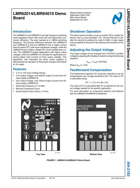
Top View<br />
30171502<br />
National Semiconductor<br />
<strong>Application</strong> <strong>Note</strong> <strong>2183</strong><br />
Marc Davis-Marsh<br />
September 22, 2011<br />
Shutdown Operation<br />
The demo board includes a pull-up resistor R3 to enable the<br />
device once V IN has exceeded 1.5V. Use the EN post to disable<br />
the device by pulling this node to GND. A logic signal<br />
may be applied to the post to test startup and shutdown of the<br />
device.<br />
Adjusting the Output Voltage<br />
The output voltage can be changed from 12V/24V to another<br />
voltage by adjusting the feedback resistors using the following<br />
equation:<br />
Where V FB is 1.23V.<br />
FIGURE 1. <strong>LMR62014</strong>/<strong>LMR64010</strong> <strong>Demo</strong> <strong>Board</strong><br />
V OUT = V FB (1+(R1/R2))<br />
Feedforward Compensation<br />
The feedforward capacitor CF should be selected to set the<br />
compensation zero at approximately 8 kHz. The value of CF<br />
is calculated using:<br />
CF = 1 / (2 x π x 8k x R1)<br />
The value of CF is calculated after R1 is selected for the output<br />
voltage needed for the specific application.<br />
For more information on component selection and features<br />
see the <strong>LMR62014</strong>/<strong>LMR64010</strong> datasheet.<br />
Bottom View<br />
© 2011 National Semiconductor Corporation 301715 www.national.com<br />
30171503<br />
<strong>LMR62014</strong>/<strong>LMR64010</strong> <strong>Demo</strong> <strong>Board</strong> AN-<strong>2183</strong>
AN-<strong>2183</strong><br />
30171501<br />
FIGURE 2. <strong>LMR62014</strong> <strong>Demo</strong> <strong>Board</strong> Schematic<br />
Bill of Materials (BOM) <strong>LMR62014</strong><br />
ID Part Number Type Size Parameters Qty Vendor<br />
U1 <strong>LMR62014</strong>XMF-ADJ Boost Regulator SOT-23 1 NSC<br />
L1 NR6045T100M Inductor SMD 10uH, 2.5A, 0.061<br />
ohm,<br />
D1 CRS08 Diode S-Flat Schottky, 30V,<br />
1.5A<br />
C1 GRM21BR71C225KA12L Capacitor 0805 Ceramic, 2.2uF,<br />
16V, X7R<br />
C2 GRM32ER71H475KA88L Capacitor 1210 Ceramic, 4.7uF,<br />
50V, X7R<br />
CF C0603C221J5GACTU Capacitor 0603 Ceramic, 220pF,<br />
50V, C0G/NP0<br />
CHF GRM188R71H223KA01D Capacitor 0603 Ceramic,<br />
0.022uF, 50V,<br />
X7R<br />
1 Sumida<br />
1 Toshiba<br />
1 Murata<br />
1 Murata<br />
1 Kemet<br />
1 Murata<br />
R1 CRCW0603115KFKEA Resistor 0603 115 kΩ 1 Vishay<br />
R2 CRCW060313K3FKEA Resistor 0603 13.3 kΩ 1 Vishay<br />
R3 CRCW06031M00JNEA Resistor 0603 1.0 MegΩ 1 Vishay<br />
EN 5014 Test Point Loop Yellow 1 Keystone<br />
VIN 5010 Test Point Loop Red 1 Keystone<br />
VOUT 5013 Test Point Loop Orange 1 Keystone<br />
GND 5011 Test Point Loop Black 2 Keystone<br />
www.national.com 2
AN-<strong>2183</strong><br />
30171501<br />
FIGURE 3. <strong>LMR64010</strong> <strong>Demo</strong> <strong>Board</strong> Schematic<br />
Bill of Materials (BOM) <strong>LMR64010</strong><br />
ID Part Number Type Size Parameters Qty Vendor<br />
U1 <strong>LMR64010</strong>XMF-ADJ Boost Regulator SOT-23 1 NSC<br />
L1 NR6045T100M Inductor SMD 10uH, 2.5A, 0.061<br />
ohm,<br />
D1 CRS04 Diode S-Flat Schottky, 40V,<br />
1.0A<br />
C1 GRM21BR71C225KA12L Capacitor 0805 Ceramic, 2.2uF,<br />
16V, X7R<br />
C2 GRM32ER71H475KA88L Capacitor 1210 Ceramic, 4.7uF,<br />
50V, X7R<br />
CF C0603C121J5GACTU Capacitor 0603 Ceramic, 120pF,<br />
50V, C0G/NP0<br />
CHF GRM188R71H223KA01D Capacitor 0603 Ceramic,<br />
0.022uF, 50V,<br />
X7R<br />
1 Sumida<br />
1 Toshiba<br />
1 Murata<br />
1 Murata<br />
1 Kemet<br />
1 Murata<br />
R1 CRCW0603243KFKEA Resistor 0603 243 kΩ 1 Vishay<br />
R2 CRCW060313K3FKEA Resistor 0603 13.3 kΩ 1 Vishay<br />
R3 CRCW06031M00JNEA Resistor 0603 1.0 MegΩ 1 Vishay<br />
EN 5014 Test Point Loop Yellow 1 Keystone<br />
VIN 5010 Test Point Loop Red 1 Keystone<br />
VOUT 5013 Test Point Loop Orange 1 Keystone<br />
GND 5011 Test Point Loop Black 2 Keystone<br />
3 www.national.com
AN-<strong>2183</strong><br />
Test Setup<br />
Step <strong>Demo</strong>nstration <strong>Board</strong> Quick Setup Procedures <strong>LMR62014</strong> <strong>Note</strong>s<br />
1 Connect a power supply to VIN terminals<br />
2 Connect a load to VOUT terminals<br />
3 EN terminal should be left floating for normal operation. Short this to ground<br />
to shutdown the part<br />
4 Set VIN = 5V, with 0A load applied, check VOUT with a voltmeter Nominal 11.9V<br />
5 Apply a 450mA load and check VOUT Nominal 11.9V<br />
Step <strong>Demo</strong>nstration <strong>Board</strong> Quick Setup Procedures <strong>LMR64010</strong> <strong>Note</strong>s<br />
1 Connect a power supply to VIN terminals<br />
2 Connect a load to VOUT terminals<br />
3 EN terminal should be left floating for normal operation. Short this to ground<br />
to shutdown the part<br />
4 Set VIN = 5V, with 0A load applied, check VOUT with a voltmeter Nominal 23.7V<br />
5 Apply a 125mA load and check VOUT Nominal 23.5V<br />
Efficiency Measurements<br />
Edge Connector Schematic<br />
Voltage Ripple Measurements<br />
30171505<br />
30171507<br />
30171506<br />
www.national.com 4
Typical Performance Characteristics<br />
Efficiency vs. Load Current <strong>LMR62014</strong>, VOUT = 12V<br />
95<br />
90<br />
EFFICIENCY (%)<br />
85<br />
80<br />
75<br />
70<br />
65<br />
VIN =5.0V<br />
60<br />
0.0 0.1 0.2 0.3 0.4 0.5<br />
LOAD CURRENT (A)<br />
30171508<br />
Efficiency vs. Load Current <strong>LMR64010</strong>, VOUT = 24V<br />
95<br />
90<br />
Efficiency vs. Load Current <strong>LMR62014</strong>, VOUT = 12V<br />
85<br />
80<br />
75<br />
EFFICIENCY (%)<br />
70<br />
65<br />
60<br />
55<br />
50<br />
45<br />
VIN =3.3V<br />
40<br />
0.00 0.05 0.10<br />
LOAD CURRENT (A)<br />
30171517<br />
Efficiency vs. Load Current <strong>LMR64010</strong>, VOUT = 24V<br />
95<br />
90<br />
AN-<strong>2183</strong><br />
EFFICIENCY (%)<br />
85<br />
80<br />
75<br />
70<br />
EFFICIENCY (%)<br />
85<br />
80<br />
75<br />
70<br />
65<br />
65<br />
60<br />
VIN =12.0V<br />
60<br />
VIN = 5.0V<br />
0.00 0.05 0.10 0.15 0.20 0.25 0.30 0.35<br />
LOAD CURRENT (A)<br />
0.000 0.025 0.050 0.075 0.100 0.125<br />
LOAD CURRENT (A)<br />
30171509<br />
30171518<br />
Load Transient Waveforms <strong>LMR62014</strong><br />
IOUT = 33 to 330mA<br />
Load Transient Waveforms <strong>LMR64010</strong><br />
IOUT = 13 to 125mA<br />
30171510<br />
30171511<br />
5 www.national.com
AN-<strong>2183</strong><br />
Switching Node and Output Voltage Waveforms<br />
<strong>LMR62014</strong><br />
Switching Node and Output Voltage Waveforms<br />
<strong>LMR64010</strong><br />
Startup Waveform<br />
30171512<br />
30171513<br />
30171514<br />
www.national.com 6
Layout<br />
AN-<strong>2183</strong><br />
Top Layer<br />
30171515<br />
Top Overlay<br />
30171519<br />
7 www.national.com
AN-<strong>2183</strong><br />
Bottom Layer<br />
30171516<br />
Bottom Overlay<br />
30171520<br />
www.national.com 8
9 www.national.com<br />
AN-<strong>2183</strong>
AN-<strong>2183</strong> <strong>LMR62014</strong>/<strong>LMR64010</strong> <strong>Demo</strong> <strong>Board</strong><br />
<strong>Note</strong>s<br />
For more National Semiconductor product information and proven design tools, visit the following Web sites at:<br />
www.national.com<br />
Products<br />
Design Support<br />
Amplifiers www.national.com/amplifiers WEBENCH® Tools www.national.com/webench<br />
Audio www.national.com/audio App <strong>Note</strong>s www.national.com/appnotes<br />
Clock and Timing www.national.com/timing Reference Designs www.national.com/refdesigns<br />
Data Converters www.national.com/adc Samples www.national.com/samples<br />
Interface www.national.com/interface Eval <strong>Board</strong>s www.national.com/evalboards<br />
LVDS www.national.com/lvds Packaging www.national.com/packaging<br />
Power Management www.national.com/power Green Compliance www.national.com/quality/green<br />
Switching Regulators www.national.com/switchers Distributors www.national.com/contacts<br />
LDOs www.national.com/ldo Quality and Reliability www.national.com/quality<br />
LED Lighting www.national.com/led Feedback/Support www.national.com/feedback<br />
Voltage References www.national.com/vref Design Made Easy www.national.com/easy<br />
PowerWise® Solutions www.national.com/powerwise <strong>Application</strong>s & Markets www.national.com/solutions<br />
Serial Digital Interface (SDI) www.national.com/sdi Mil/Aero www.national.com/milaero<br />
Temperature Sensors www.national.com/tempsensors SolarMagic www.national.com/solarmagic<br />
PLL/VCO www.national.com/wireless PowerWise® Design<br />
University<br />
www.national.com/training<br />
THE CONTENTS OF THIS DOCUMENT ARE PROVIDED IN CONNECTION WITH NATIONAL SEMICONDUCTOR CORPORATION<br />
(“NATIONAL”) PRODUCTS. NATIONAL MAKES NO REPRESENTATIONS OR WARRANTIES WITH RESPECT TO THE ACCURACY<br />
OR COMPLETENESS OF THE CONTENTS OF THIS PUBLICATION AND RESERVES THE RIGHT TO MAKE CHANGES TO<br />
SPECIFICATIONS AND PRODUCT DESCRIPTIONS AT ANY TIME WITHOUT NOTICE. NO LICENSE, WHETHER EXPRESS,<br />
IMPLIED, ARISING BY ESTOPPEL OR OTHERWISE, TO ANY INTELLECTUAL PROPERTY RIGHTS IS GRANTED BY THIS<br />
DOCUMENT.<br />
TESTING AND OTHER QUALITY CONTROLS ARE USED TO THE EXTENT NATIONAL DEEMS NECESSARY TO SUPPORT<br />
NATIONAL’S PRODUCT WARRANTY. EXCEPT WHERE MANDATED BY GOVERNMENT REQUIREMENTS, TESTING OF ALL<br />
PARAMETERS OF EACH PRODUCT IS NOT NECESSARILY PERFORMED. NATIONAL ASSUMES NO LIABILITY FOR<br />
APPLICATIONS ASSISTANCE OR BUYER PRODUCT DESIGN. BUYERS ARE RESPONSIBLE FOR THEIR PRODUCTS AND<br />
APPLICATIONS USING NATIONAL COMPONENTS. PRIOR TO USING OR DISTRIBUTING ANY PRODUCTS THAT INCLUDE<br />
NATIONAL COMPONENTS, BUYERS SHOULD PROVIDE ADEQUATE DESIGN, TESTING AND OPERATING SAFEGUARDS.<br />
EXCEPT AS PROVIDED IN NATIONAL’S TERMS AND CONDITIONS OF SALE FOR SUCH PRODUCTS, NATIONAL ASSUMES NO<br />
LIABILITY WHATSOEVER, AND NATIONAL DISCLAIMS ANY EXPRESS OR IMPLIED WARRANTY RELATING TO THE SALE<br />
AND/OR USE OF NATIONAL PRODUCTS INCLUDING LIABILITY OR WARRANTIES RELATING TO FITNESS FOR A PARTICULAR<br />
PURPOSE, MERCHANTABILITY, OR INFRINGEMENT OF ANY PATENT, COPYRIGHT OR OTHER INTELLECTUAL PROPERTY<br />
RIGHT.<br />
LIFE SUPPORT POLICY<br />
NATIONAL’S PRODUCTS ARE NOT AUTHORIZED FOR USE AS CRITICAL COMPONENTS IN LIFE SUPPORT DEVICES OR<br />
SYSTEMS WITHOUT THE EXPRESS PRIOR WRITTEN APPROVAL OF THE CHIEF EXECUTIVE OFFICER AND GENERAL<br />
COUNSEL OF NATIONAL SEMICONDUCTOR CORPORATION. As used herein:<br />
Life support devices or systems are devices which (a) are intended for surgical implant into the body, or (b) support or sustain life and<br />
whose failure to perform when properly used in accordance with instructions for use provided in the labeling can be reasonably expected<br />
to result in a significant injury to the user. A critical component is any component in a life support device or system whose failure to perform<br />
can be reasonably expected to cause the failure of the life support device or system or to affect its safety or effectiveness.<br />
National Semiconductor and the National Semiconductor logo are registered trademarks of National Semiconductor Corporation. All other<br />
brand or product names may be trademarks or registered trademarks of their respective holders.<br />
Copyright© 2011 National Semiconductor Corporation<br />
For the most current product information visit us at www.national.com<br />
www.national.com<br />
National Semiconductor<br />
Americas Technical<br />
Support Center<br />
Email: support@nsc.com<br />
Tel: 1-800-272-9959<br />
National Semiconductor Europe<br />
Technical Support Center<br />
Email: europe.support@nsc.com<br />
National Semiconductor Asia<br />
Pacific Technical Support Center<br />
Email: ap.support@nsc.com<br />
National Semiconductor Japan<br />
Technical Support Center<br />
Email: jpn.feedback@nsc.com


