

LM21215A-1 15A High Efficiency Synchronous Buck Regulator with ...
LM21215A-1 15A High Efficiency Synchronous Buck Regulator with ...
LM21215A-1 15A High Efficiency Synchronous Buck Regulator with ...

You also want an ePaper? Increase the reach of your titles
YUMPU automatically turns print PDFs into web optimized ePapers that Google loves.
<strong>LM212<strong>15A</strong></strong>-1<br />
March 27, 2011<br />
<strong>15A</strong> <strong>High</strong> <strong>Efficiency</strong> <strong>Synchronous</strong> <strong>Buck</strong> <strong>Regulator</strong> <strong>with</strong><br />
Frequency Synchronization<br />
General Description<br />
The <strong>LM212<strong>15A</strong></strong>-1 is a monolithic synchronous buck regulator<br />
that is capable of delivering up to <strong>15A</strong> of continuous output<br />
current while producing an output voltage down to 0.6V <strong>with</strong><br />
outstanding efficiency. The device is optimized to work over<br />
an input voltage range of 2.95V to 5.5V, making it suited for<br />
a wide variety of low voltage systems. The voltage mode control<br />
loop provides high noise immunity, narrow duty cycle<br />
capability and can be compensated to be stable <strong>with</strong> any type<br />
of output capacitance, providing maximum flexibility and ease<br />
of use.<br />
The <strong>LM212<strong>15A</strong></strong>-1 features internal over voltage protection<br />
(OVP) and over-current protection (OCP) for increased system<br />
reliability. A precision enable pin and integrated UVLO<br />
allow turn-on of the device to be tightly controlled and sequenced.<br />
Startup inrush currents are limited by both an internally<br />
fixed and externally adjustable soft-start circuit. Fault<br />
detection and supply sequencing are possible <strong>with</strong> the integrated<br />
power good circuit.<br />
The <strong>LM212<strong>15A</strong></strong>-1 is designed to work well in multi-rail power<br />
supply architectures. The output voltage of the device can be<br />
configured to track an external voltage rail using the SS/TRK<br />
pin. The switching frequency can be synchronized to the<br />
falling edge of a clock between frequencies of 300kHz to<br />
1.5MHz.<br />
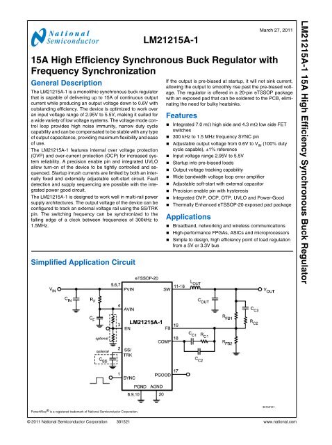
Simplified Application Circuit<br />
If the output is pre-biased at startup, it will not sink current,<br />
allowing the output to smoothly rise past the pre-biased voltage.<br />
The regulator is offered in a 20-pin eTSSOP package<br />
<strong>with</strong> an exposed pad that can be soldered to the PCB, eliminating<br />
the need for bulky heatsinks.<br />
Features<br />
■ Integrated 7.0 mΩ high side and 4.3 mΩ low side FET<br />
switches<br />
■ 300 kHz to 1.5 MHz frequency SYNC pin<br />
■ Adjustable output voltage from 0.6V to V IN (100% duty<br />
cycle capable), ±1% reference<br />
■ Input voltage range 2.95V to 5.5V<br />
■ Startup into pre-biased loads<br />
■ Output voltage tracking capability<br />
■ Wide bandwidth voltage loop error amplifier<br />
■ Adjustable soft-start <strong>with</strong> external capacitor<br />
■ Precision enable pin <strong>with</strong> hysteresis<br />
■ Integrated OVP, OCP, OTP, UVLO and Power-Good<br />
■ Thermally Enhanced eTSSOP-20 exposed pad package<br />
Applications<br />
■ Broadband, networking and wireless communications<br />
■ <strong>High</strong>-performance FPGAs, ASICs and microprocessors<br />
■ Simple to design, high efficiency point of load regulation<br />
from a 5V or 3.3V bus<br />
<strong>LM212<strong>15A</strong></strong>-1 <strong>15A</strong> <strong>High</strong> <strong>Efficiency</strong> <strong>Synchronous</strong> <strong>Buck</strong> <strong>Regulator</strong><br />
PowerWise ® is a registered trademark of National Semiconductor Corporation.<br />
30152101<br />
© 2011 National Semiconductor Corporation 301521 www.national.com
<strong>LM212<strong>15A</strong></strong>-1<br />
Connection Diagram<br />
Top View<br />
eTSSOP-20 Package<br />
30152102<br />
Ordering Information<br />
Order Number Package Type NSC Package Drawing Package Marking Supplied As<br />
<strong>LM212<strong>15A</strong></strong>MH-1 eTSSOP-20 MYB20A <strong>LM212<strong>15A</strong></strong>MH-1 73 Units per Rail<br />
<strong>LM212<strong>15A</strong></strong>MHX-1 eTSSOP-20 MYB20A <strong>LM212<strong>15A</strong></strong>MH-1 2500 Units Per Reel<br />
<strong>LM212<strong>15A</strong></strong>MHE-1 eTSSOP-20 MYB20A <strong>LM212<strong>15A</strong></strong>MH-1 250 Units Per Reel<br />
Pin Descriptions<br />
Pins Name Description<br />
1 SYNC Frequency Synchronization input pin. Applying a clock signal to this pin will force<br />
the device to switch at the clock frequency. If left unconnected, the frequency will<br />
default to 500 kHz.<br />
2 SS/TRK Soft-start control pin. An internal 2 µA current source charges an external capacitor<br />
connected between this pin and AGND to set the output voltage ramp rate during<br />
startup. This pin can also be used to configure the tracking feature.<br />
3 EN Active high enable input for the device. If not used, the EN pin can be left open,<br />
which will go high due to an internal current source.<br />
4 AVIN Analog input voltage supply that generates the internal bias. It is recommended to<br />
connect PVIN to AVIN through a low pass RC filter to minimize the influence of<br />
input rail ripple and noise on the analog control circuitry.<br />
5,6,7 PVIN Input voltage to the power switches inside the device. These pins should be<br />
connected together at the device. A low ESR input capacitance should be located<br />
as close as possible to these pins.<br />
8,9,10 PGND Power ground pins for the internal power switches.<br />
11-16 SW Switch node pins. These pins should be tied together locally and connected to the<br />
filter inductor.<br />
17 PGOOD Open-drain power good indicator.<br />
18 COMP Compensation pin is connected to the output of the voltage loop error amplifier.<br />
19 FB Feedback pin is connected to the inverting input of the voltage loop error amplifier.<br />
20 AGND Quiet analog ground for the internal reference and bias circuitry.<br />
EP Exposed Pad Exposed metal pad on the underside of the package <strong>with</strong> an electrical and thermal<br />
connection to PGND. It is recommended to connect this pad to the PC board<br />
ground plane in order to improve thermal dissipation.<br />
www.national.com 2
Absolute Maximum Ratings (Note 1)<br />
If Military/Aerospace specified devices are required,<br />
please contact the National Semiconductor Sales Office/<br />
Distributors for availability and specifications.<br />
PVIN(Note 2), AVIN to GND −0.3V to +6V<br />
SW(Note 3), EN, FB, COMP, −0.3V to PVIN + 0.3V<br />
PGOOD, SS/TRK to GND<br />
ESD Rating<br />
Human Body Model (Note 4)<br />
Operating Ratings (Note 1)<br />
PVIN, AVIN to GND<br />
Junction Temperature<br />
θ JA (Note 5)<br />
2kV<br />
+2.95V to +5.5V<br />
−40°C to +125°C<br />
24°C/W<br />
<strong>LM212<strong>15A</strong></strong>-1<br />
Storage Temperature −65°C to 150°C<br />
Soldering Specification for<br />
TSSOP Pb-Free Infrared or<br />
Convection (30 sec)<br />
260°C<br />
Electrical Characteristics Unless otherwise stated, the following conditions apply: V PVIN, AVIN = 5V. Limits in<br />
standard type are for T J = 25°C only, limits in bold face type apply over the junction temperature (T J ) range of −40°C to +125°C.<br />
Minimum and maximum limits are guaranteed through test, design, or statistical correlation. Typical values represent the most<br />
likely parametric norm at T J = 25°C, and are provided for reference purposes only.<br />
Symbol Parameter Conditions Min Typ Max Units<br />
SYSTEM<br />
V FB Feedback pin voltage V IN = 2.95V to 5.5V -1% 0.6 1% V<br />
ΔV OUT /ΔI OUT<br />
Load Regulation 0.02 %V OUT /<br />
A<br />
ΔV OUT /ΔV IN<br />
Line Regulation 0.1 %V OUT /<br />
V<br />
R DSON HS <strong>High</strong> Side Switch On Resistance I SW = 12A 7.0 9.0 mΩ<br />
R DSON LS Low Side Switch On Resistance I SW = 12A 4.3 6.0 mΩ<br />
I CLR HS Rising Switch Current Limit 17.3 20 22.8 A<br />
I CLF LS Falling Switch Current Limit 14 A<br />
V ZX Zero Cross Voltage -8 3 12 mV<br />
I Q Operating Quiescent Current 1.5 3.0 mA<br />
I SD Shutdown Quiescent Current V EN = 0V 50 70 µA<br />
V UVLO AVIN Under Voltage Lockout AVIN Rising 2.45 2.70 2.95 V<br />
V UVLOHYS AVIN Under Voltage Lockout Hysteresis 140 200 280 mV<br />
V TRACKOS SS/TRACK PIN accuracy (V SS - V FB ) 0 < V TRACK < 0.55V -10 6 20 mV<br />
I SS Soft-Start Pin Source Current 1.3 1.9 2.5 µA<br />
t INTSS Internal Soft-Start Ramp to Vref C SS = 0 350 500 675 µs<br />
t RESETSS Device Reset to Soft-Start Ramp 50 110 200 µs<br />
OSCILLATOR<br />
f SYNCR SYNC Frequency Range 300 1500 kHz<br />
f DEFAULT Default (no SYNC signal) Frequency 475 500 525 kHz<br />
t SY_SW Time from SYNC falling to V SW Rising 200 ns<br />
t SY_MIN Minimum SYNC pin pulse width, high or low 100 ns<br />
t HSBLANK HS OCP Blanking Time Rising edge of SW to I CLR<br />
comparison<br />
t LSBLANK LS OCP Blanking Time Falling edge of SW to I CLF<br />
comparison<br />
t ZXBLANK Zero Cross Blanking Time Falling edge of SW to V ZX<br />
comparison<br />
55 ns<br />
400 ns<br />
120 ns<br />
t MINON Minimum HS on-time 140 ns<br />
ΔVramp PWM Ramp p-p Voltage 0.8 V<br />
ERROR AMPLIFIER<br />
V OL Error Amplifier Open Loop Voltage Gain ICOMP = -65µA to 1mA 95 dBV/V<br />
GBW Error Amplifier Gain-Bandwidth Product 11 MHz<br />
3 www.national.com
<strong>LM212<strong>15A</strong></strong>-1<br />
Symbol Parameter Conditions Min Typ Max Units<br />
SYSTEM<br />
I FB Feedback Pin Bias Current V FB = 0.6V 1 nA<br />
I COMPSRC COMP Output Source Current 1 mA<br />
I COMPSINK COMP Output Sink Current 65 µA<br />
POWERGOOD<br />
V OVP Over Voltage Protection Rising Threshold V FB Rising 105 112.5 120 %V FB<br />
V OVPHYS Over Voltage Protection Hysteresis V FB Falling 2 %V FB<br />
V UVP Under Voltage Protection Rising Threshold V FB Rising 82 90 97 %V FB<br />
V UVPHYS Under Voltage Protection Hysteresis V FB Falling 2.5 %V FB<br />
t PGDGL PGOOD Deglitch Low (OVP/UVP Condition<br />
Duration to PGOOD Falling)<br />
15 µs<br />
t PGDGH PGOOD Deglitch <strong>High</strong> (minimum low pulse) 12 µs<br />
R PGOOD PGOOD Pull-down Resistance 10 20 40 Ω<br />
I PGOODLEAK PGOOD Leakage Current V PGOOD = 5V 1 nA<br />
LOGIC<br />
V IHSYNC SYNC Pin Logic <strong>High</strong> 2.0 V<br />
V ILSYNC SYNC Pin Logic Low 0.8 V<br />
V IHENR EN Pin Rising Threshold V EN Rising 1.20 1.35 1.45 V<br />
V ENHYS EN Pin Hysteresis 50 110 180 mV<br />
I EN EN Pin Pullup Current V EN = 0V 2 µA<br />
THERMAL SHUTDOWN<br />
T THERMSD Thermal Shutdown 165 °C<br />
T THERMSDHYS Thermal Shutdown Hysteresis 10 °C<br />
Note 1: Absolute Maximum Ratings indicate limits beyond witch damage to the device may occur. Operating Ratings indicate conditions for which the device is<br />
intended to be functional, but do not guarantee specific performance limits. For guaranteed specifications and test conditions, see the Electrical Characteristics.<br />
Note 2: The PVIN pin can tolerate transient voltages up to 6.5 V for a period of up to 6ns. These transients can occur during the normal operation of the device.<br />
Note 3: The SW pin can tolerate transient voltages up to 9.0 V for a period of up to 6ns, and -1.0V for a duration of 4ns. These transients can occur during the<br />
normal operation of the device.<br />
Note 4: The human body model is a 100 pF capacitor discharged through a 1.5 kΩ resistor to each pin.<br />
Note 5: Thermal measurements were performed on a 2x2 inch, 4 layer, 2 oz. copper outer layer, 1 oz.copper inner layer board <strong>with</strong> twelve 8 mil. vias underneath<br />
the EP of the device and an additional sixteen 8 mil. vias under the unexposed package.<br />
www.national.com 4
Typical Performance Characteristics Unless otherwise specified: V VIN = 5V, V OUT = 1.2V, L= 0.56µH<br />
(1.8mΩ R DCR ), C SS = 33nF, f SW = 500 kHz, T A = 25°C for efficiency curves, loop gain plots and waveforms, and T J = 25°C for all<br />
others.<br />
EFFICIENCY (%)<br />
100<br />
98<br />
96<br />
94<br />
92<br />
90<br />
88<br />
86<br />
84<br />
82<br />
80<br />
<strong>Efficiency</strong><br />
FSW = 500 kHz<br />
FSW = 750 kHz<br />
FSW = 1 MHz<br />
0 3 6 9 12 15<br />
OUTPUT CURRENT (A)<br />
EFFICIENCY (%)<br />
100<br />
98<br />
96<br />
94<br />
92<br />
90<br />
88<br />
86<br />
84<br />
82<br />
80<br />
<strong>Efficiency</strong><br />
VOUT = 1.2V<br />
VOUT = 3.3V<br />
0 3 6 9 12 15<br />
OUTPUT CURRENT (A)<br />
<strong>LM212<strong>15A</strong></strong>-1<br />
30152153<br />
30152156<br />
<strong>Efficiency</strong><br />
(VOUT = 2.5 V, f SW = 500 kHz , Inductor P/N SER2010-601MLD)<br />
100<br />
0.04<br />
0.03<br />
Load Regulation<br />
EFFICIENCY (%)<br />
98<br />
96<br />
94<br />
92<br />
90<br />
VIN = 3.3V<br />
VIN = 4.0V<br />
VIN = 5.0V<br />
VIN = 5.5V<br />
0 3 6 9 12 15<br />
OUTPUT CURRENT (A)<br />
Δ OUTPUT VOLTAGE (%)<br />
0.02<br />
0.01<br />
0.00<br />
-0.01<br />
-0.02<br />
-0.03 VIN = 3.3V<br />
VIN = 5.0V<br />
-0.04<br />
0 3 6 9 12 15<br />
OUTPUT CURRENT (A)<br />
30152154<br />
30152177<br />
Δ OUTPUT VOLTAGE (%)<br />
0.10<br />
0.08<br />
0.06<br />
0.04<br />
0.02<br />
0.00<br />
-0.02<br />
-0.04<br />
Line Regulation<br />
-0.06<br />
-0.08<br />
IOUT = 0A<br />
IOUT = 12A<br />
-0.10<br />
3.0 3.5 4.0 4.5 5.0 5.5<br />
INPUT VOLTAGE (V)<br />
30152155<br />
IPVIN + IAVIN (mA)<br />
1.5<br />
1.4<br />
1.3<br />
1.2<br />
1.1<br />
Non-Switching I QTOTAL vs. V IN<br />
1.0<br />
3.0 3.5 4.0 4.5 5.0 5.5<br />
INPUT VOLTAGE (V)<br />
30152157<br />
5 www.national.com
<strong>LM212<strong>15A</strong></strong>-1<br />
Non-Switching I AVIN and I PVIN vs. Temperature<br />
IAVIN (mA)<br />
1.20<br />
1.17<br />
1.14<br />
1.11<br />
1.08<br />
1.05<br />
1.02<br />
0.99<br />
0.96<br />
0.93<br />
IAVIN<br />
IPVIN<br />
0.180<br />
0.172<br />
0.164<br />
0.156<br />
0.148<br />
0.140<br />
0.132<br />
0.124<br />
0.116<br />
0.108<br />
0.90<br />
0.100<br />
-40 -20 0 20 40 60 80 100 120<br />
JUNCTION TEMPERATURE (°C)<br />
IPVIN (mA)<br />
Enable Threshold and Hysteresis vs. Temperature<br />
VIHENR (V)<br />
SHUTDOWN CURRENT ISD (μA)<br />
1.37<br />
1.36<br />
1.35<br />
1.34<br />
1.33<br />
1.32<br />
1.31<br />
1.30<br />
1.29<br />
1.28<br />
V IHENR<br />
V ENHYS<br />
-40 -20 0 20 40 60 80 100 120<br />
JUNCTION TEMPERATURE (°C)<br />
Enable Low Current vs. Temperature<br />
60<br />
58<br />
56<br />
54<br />
52<br />
50<br />
48<br />
46<br />
44<br />
42<br />
40<br />
160<br />
152<br />
144<br />
136<br />
128<br />
120<br />
112<br />
104<br />
96<br />
88<br />
80<br />
30152175<br />
VENHYS (V)<br />
-40 -20 0 20 40 60 80 100 120<br />
JUNCTION TEMPERATURE (°C)<br />
30152171<br />
30152173<br />
VFB (V)<br />
0.602<br />
0.601<br />
0.600<br />
0.599<br />
0.598<br />
V FB vs. Temperature<br />
-40 -20 0 20 40 60 80 100 120<br />
JUNCTION TEMPERATURE (°C)<br />
30152176<br />
UVLO Threshold and Hysteresis vs. Temperature<br />
VUVLO (V)<br />
VOVP ,VUVP (V)<br />
2.80<br />
2.78<br />
2.76<br />
2.74<br />
2.72<br />
2.70<br />
2.68<br />
2.66<br />
2.64<br />
2.62<br />
2.60<br />
V UVLO<br />
V UVLOHYS<br />
-40 -20 0 20 40 60 80 100 120<br />
JUNCTION TEMPERATURE (°C)<br />
OVP/UVP Threshold vs. Temperature<br />
0.68<br />
0.66<br />
0.64<br />
0.62<br />
0.60<br />
0.58<br />
0.57<br />
0.54<br />
0.52<br />
VUVP<br />
VOVP<br />
300<br />
285<br />
270<br />
255<br />
240<br />
225<br />
210<br />
195<br />
180<br />
165<br />
150<br />
0.50<br />
-40 -20 0 20 40 60 80 100 120<br />
JUNCTION TEMPERATURE (°C)<br />
VUVLOHYS (mV)<br />
30152170<br />
30152174<br />
www.national.com 6
MINIMUM ON-TIME (nS)<br />
Minimum On-Time vs. Temperature<br />
160<br />
156<br />
152<br />
148<br />
144<br />
140<br />
136<br />
132<br />
128<br />
124<br />
RDSON (mΩ)<br />
FET Resistance vs. Temperature<br />
10<br />
9<br />
8<br />
7<br />
6<br />
5<br />
4<br />
3<br />
LOW SIDE<br />
HIGH SIDE<br />
<strong>LM212<strong>15A</strong></strong>-1<br />
120<br />
2<br />
-40 -20 0 20 40 60 80 100 120<br />
JUNCTION TEMPERATURE (°C)<br />
-40 -20 0 20 40 60 80 100 120<br />
JUNCTION TEMPERATURE (°C)<br />
30152172<br />
30152168<br />
Peak Current Limit vs. Temperature<br />
SYNC Signal Lost<br />
CURRENT LIMIT ICLR (A)<br />
19.6<br />
19.5<br />
19.4<br />
19.3<br />
19.2<br />
19.1<br />
19.0<br />
18.9<br />
18.8<br />
18.7<br />
-40 -20 0 20 40 60 80 100 120<br />
AMBIENT TEMPERATURE (°C)<br />
SYNC Signal Acquired<br />
30152158<br />
4 µs/DIV<br />
Load Transient Response<br />
30152165<br />
10 µs/DIV<br />
30152160<br />
100 µs/DIV<br />
30152161<br />
7 www.national.com
<strong>LM212<strong>15A</strong></strong>-1<br />
Output Voltage Ripple<br />
Startup <strong>with</strong> Prebiased Output<br />
2 µs/DIV<br />
30152164<br />
2 ms/DIV<br />
30152163<br />
Startup <strong>with</strong> SS/TRK Open Circuit<br />
Startup <strong>with</strong> applied Track Signal<br />
200 µs/DIV<br />
30152166<br />
200 ms/DIV<br />
30152167<br />
Output Over-Current Condition<br />
10 µs/DIV<br />
30152180<br />
www.national.com 8
Block Diagram<br />
<strong>LM212<strong>15A</strong></strong>-1<br />
30152103<br />
9 www.national.com
<strong>LM212<strong>15A</strong></strong>-1<br />
Operation Description<br />
GENERAL<br />
The <strong>LM212<strong>15A</strong></strong>-1 switching regulator features all of the functions<br />
necessary to implement an efficient low voltage buck<br />
regulator using a minimum number of external components.<br />
This easy to use regulator features two integrated switches<br />
and is capable of supplying up to <strong>15A</strong> of continuous output<br />
current. The regulator utilizes voltage mode control <strong>with</strong> trailing<br />
edge modulation to optimize stability and transient response<br />
over the entire output voltage range. The device can<br />
operate at high switching frequency allowing use of a small<br />
inductor while still achieving high efficiency. The precision internal<br />
voltage reference allows the output to be set as low as<br />
0.6V. Fault protection features include: current limiting, thermal<br />
shutdown, over voltage protection, and shutdown capability.<br />
The device is available in the eTSSOP-20 package<br />
featuring an exposed pad to aid thermal dissipation. The<br />
<strong>LM212<strong>15A</strong></strong>-1 can be used in numerous applications to efficiently<br />
step-down from a 5V or 3.3V bus.<br />
FREQUENCY SYNCHRONIZATION<br />
The sync (SYNC) pin allows the <strong>LM212<strong>15A</strong></strong>-1 to be switched<br />
at an external clock frequency. When a clock signal is present<br />
on the SYNC pin <strong>with</strong>in the allowable frequency range, 300<br />
kHz to 1.5 MHz, the device will synchronize the turn-on of the<br />
high side FET (switch rising) to the negative edge of the clock<br />
signal, as seen in Figure 1 . If no clock signal is present, the<br />
<strong>LM212<strong>15A</strong></strong>-1 will default to a switching frequency of 500 kHz.<br />
The clock signal can be present on the SYNC pin before the<br />
device is powered on <strong>with</strong> no loading on the clock signal. Alternatively,<br />
if no clock is present while the device is powered<br />
up, it will begin switching at the default frequency of 500 kHz.<br />
Once the clock signal is present, the device will begin synchronizing<br />
to the clock frequency. The length of time necessary<br />
for the synchronization depends on the clock frequency.<br />
PRECISION ENABLE<br />
The enable (EN) pin allows the output of the device to be enabled<br />
or disabled <strong>with</strong> an external control signal. This pin is a<br />
precision analog input that enables the device when the voltage<br />
exceeds 1.35V (typical). The EN pin has 110 mV of<br />
hysteresis and will disable the output when the enable voltage<br />
falls below 1.24V (typical). If the EN pin is not used, it can be<br />
left open, and will be pulled high by an internal 2 µA current<br />
source. Since the enable pin has a precise turn-on threshold<br />
it can be used along <strong>with</strong> an external resistor divider network<br />
from VIN to configure the device to turn-on at a precise input<br />
voltage.<br />
UVLO<br />
The <strong>LM212<strong>15A</strong></strong>-1 has a built-in under-voltage lockout protection<br />
circuit that keeps the device from switching until the input<br />
voltage reaches 2.7V (typical). The UVLO threshold has 200<br />
mV of hysteresis that keeps the device from responding to<br />
power-on glitches during start up. If desired the turn-on point<br />
of the supply can be changed by using the precision enable<br />
pin and a resistor divider network connected to VIN as shown<br />
in Figure 6 in the design guide.<br />
CURRENT LIMIT<br />
The <strong>LM212<strong>15A</strong></strong>-1 has current limit protection to avoid dangerous<br />
current levels on the power FETs and inductor. A<br />
current limit condition is met when the current through the high<br />
side FET exceeds the rising current limit level (I CLR ). The control<br />
circuitry will respond to this event by turning off the high<br />
side FET and turning on the low side FET. This forces a negative<br />
voltage on the inductor, thereby causing the inductor<br />
current to decrease. The high side FET will not conduct again<br />
until the lower current limit level (I CLF ) is sensed on the low<br />
side FET. At this point, the device will resume normal switching.<br />
A current limit condition will cause the internal soft-start voltage<br />
to ramp downward. After the internal soft-start ramps<br />
below the Feedback (FB) pin voltage, (nominally 0.6 V), FB<br />
will begin to ramp downward, as well. This voltage foldback<br />
will limit the power consumption in the device, thereby protecting<br />
the device from continuously supplying power to the<br />
load under a condition that does not fall <strong>with</strong>in the device<br />
SOA. After the current limit condition is cleared, the internal<br />
soft-start voltage will ramp up again. Figure 2 shows current<br />
limit behavior <strong>with</strong> V SS , V FB , V OUT and V SW .<br />
30152133<br />
FIGURE 1. Frequency synchronization<br />
www.national.com 10
SHORT-CIRCUIT PROTECTION<br />
In the unfortunate event that the output is shorted <strong>with</strong> a low<br />
impedance to ground, the <strong>LM212<strong>15A</strong></strong>-1 will limit the current<br />
into the short by resetting the device. A short-circuit condition<br />
is sensed by a current-limit condition coinciding <strong>with</strong> a voltage<br />
on the FB pin that is lower than 100 mV. When this condition<br />
occurs, the device will begin its reset sequence, turning off<br />
both power FETs and discharging the soft-start capacitor after<br />
t RESETSS (nominally 110 µs). The device will then attempt to<br />
restart. If the short-circuit condition still exists, it will reset<br />
again, and repeat until the short-circuit is cleared. The reset<br />
prevents excess current flowing through the FETs in a highly<br />
inefficient manner, potentially causing thermal damage to the<br />
device or the bus supply.<br />
<strong>LM212<strong>15A</strong></strong>-1<br />
30152119<br />
FIGURE 2. Current Limit Conditions<br />
THERMAL PROTECTION<br />
Internal thermal shutdown circuitry is provided to protect the<br />
integrated circuit in the event that the maximum junction temperature<br />
is exceeded. When activated, typically at 165°C, the<br />
<strong>LM212<strong>15A</strong></strong>-1 tri-states the power FETs and resets soft start.<br />
After the junction cools to approximately 155°C, the device<br />
starts up using the normal start up routine. This feature is<br />
provided to prevent catastrophic failures from accidental device<br />
overheating. Note that thermal limit will not stop the die<br />
from operating above the specified operating maximum temperature,125°C.<br />
The die should be kept under 125°C to guarantee<br />
correct operation.<br />
POWERGOOD FLAG<br />
The PGOOD pin provides the user <strong>with</strong> a way to monitor the<br />
status of the <strong>LM212<strong>15A</strong></strong>-1. In order to use the PGOOD pin,<br />
the application must provide a pull-up resistor to a desired DC<br />
voltage (i.e. Vin). PGOOD will respond to a fault condition by<br />
pulling the PGOOD pin low <strong>with</strong> the open-drain output.<br />
PGOOD will pull low on the following conditions – 1) V FB<br />
moves above or below the V OVP or V UVP , respectively 2) The<br />
enable pin is brought below the enable threshold 3) The device<br />
enters a pre-biased output condition (V FB >V SS ).<br />
Figure 3 shows the conditions that will cause PGOOD to fall.<br />
11 www.national.com
<strong>LM212<strong>15A</strong></strong>-1<br />
30152118<br />
FIGURE 3. PGOOD Conditions<br />
LIGHT LOAD OPERATION<br />
The <strong>LM212<strong>15A</strong></strong>-1 offers increased efficiency when operating<br />
at light loads. Whenever the load current is reduced to a point<br />
where the peak to peak inductor ripple current is greater than<br />
two times the load current, the device will enter the diode emulation<br />
mode preventing significant negative inductor current.<br />
The output current at which this occurs is the critical conduction<br />
boundary and can be calculated by the following equation:<br />
It can be seen that in diode emulation mode, whenever the<br />
inductor current reaches zero the SW node will become high<br />
impedance. Ringing will occur on this pin as a result of the LC<br />
tank circuit formed by the inductor and the parasitic capacitance<br />
at the node. If this ringing is of concern an additional<br />
RC snubber circuit can be added from the switch node to<br />
ground.<br />
At very light loads, usually below 500mA, several pulses may<br />
be skipped in between switching cycles, effectively reducing<br />
the switching frequency and further improving light-load efficiency.<br />
Several diagrams are shown in Figure 4 illustrating continuous<br />
conduction mode (CCM), discontinuous conduction<br />
mode (DCM), and the boundary condition.<br />
www.national.com 12
<strong>LM212<strong>15A</strong></strong>-1<br />
30152179<br />
FIGURE 4. Modes of Operation for <strong>LM212<strong>15A</strong></strong>-1<br />
13 www.national.com
<strong>LM212<strong>15A</strong></strong>-1<br />
Design Guide<br />
OUTPUT VOLTAGE<br />
The first step in designing the <strong>LM212<strong>15A</strong></strong>-1 application is setting<br />
the output voltage. This is done by using a voltage divider<br />
between V OUT and AGND, <strong>with</strong> the middle node connected to<br />
V FB . When operating under steady-state conditions, the<br />
<strong>LM212<strong>15A</strong></strong>-1 will force V OUT such that V FB is driven to 0.6 V.<br />
30152104<br />
FIGURE 5. Setting V OUT<br />
A good starting point for the lower feedback resistor, R FB2 , is<br />
10kΩ. R FB1 can then be calculated the following equation:<br />
In the above equation, R A is the resistor from V IN to enable,<br />
R B is the resistor from enable to ground, I EN is the internal<br />
enable pull-up current (2µA) and 1.35V is the fixed precision<br />
enable threshold voltage. Typical values for R B range from<br />
10kΩ to 100kΩ.<br />
SOFT START<br />
When EN has exceeded 1.35V, and both PVIN and AVIN<br />
have exceeded the UVLO threshold, the <strong>LM212<strong>15A</strong></strong>-1 will begin<br />
charging the output linearly to the voltage level dictated<br />
by the feedback resistor network. The <strong>LM212<strong>15A</strong></strong>-1 employs<br />
a user adjustable soft start circuit to lengthen the charging<br />
time of the output set by a capacitor from the soft start pin to<br />
ground. After enable exceeds 1.35V, an internal 2 µA current<br />
source begins to charge the soft start capacitor. This allows<br />
the user to limit inrush currents due to a high output capacitance<br />
and not cause an over current condition. Adding a softstart<br />
capacitor can also reduce the stress on the input rail.<br />
Larger capacitor values will result in longer startup times. Use<br />
the equation below to approximate the size of the soft-start<br />
capacitor:<br />
PRECISION ENABLE<br />
The enable (EN) pin of the <strong>LM212<strong>15A</strong></strong>-1 allows the output to<br />
be toggled on and off. This pin is a precision analog input.<br />
When the voltage exceeds 1.35V, the controller will try to regulate<br />
the output voltage as long as the input voltage has<br />
exceeded the UVLO voltage of 2.70V. There is an internal<br />
current source connected to EN so if enable is not used, the<br />
device will turn on automatically. If EN is not toggled directly<br />
the device can be preprogrammed to turn on at a certain input<br />
voltage higher than the UVLO voltage. This can be done <strong>with</strong><br />
an external resistor divider from AVIN to EN and EN to AGND<br />
as shown below in Figure 6.<br />
where I SS is nominally 2 µA and t SS is the desired startup time.<br />
If V IN is higher than the UVLO level and enable is toggled high<br />
the soft start sequence will begin. There is a small delay between<br />
enable transitioning high and the beginning of the soft<br />
start sequence. This delay allows the <strong>LM212<strong>15A</strong></strong>-1 to initialize<br />
its internal circuitry. Once the output has charged to 90% of<br />
the nominal output voltage the power good flag will transition<br />
high. This behavior is illustrated in Figure 7.<br />
FIGURE 6. Enable Startup Through Vin<br />
30152128<br />
The resistor values of R A and R B can be relatively sized to<br />
allow EN to reach the enable threshold voltage depending on<br />
the input supply voltage. With the enable current source accounted<br />
for, the equation solving for R A is shown below:<br />
FIGURE 7. Soft Start Timing<br />
30152131<br />
As shown above, the size of the capacitor is influenced by the<br />
nominal feedback voltage level 0.6V, the soft-start charging<br />
current I SS (2 µA), and the desired soft start time. If no softstart<br />
capacitor is used then the <strong>LM212<strong>15A</strong></strong>-1 defaults to a<br />
minimum startup time of 500 µs. The <strong>LM212<strong>15A</strong></strong>-1 will not<br />
startup faster than 500 µs. When enable is cycled or the device<br />
enters UVLO, the charge developed on the soft-start<br />
capacitor is discharged to reset the startup process. This also<br />
happens when the device enters short circuit mode from an<br />
over-current event.<br />
www.national.com 14
INDUCTOR SELECTION<br />
The inductor (L) used in the application will influence the ripple<br />
current and the efficiency of the system. The first selection<br />
criteria is to define a ripple current, ΔI L . In a buck converter,<br />
it is typically selected to run between 20% to 30% of the maximum<br />
output current. Figure 8 shows the ripple current in a<br />
standard buck converter operating in continuous conduction<br />
mode. Larger ripple current will result in a smaller inductance<br />
value, which will lead to lower inductor series resistance, and<br />
improved efficiency. However, larger ripple current will also<br />
cause the device to operate in discontinuous conduction<br />
mode at a higher average output current.<br />
30152107<br />
FIGURE 8. Switch and Inductor Current Waveforms<br />
Once the ripple current has been determined, the appropriate<br />
inductor size can be calculated using the following equation:<br />
OUTPUT CAPACITOR SELECTION<br />
The output capacitor, C OUT , filters the inductor ripple current<br />
and provides a source of charge for transient load conditions.<br />
A wide range of output capacitors may be used <strong>with</strong> the<br />
<strong>LM212<strong>15A</strong></strong>-1 that provide various advantages. The best performance<br />
is typically obtained using ceramic, SP or OSCON<br />
type chemistries. Typical trade-offs are that the ceramic capacitor<br />
provides extremely low ESR to reduce the output<br />
ripple voltage and noise spikes, while the SP and OSCON<br />
capacitors provide a large bulk capacitance in a small volume<br />
for transient loading conditions.<br />
When selecting the value for the output capacitor, the two<br />
performance characteristics to consider are the output voltage<br />
ripple and transient response. The output voltage ripple<br />
can be approximated by using the following formula:<br />
where ΔV OUT (V) is the amount of peak to peak voltage ripple<br />
at the power supply output, R ESR (Ω) is the series resistance<br />
of the output capacitor, f SW (Hz) is the switching frequency,<br />
and C OUT (F) is the output capacitance used in the design.<br />
The amount of output ripple that can be tolerated is application<br />
specific; however a general recommendation is to keep<br />
the output ripple less than 1% of the rated output voltage.<br />
Keep in mind ceramic capacitors are sometimes preferred<br />
because they have very low ESR; however, depending on<br />
package and voltage rating of the capacitor the value of the<br />
capacitance can drop significantly <strong>with</strong> applied voltage. The<br />
output capacitor selection will also affect the output voltage<br />
droop during a load transient. The peak droop on the output<br />
voltage during a load transient is dependent on many factors;<br />
however, an approximation of the transient droop ignoring<br />
loop bandwidth can be obtained using the following equation:<br />
where, C OUT (F) is the minimum required output capacitance,<br />
L (H) is the value of the inductor, V DROOP (V) is the output<br />
voltage drop ignoring loop bandwidth considerations, ΔI OUT-<br />
STEP (A) is the load step change, R ESR (Ω) is the output<br />
capacitor ESR, V IN (V) is the input voltage, and V OUT (V) is<br />
the set regulator output voltage. Both the tolerance and voltage<br />
coefficient of the capacitor should be examined when<br />
designing for a specific output ripple or transient droop target.<br />
INPUT CAPACITOR SELECTION<br />
Quality input capacitors are necessary to limit the ripple voltage<br />
at the PVIN pin while supplying most of the switch current<br />
during the on-time. Additionally, they help minimize input voltage<br />
droop in an output current transient condition. In general,<br />
it is recommended to use a ceramic capacitor for the input as<br />
it provides both a low impedance and small footprint. Use of<br />
a high grade dielectric for the ceramic capacitor, such as X5R<br />
or X7R, will provide improved performance over temperature<br />
and also minimize the DC voltage derating that occurs <strong>with</strong><br />
Y5V capacitors. The input capacitors should be placed as<br />
close as possible to the PVIN and PGND pins.<br />
Non-ceramic input capacitors should be selected for RMS<br />
current rating and minimum ripple voltage. A good approximation<br />
for the required ripple current rating is given by the<br />
relationship:<br />
As indicated by the RMS ripple current equation, highest requirement<br />
for RMS current rating occurs at 50% duty cycle.<br />
For this case, the RMS ripple current rating of the input capacitor<br />
should be greater than half the output current. For best<br />
performance, low ESR ceramic capacitors should be placed<br />
in parallel <strong>with</strong> higher capacitance capacitors to provide the<br />
best input filtering for the device.<br />
When operating at low input voltages (3.3V or lower), additional<br />
capacitance may be necessary to protect from triggering<br />
an under-voltage condition on an output current transient.<br />
This will depend on the impedance between the input voltage<br />
supply and the <strong>LM212<strong>15A</strong></strong>-1, as well as the magnitude and<br />
slew rate of the output transient.<br />
The AVIN pin requires a 1 µF ceramic capacitor to AGND and<br />
a 1Ω resistor to PVIN. This RC network will filter inherent<br />
noise on PVIN from the sensitive analog circuitry connected<br />
to AVIN.<br />
CONTROL LOOP COMPENSATION<br />
The <strong>LM212<strong>15A</strong></strong>-1 incorporates a high bandwidth amplifier between<br />
the FB and COMP pins to allow the user to design a<br />
compensation network that matches the application. This<br />
section will walk through the various steps in obtaining the<br />
open loop transfer function.<br />
<strong>LM212<strong>15A</strong></strong>-1<br />
15 www.national.com
<strong>LM212<strong>15A</strong></strong>-1<br />
There are three main blocks of a voltage mode buck switcher<br />
that the power supply designer must consider when designing<br />
the control system; the power train, modulator, and the compensated<br />
error amplifier. A closed loop diagram is shown in<br />
Figure 9.<br />
A Bode plot showing the power train response can be seen<br />
below.<br />
GAIN (dB)<br />
60<br />
40<br />
20<br />
0<br />
-20<br />
-40<br />
-60<br />
-80<br />
GAIN<br />
PHASE<br />
100 1k 10k 100k 1M 10M<br />
FREQUENCY (HZ)<br />
0<br />
-40<br />
-80<br />
-120<br />
-160<br />
-200<br />
-240<br />
-280<br />
-320<br />
-360<br />
PHASE (°)<br />
30152140<br />
FIGURE 10. Power Train Bode Plot<br />
FIGURE 9. Loop Diagram<br />
30152112<br />
The power train consists of the output inductor (L) <strong>with</strong> DCR<br />
(DC resistance R DCR ), output capacitor (C 0 ) <strong>with</strong> ESR (effective<br />
series resistance R ESR ), and load resistance (R o ). The<br />
error amplifier (EA) constantly forces FB to 0.6V. The passive<br />
compensation components around the error amplifier help<br />
maintain system stability. The modulator creates the duty cycle<br />
by comparing the error amplifier signal <strong>with</strong> an internally<br />
generated ramp set at the switching frequency.<br />
There are three transfer functions that must be taken into<br />
consideration when obtaining the total open loop transfer<br />
function; COMP to SW (Modulator) , SW to V OUT (Power<br />
Train), and V OUT to COMP (Error Amplifier). The COMP to SW<br />
transfer function is simply the gain of the PWM modulator.<br />
where ΔV RAMP is the oscillator peak-to-peak ramp voltage<br />
(nominally 0.8 V). The SW to COMP transfer function includes<br />
the output inductor, output capacitor, and output load resistance.<br />
The inductor and capacitor create two complex poles<br />
at a frequency described by:<br />
The complex poles created by the output inductor and capacitor<br />
cause a 180° phase shift at the resonant frequency as<br />
seen in Figure 10. The phase is boosted back up to -90° because<br />
of the output capacitor ESR zero. The 180° phase shift<br />
must be compensated out and phase boosted through the<br />
error amplifier to stabilize the closed loop response. The compensation<br />
network shown around the error amplifier in Figure<br />
9 creates two poles, two zeros and a pole at the origin. Placing<br />
these poles and zeros at the correct frequencies will stabilize<br />
the closed loop response. The Compensated Error Amplifier<br />
transfer function is:<br />
The pole located at the origin gives high open loop gain at DC,<br />
translating into improved load regulation accuracy. This pole<br />
occurs at a very low frequency due to the limited gain of the<br />
error amplifier; however, it can be approximated at DC for the<br />
purposes of compensation. The other two poles and two zeros<br />
can be located accordingly to stabilize the voltage mode<br />
loop depending on the power stage complex poles and Q.<br />
Figure 11 is an illustration of what the Error Amplifier Compensation<br />
transfer function will look like.<br />
In addition to two complex poles, a left half plane zero is created<br />
by the output capacitor ESR located at a frequency<br />
described by:<br />
www.national.com 16
GAIN (dB)<br />
100<br />
80<br />
60<br />
40<br />
20<br />
0<br />
-20<br />
GAIN<br />
PHASE<br />
-135<br />
-180<br />
100 1k 10k 100k 1M 10M<br />
FREQUENCY (Hz)<br />
90<br />
45<br />
0<br />
-45<br />
-90<br />
PHASE (°)<br />
30152141<br />
FIGURE 11. Type 3 Compensation Network Bode Plot<br />
As seen in Figure 11, the two zeros (f LC /2, f LC ) in the comensation<br />
network give a phase boost. This will cancel out the<br />
effects of the phase loss from the output filter. The compensation<br />
network also adds two poles to the system. One pole<br />
should be located at the zero caused by the output capacitor<br />
ESR (f ESR ) and the other pole should be at half the switching<br />
frequency (f SW /2) to roll off the high frequency response. The<br />
dependancy of the pole and zero locations on the compensation<br />
components is described below.<br />
the open-loop gain is a magnitude of 1. It is recommended<br />
that the f crossover not exceed one-fifth of the switching frequency.<br />
The output capacitance, C O , depends on capacitor chemistry<br />
and bias voltage. For Multi-Layer Ceramic Capacitors<br />
(MLCC), the total capacitance will degrade as the DC bias<br />
voltage is increased. Measuring the actual capacitance value<br />
for the output capacitors at the output voltage is recommended<br />
to accurately calculate the compensation network. The<br />
example given here is the total output capacitance using the<br />
three MLCC output capacitors biased at 1.2V, as seen in the<br />
typical application schematic, Figure 16. Note that it is more<br />
conservative, from a stability standpoint, to err on the side of<br />
a smaller output capacitance value in the compensation calculations<br />
rather than a larger, as this will result in a lower<br />
bandwidth but increased phase margin.<br />
First, a the value of R FB1 should be chosen. A typical value is<br />
10kΩ. From this, the value of R C1 can be calculated to set the<br />
mid-band gain so that the desired crossover frequency is<br />
achieved:<br />
Next, the value of C C1 can be calculated by placing a zero at<br />
half of the LC double pole frequency (f LC ):<br />
<strong>LM212<strong>15A</strong></strong>-1<br />
Now the value of C C2 can be calculated to place a pole at half<br />
of the switching frequency (f SW ):<br />
An example of the step-by-step procedure to generate compensation<br />
component values using the typical application<br />
setup (see Figure 16) is given. The parameters needed for<br />
the compensation values are given in the table below.<br />
Parameter<br />
Value<br />
V IN 5.0V<br />
V OUT 1.2V<br />
I OUT<br />
f CROSSOVER<br />
<strong>15A</strong><br />
100 kHz<br />
L 0.56 µH<br />
R DCR<br />
1.8 mΩ<br />
C O 150 µF<br />
R ESR<br />
1.0 mΩ<br />
ΔV RAMP<br />
0.8V<br />
f SW<br />
500 kHz<br />
where ΔV RAMP is the oscillator peak-to-peak ramp voltage<br />
(nominally 0.8V), and f CROSSOVER is the frequency at which<br />
R C2 can then be calculated to set the second zero at the LC<br />
double pole frequency:<br />
Last, C C3 can be calculated to place a pole at the same frequency<br />
as the zero created by the output capacitor ESR:<br />
An illustration of the total loop response can be seen in Figure<br />
12.<br />
17 www.national.com
<strong>LM212<strong>15A</strong></strong>-1<br />
GAIN (dB)<br />
200<br />
150<br />
100<br />
50<br />
0<br />
-50<br />
GAIN<br />
PHASE<br />
10 100 1k 10k 100k 1M<br />
FREQUENCY (Hz)<br />
FIGURE 12. Loop Response<br />
160<br />
140<br />
120<br />
100<br />
80<br />
60<br />
40<br />
20<br />
0<br />
-20<br />
-40<br />
PHASE MARGIN (°)<br />
30152139<br />
additional sixteen 8 mil. vias under the rest of the device were<br />
used to connect the 4 layers.<br />
THERMAL RESISTANCE (θJA)<br />
30<br />
28<br />
26<br />
24<br />
22<br />
20<br />
18<br />
16<br />
14<br />
12<br />
10<br />
2 3 4 5 6 7 8 9 10<br />
BOARD AREA (in 2 )<br />
It is important to verify the stability by either observing the load<br />
transient response or by using a network analyzer. A phase<br />
margin between 45° and 70° is usually desired for voltage<br />
mode systems. Excessive phase margin can cause slow system<br />
response to load transients and low phase margin may<br />
cause an oscillatory load transient response. If the load step<br />
response peak deviation is larger than desired, increasing<br />
f CROSSOVER and recalculating the compensation components<br />
may help but usually at the expense of phase margin.<br />
THERMAL CONSIDERATIONS<br />
The thermal characteristics of the <strong>LM212<strong>15A</strong></strong>-1 are specified<br />
using the parameter θ JA , which relates the junction temperature<br />
to the ambient temperature. Although the value of θ JA is<br />
dependant on many variables, it still can be used to approximate<br />
the operating junction temperature of the device.<br />
To obtain an estimate of the device junction temperature, one<br />
may use the following relationship:<br />
and<br />
Where:<br />
T J is the junction temperature in °C, P IN is the input power in<br />
Watts (P IN = V IN x I IN ), θ JA is the junction to ambient thermal<br />
resistance for the <strong>LM212<strong>15A</strong></strong>-1, T A is the ambient temperature<br />
in °C, and I OUT is the output load current in A.<br />
It is important to always keep the operating junction temperature<br />
(T J ) below 125°C for reliable operation. If the junction<br />
temperature exceeds 165°C the device will cycle in and out<br />
of thermal shutdown. If thermal shutdown occurs it is a sign<br />
of inadequate heatsinking or excessive power dissipation in<br />
the device.<br />
Figure 13, shown below, provides a better approximation of<br />
the θ JA for a given PCB copper area. The PCB used in this<br />
test consisted of 4 layers: 1oz. copper was used for the internal<br />
layers while the external layers were plated to 2oz. copper<br />
weight. To provide an optimal thermal connection, a 3 x 4 array<br />
of 8 mil. vias under the thermal pad were used, and an<br />
30152142<br />
FIGURE 13. Thermal Resistance vs PCB Area (4 Layer<br />
Board)<br />
Figure 14 shows a plot of the maximum ambient temperature<br />
vs. output current for the typical application circuit shown in<br />
Figure 16, assuming a θ JA value of 24 °C/W.<br />
MAX. AMBIENT TEMPERATURE (°C)<br />
125<br />
115<br />
105<br />
95<br />
85<br />
75<br />
0 3 6 9 12 15<br />
IOUT (A)<br />
30152144<br />
FIGURE 14. Maximum Ambient Temperature vs. Output<br />
Current (0 LFM)<br />
PCB LAYOUT CONSIDERATIONS<br />
PC board layout is an important part of DC-DC converter design.<br />
Poor board layout can disrupt the performance of a DC-<br />
DC converter and surrounding circuitry by contributing to EMI,<br />
ground bounce, and resistive voltage loss in the traces. These<br />
can send erroneous signals to the DC-DC converter resulting<br />
in poor regulation or instability.<br />
Good layout can be implemented by following a few simple<br />
design rules.<br />
1. Minimize area of switched current loops. In a buck regulator<br />
there are two loops where currents are switched at high slew<br />
rates. The first loop starts from the input capacitor, to the regulator<br />
PVIN pin, to the regulator SW pin, to the inductor then<br />
out to the output capacitor and load. The second loop starts<br />
www.national.com 18
from the output capacitor ground, to the regulator GND pins,<br />
to the inductor and then out to the load (see Figure 15). To<br />
minimize both loop areas, the input capacitor should be<br />
placed as close as possible to the VIN pin. Grounding for both<br />
the input and output capacitor should be close. Ideally, a<br />
ground plane should be placed on the top layer that connects<br />
the PGND pins, the exposed pad (EP) of the device, and the<br />
ground connections of the input and output capacitors in a<br />
small area near pins 10 and 11 of the device. The inductor<br />
should be placed as close as possible to the SW pin and output<br />
capacitor.<br />
2. Minimize the copper area of the switch node. The six SW<br />
pins should be routed on a single top plane to the pad of the<br />
inductor. The inductor should be placed as close as possible<br />
to the switch pins of the device <strong>with</strong> a wide trace to minimize<br />
conductive losses. The inductor can be placed on the bottom<br />
side of the PCB relative to the <strong>LM212<strong>15A</strong></strong>-1, but care must be<br />
taken to not allow any coupling of the magnetic field of the<br />
inductor into the sensitive feedback or compensation traces.<br />
3. Have a solid ground plane between PGND, the EP and the<br />
input and output cap. ground connections. The ground connections<br />
for the AGND, compensation, feedback, and softstart<br />
components should be physically isolated (located near<br />
pins 1 and 20) from the power ground plane but a separate<br />
ground connection is not necessary. If not properly handled,<br />
poor grounding can result in degraded load regulation or erratic<br />
switching behavior.<br />
4. Carefully route the connection from the VOUT signal to the<br />
compensation network. This node is high impedance and can<br />
be susceptible to noise coupling. The trace should be routed<br />
away from the SW pin and inductor to avoid contaminating<br />
the feedback signal <strong>with</strong> switch noise. Additionally,feedback<br />
resistors R FB1 and R FB2 should be located near the device to<br />
minimize the trace length to FB between these resistors.<br />
5. Make input and output bus connections as wide as possible.<br />
This reduces any voltage drops on the input or output of<br />
the converter and can improve efficiency. Voltage accuracy<br />
at the load is important so make sure feedback voltage sense<br />
is made at the load. Doing so will correct for voltage drops at<br />
the load and provide the best output accuracy.<br />
6. Provide adequate device heatsinking. For most <strong>15A</strong> designs<br />
a four layer board is recommended. Use as many vias<br />
as possible to connect the EP to the power plane heatsink.<br />
The vias located underneath the EP will wick solder into them<br />
if they are not filled. Complete solder coverage of the EP to<br />
the board is required to achieve the θ JA values described in<br />
the previous section. Either an adequate amount of solder<br />
must be applied to the EP pad to fill the vias, or the vias must<br />
be filled during manufacturing. See the Thermal Considerations<br />
section to ensure enough copper heatsinking area is<br />
used to keep the junction temperature below 125°C.<br />
<strong>LM212<strong>15A</strong></strong>-1<br />
30152148<br />
FIGURE 15. Schematic of <strong>LM212<strong>15A</strong></strong>-1 <strong>High</strong>lighting Layout Sensitive Nodes<br />
19 www.national.com
<strong>LM212<strong>15A</strong></strong>-1<br />
30152143<br />
FIGURE 16. Typical Application Schematic 1<br />
Bill of Materials (V IN<br />
= 3.3V - 5.5V, V OUT<br />
= 1.2V, I OUT<br />
= <strong>15A</strong>, f SW<br />
= 500kHz)<br />
ID DESCRIPTION VENDOR PART NUMBER QUANTITY<br />
C F CAP, CERM, 1 uF, 10V, +/-10%,<br />
X7R, 0603<br />
C IN1 , C IN2 , C IN3 ,<br />
C O1 , C O2 , C O3<br />
CAP, CERM, 100 uF, 6.3V,<br />
+/-20%, X5R, 1206<br />
C C1 CAP, CERM, 1800 pF, 50V,<br />
+/-5%, C0G/NP0, 0603<br />
C C2 CAP, CERM, 68 pF, 50V, +/-5%,<br />
C0G/NP0, 0603<br />
C C3 CAP, CERM, 820 pF, 50V, +/-5%,<br />
C0G/NP0, 0603<br />
C SS CAP, CERM, 0.033 uF, 16V,<br />
+/-10%, X7R, 0603<br />
L O<br />
Inductor, Shielded Drum Core,<br />
Powdered Iron, 560nH, 27.5A,<br />
0.0018 ohm, SMD<br />
MuRata GRM188R71A105KA61D 1<br />
MuRata GRM31CR60J107ME39L 6<br />
TDK C1608C0G1H182J 1<br />
TDK C1608C0G1H680J 1<br />
TDK C1608C0G1H821J 1<br />
MuRata GRM188R71C333KA01D 1<br />
Vishay-Dale IHLP4040DZERR56M01 1<br />
R F RES, 1.0 ohm, 5%, 0.1W, 0603 Vishay-Dale CRCW06031R00JNEA 1<br />
R C1 RES, 9.31 kohm, 1%, 0.1W, 0603 Vishay-Dale CRCW06039K31FKEA 1<br />
R C2 RES, 165 ohm, 1%, 0.1W, 0603 Vishay-Dale CRCW0603165RFKEA 1<br />
R FB1 , R FB2 , R PGOOD RES, 10 kohm, 1%, 0.1W, 0603 Vishay-Dale CRCW060310K0FKEA 3<br />
www.national.com 20
<strong>LM212<strong>15A</strong></strong>-1<br />
30152181<br />
FIGURE 17. Typical Application Schematic 2<br />
Bill of Materials (V IN<br />
= 4.0V - 5.5V, V OUT<br />
= 0.9V, I OUT<br />
= 8A, f SW<br />
= 1MHz)<br />
ID DESCRIPTION VENDOR PART NUMBER QUANTITY<br />
C F CAP, CERM, 1 uF, 10V, +/-10%,<br />
X7R, 0603<br />
C IN1 , C O1 , C O2<br />
CAP, CERM, 100 uF, 6.3V,<br />
+/-20%, X5R, 1206<br />
C C1 CAP, CERM, 1800 pF, 50V,<br />
+/-5%, C0G/NP0, 0603<br />
C C2 CAP, CERM, 68 pF, 50V, +/-5%,<br />
C0G/NP0, 0603<br />
C C3 CAP, CERM, 470 pF, 50V, +/-5%,<br />
C0G/NP0, 0603<br />
C SS CAP, CERM, 0.033 uF, 16V,<br />
+/-10%, X7R, 0603<br />
L O<br />
Inductor, Shielded Drum Core,<br />
Superflux, 240nH, 20A, 0.001<br />
ohm, SMD<br />
MuRata GRM188R71A105KA61D 1<br />
MuRata GRM31CR60J107ME39L 3<br />
MuRata GRM1885C1H182JA01D 1<br />
TDK C1608C0G1H680J 1<br />
TDK C1608C0G1H471J 1<br />
MuRata GRM188R71C333KA01D 1<br />
Wurth Elektronik 744314024 1<br />
R F RES, 1.0 ohm, 5%, 0.1W, 0603 Vishay-Dale CRCW06031R00JNEA 1<br />
R C1 RES, 4.87 kohm, 1%, 0.1W, 0603 Vishay-Dale CRCW06034K87FKEA 1<br />
R C2 RES, 210 ohm, 1%, 0.1W, 0603 Vishay-Dale CRCW0603210RFKEA 1<br />
R EN1 , R FB1 , R PGOOD RES, 10k ohm, 1%, 0.1W, 0603 Vishay-Dale CRCW060310K0FKEA 3<br />
R EN2 RES, 19.6 kohm, 1%, 0.1W, 0603 Vishay-Dale CRCW060319K6FKEA 1<br />
R FB2 RES, 20.0 kohm, 1%, 0.1W, 0603 Vishay-Dale CRCW060320K0FKEA 1<br />
21 www.national.com
<strong>LM212<strong>15A</strong></strong>-1<br />
Physical Dimensions inches (millimeters) unless otherwise noted<br />
20-Lead eTSSOP Package<br />
NS Package Number MYB20<br />
www.national.com 22
Notes<br />
<strong>LM212<strong>15A</strong></strong>-1<br />
23 www.national.com
<strong>LM212<strong>15A</strong></strong>-1 <strong>15A</strong> <strong>High</strong> <strong>Efficiency</strong> <strong>Synchronous</strong> <strong>Buck</strong> <strong>Regulator</strong><br />
Notes<br />
For more National Semiconductor product information and proven design tools, visit the following Web sites at:<br />
www.national.com<br />
Products<br />
Design Support<br />
Amplifiers www.national.com/amplifiers WEBENCH® Tools www.national.com/webench<br />
Audio www.national.com/audio App Notes www.national.com/appnotes<br />
Clock and Timing www.national.com/timing Reference Designs www.national.com/refdesigns<br />
Data Converters www.national.com/adc Samples www.national.com/samples<br />
Interface www.national.com/interface Eval Boards www.national.com/evalboards<br />
LVDS www.national.com/lvds Packaging www.national.com/packaging<br />
Power Management www.national.com/power Green Compliance www.national.com/quality/green<br />
Switching <strong>Regulator</strong>s www.national.com/switchers Distributors www.national.com/contacts<br />
LDOs www.national.com/ldo Quality and Reliability www.national.com/quality<br />
LED Lighting www.national.com/led Feedback/Support www.national.com/feedback<br />
Voltage References www.national.com/vref Design Made Easy www.national.com/easy<br />
PowerWise® Solutions www.national.com/powerwise Applications & Markets www.national.com/solutions<br />
Serial Digital Interface (SDI) www.national.com/sdi Mil/Aero www.national.com/milaero<br />
Temperature Sensors www.national.com/tempsensors SolarMagic www.national.com/solarmagic<br />
PLL/VCO www.national.com/wireless PowerWise® Design<br />
University<br />
www.national.com/training<br />
THE CONTENTS OF THIS DOCUMENT ARE PROVIDED IN CONNECTION WITH NATIONAL SEMICONDUCTOR CORPORATION<br />
(“NATIONAL”) PRODUCTS. NATIONAL MAKES NO REPRESENTATIONS OR WARRANTIES WITH RESPECT TO THE ACCURACY<br />
OR COMPLETENESS OF THE CONTENTS OF THIS PUBLICATION AND RESERVES THE RIGHT TO MAKE CHANGES TO<br />
SPECIFICATIONS AND PRODUCT DESCRIPTIONS AT ANY TIME WITHOUT NOTICE. NO LICENSE, WHETHER EXPRESS,<br />
IMPLIED, ARISING BY ESTOPPEL OR OTHERWISE, TO ANY INTELLECTUAL PROPERTY RIGHTS IS GRANTED BY THIS<br />
DOCUMENT.<br />
TESTING AND OTHER QUALITY CONTROLS ARE USED TO THE EXTENT NATIONAL DEEMS NECESSARY TO SUPPORT<br />
NATIONAL’S PRODUCT WARRANTY. EXCEPT WHERE MANDATED BY GOVERNMENT REQUIREMENTS, TESTING OF ALL<br />
PARAMETERS OF EACH PRODUCT IS NOT NECESSARILY PERFORMED. NATIONAL ASSUMES NO LIABILITY FOR<br />
APPLICATIONS ASSISTANCE OR BUYER PRODUCT DESIGN. BUYERS ARE RESPONSIBLE FOR THEIR PRODUCTS AND<br />
APPLICATIONS USING NATIONAL COMPONENTS. PRIOR TO USING OR DISTRIBUTING ANY PRODUCTS THAT INCLUDE<br />
NATIONAL COMPONENTS, BUYERS SHOULD PROVIDE ADEQUATE DESIGN, TESTING AND OPERATING SAFEGUARDS.<br />
EXCEPT AS PROVIDED IN NATIONAL’S TERMS AND CONDITIONS OF SALE FOR SUCH PRODUCTS, NATIONAL ASSUMES NO<br />
LIABILITY WHATSOEVER, AND NATIONAL DISCLAIMS ANY EXPRESS OR IMPLIED WARRANTY RELATING TO THE SALE<br />
AND/OR USE OF NATIONAL PRODUCTS INCLUDING LIABILITY OR WARRANTIES RELATING TO FITNESS FOR A PARTICULAR<br />
PURPOSE, MERCHANTABILITY, OR INFRINGEMENT OF ANY PATENT, COPYRIGHT OR OTHER INTELLECTUAL PROPERTY<br />
RIGHT.<br />
LIFE SUPPORT POLICY<br />
NATIONAL’S PRODUCTS ARE NOT AUTHORIZED FOR USE AS CRITICAL COMPONENTS IN LIFE SUPPORT DEVICES OR<br />
SYSTEMS WITHOUT THE EXPRESS PRIOR WRITTEN APPROVAL OF THE CHIEF EXECUTIVE OFFICER AND GENERAL<br />
COUNSEL OF NATIONAL SEMICONDUCTOR CORPORATION. As used herein:<br />
Life support devices or systems are devices which (a) are intended for surgical implant into the body, or (b) support or sustain life and<br />
whose failure to perform when properly used in accordance <strong>with</strong> instructions for use provided in the labeling can be reasonably expected<br />
to result in a significant injury to the user. A critical component is any component in a life support device or system whose failure to perform<br />
can be reasonably expected to cause the failure of the life support device or system or to affect its safety or effectiveness.<br />
National Semiconductor and the National Semiconductor logo are registered trademarks of National Semiconductor Corporation. All other<br />
brand or product names may be trademarks or registered trademarks of their respective holders.<br />
Copyright© 2011 National Semiconductor Corporation<br />
For the most current product information visit us at www.national.com<br />
National Semiconductor<br />
Americas Technical<br />
Support Center<br />
Email: support@nsc.com<br />
Tel: 1-800-272-9959<br />
National Semiconductor Europe<br />
Technical Support Center<br />
Email: europe.support@nsc.com<br />
National Semiconductor Asia<br />
Pacific Technical Support Center<br />
Email: ap.support@nsc.com<br />
National Semiconductor Japan<br />
Technical Support Center<br />
Email: jpn.feedback@nsc.com<br />
www.national.com


