

1.8V Low Power Open-Drain Output Comparator - Microchip
1.8V Low Power Open-Drain Output Comparator - Microchip
1.8V Low Power Open-Drain Output Comparator - Microchip

Create successful ePaper yourself
Turn your PDF publications into a flip-book with our unique Google optimized e-Paper software.
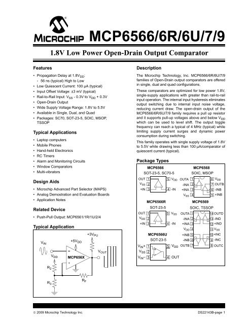
MCP6566/6R/6U/7/9<br />
<strong>1.8V</strong> <strong>Low</strong> <strong>Power</strong> <strong>Open</strong>-<strong>Drain</strong> <strong>Output</strong> <strong>Comparator</strong><br />
Features<br />
• Propagation Delay at <strong>1.8V</strong> DD :<br />
- 56 ns (typical) High to <strong>Low</strong><br />
• <strong>Low</strong> Quiescent Current: 100 µA (typical)<br />
• Input Offset Voltage: ±3 mV (typical)<br />
• Rail-to-Rail Input: V SS - 0.3V to V DD + 0.3V<br />
• <strong>Open</strong>-<strong>Drain</strong> <strong>Output</strong><br />
• Wide Supply Voltage Range: <strong>1.8V</strong> to 5.5V<br />
• Available in Single, Dual, and Quad<br />
• Packages: SC70, SOT-23-5, SOIC, MSOP,<br />
TSSOP<br />
Typical Applications<br />
• Laptop computers<br />
• Mobile Phones<br />
• Hand-held Electronics<br />
• RC Timers<br />
• Alarm and Monitoring Circuits<br />
• Window <strong>Comparator</strong>s<br />
• Multi-vibrators<br />
Design Aids<br />
• <strong>Microchip</strong> Advanced Part Selector (MAPS)<br />
• Analog Demostration and Evaluation Boards<br />
• Application Notes<br />
Related Device<br />
• Push-Pull <strong>Output</strong>: MCP6561/1R/1U/2/4<br />
Typical Application<br />
V IN<br />
V DD<br />
R 2<br />
R 3<br />
+5V DD<br />
MCP656X<br />
R F<br />
+3V PU<br />
V OUT<br />
Description<br />
The <strong>Microchip</strong> Technology, Inc. MCP6566/6R/6U/7/9<br />
families of <strong>Open</strong>-<strong>Drain</strong> output comparators are offered<br />
in single, dual and quad configurations.<br />
These comparators are optimized for low power <strong>1.8V</strong>,<br />
single-supply applications with greater than rail-to-rail<br />
input operation. The internal input hysteresis eliminates<br />
output switching due to internal input noise voltage,<br />
reducing current draw. The open-drain output of the<br />
MCP6566/6R/6U/7/9 family requires a pull up resistor<br />
and it supports pull-up voltages above and below V DD<br />
which can be used to level shift. The output toggle<br />
frequency can reach a typical of 4 MHz (typical) while<br />
limiting supply current surges and dynamic power<br />
consumption during switching.<br />
This family operates with single supply voltage of <strong>1.8V</strong><br />
to 5.5V while drawing less than 100 µA/comparator of<br />
quiescent current (typical).<br />
Package Types<br />
MCP6566<br />
SOT-23-5, SC70-5<br />
OUT<br />
V SS<br />
+IN<br />
1<br />
2<br />
3<br />
5<br />
4<br />
V DD<br />
-IN<br />
+<br />
+<br />
-<br />
-<br />
OUTA 1<br />
-INA 2<br />
+INA 3<br />
V SS 4<br />
MCP6568<br />
SOIC, MSOP<br />
-<br />
+<br />
+ -<br />
8<br />
V DD<br />
7 OUTB<br />
6 -INB<br />
5 +INB<br />
MCP6566R<br />
SOT-23-5<br />
MCP6569<br />
SOIC, TSSOP<br />
OUT 1<br />
5 V SS OUTA 1<br />
14 OUTD<br />
V DD 2<br />
-INA 2 - + + - 13 -IND<br />
+IN 3<br />
4 -IN +INA 3<br />
12 +IND<br />
V DD 4<br />
11 V SS<br />
MCP6566U +INB 5<br />
10 +INC<br />
SOT-23-5<br />
-INB 6<br />
- + + -<br />
9 -INC<br />
V IN + 1 5 V DD OUTB 7<br />
8 OUTC<br />
V SS 2<br />
V IN – 3 4 OUT<br />
+<br />
-<br />
© 2009 <strong>Microchip</strong> Technology Inc. DS22143B-page 1
MCP6566/6R/6U/7/9<br />
NOTES:<br />
DS22143B-page 2<br />
© 2009 <strong>Microchip</strong> Technology Inc.
MCP6566/6R/6U/7/9<br />
1.0 ELECTRICAL<br />
CHARACTERISTICS<br />
1.1 Maximum Ratings*<br />
V DD - V SS ....................................................................... 6.5V<br />
<strong>Open</strong>-<strong>Drain</strong> <strong>Output</strong>.............................................V SS + 10.5V<br />
All other inputs and outputs...........V SS – 0.3V to V DD + 0.3V<br />
Difference Input voltage ......................................|V DD - V SS |<br />
<strong>Output</strong> Short Circuit Current .................................... ±25 mA<br />
Current at Input Pins .................................................. ±2 mA<br />
Current at <strong>Output</strong> and Supply Pins .......................... ±50 mA<br />
Storage temperature ................................... -65°C to +150°C<br />
Ambient temp. with power applied .............. -40°C to +125°C<br />
Junction temp............................................................ +150°C<br />
DC CHARACTERISTICS<br />
ESD protection on all pins (HBM/MM) .................≥ 4 kV/300V<br />
*Notice: Stresses above those listed under “Maximum<br />
Ratings” may cause permanent damage to the device. This is<br />
a stress rating only and functional operation of the device at<br />
those or any other conditions above those indicated in the<br />
operational listings of this specification is not implied. Exposure<br />
to maximum rating conditions for extended periods may<br />
affect device reliability.<br />
Electrical Characteristics: Unless otherwise indicated: V DD = +<strong>1.8V</strong> to +5.5V, V SS = GND, T A = +25°C, V IN + = V DD /2, V IN - = V SS ,<br />
and R Pull-Up = 20 kΩ to V PU = V DD (see Figure 1-1).<br />
Parameters Symbol Min Typ Max Units Conditions<br />
<strong>Power</strong> Supply<br />
Supply Voltage V DD 1.8 — 5.5 V<br />
Quiescent Current per comparator I Q 60 100 130 µA I OUT = 0<br />
<strong>Power</strong> Supply Rejection Ratio PSRR 63 70 — dB V CM = V SS<br />
Input<br />
Input Offset Voltage V OS -10 ±3 +10 mV V CM = V SS (Note 1)<br />
Input Offset Drift ΔV OS /ΔT — ±2 — µV/°C V CM = V SS<br />
Input Offset Current I OS — ±1 — pA V CM = V SS<br />
Input Bias Current I B — 1 — pA T A = +25°C, V IN - = V DD /2<br />
— 60 — pA T A = +85°C, V IN - = V DD /2<br />
— 1500 5000 pA T A = +125°C, V IN - = V DD /2<br />
Input Hysteresis Voltage V HYST 1.0 — 5.0 mV V CM = V SS (Notes 1, 2)<br />
Input Hysteresis Linear Temp. Co. TC 1 — 10 — µV/°C<br />
Input Hysteresis Quadratic Temp. Co. TC 2 — 0.3 — µV/°C 2<br />
Common-Mode Input Voltage Range V CMR V SS −0.2 — V DD +0.2 V V DD = <strong>1.8V</strong><br />
V SS −0.3 — V DD +0.3 V V DD = 5.5V<br />
Common-Mode Rejection Ratio CMRR 54 66 — dB V CM = -0.3V to V DD +0.3V, V DD = 5.5V<br />
50 63 — dB V CM = V DD /2 to V DD +0.3V, V DD = 5.5V<br />
54 65 — dB V CM = -0.3V to V DD /2, V DD = 5.5V<br />
Common Mode Input Impedance Z CM — 10 13 ||4 — Ω||pF<br />
Differential Input Impedance Z DIFF — 10 13 ||2 — Ω||pF<br />
Note 1: The input offset voltage is the center of the input-referred trip points. The input hysteresis is the difference between the<br />
input-referred trip points.<br />
2: V HYST at different temperatures is estimated using V HYST (T A ) = V HYST @ +25°C + (T A - 25°C) TC 1 + (T A - 25°C) 2 TC 2 .<br />
3: Limit the output current to Absolute Maximum Rating of 50 mA.<br />
4: The pull up voltage for the open drain output V PULL_UP can be as high as the absolute maximum rating of 10.5V. In this<br />
case, I OH_leak can be higher than 1 µA (see Figure 2-30).<br />
© 2009 <strong>Microchip</strong> Technology Inc. DS22143B-page 3
MCP6566/6R/6U/7/9<br />
DC CHARACTERISTICS (CONTINUED)<br />
Electrical Characteristics: Unless otherwise indicated: V DD = +<strong>1.8V</strong> to +5.5V, V SS = GND, T A = +25°C, V IN + = V DD /2, V IN - = V SS ,<br />
and R Pull-Up = 20 kΩ to V PU = V DD (see Figure 1-1).<br />
Parameters Symbol Min Typ Max Units Conditions<br />
Push-Pull <strong>Output</strong><br />
Pull-up Voltage V PULL_UP 1.6 — 5.5 V<br />
High Level <strong>Output</strong> Voltage V OH — — V PULL_UP V (see Figure 1-1) (Notes 3, 4)<br />
High Level <strong>Output</strong> Current leakage I OH_leak — — 1 µA Note 4<br />
<strong>Low</strong> Level <strong>Output</strong> Voltage V OL — — 0.6 V I OUT = 3mA/8mA @ V DD = <strong>1.8V</strong>/5.5V<br />
Short Circuit Current (Notes 3) I SC — ±30 — mA Not to exceed Absolute Max. Rating<br />
<strong>Output</strong> Pin Capacitance C OUT — 8 — pF<br />
Note 1: The input offset voltage is the center of the input-referred trip points. The input hysteresis is the difference between the<br />
input-referred trip points.<br />
2: V HYST at different temperatures is estimated using V HYST (T A ) = V HYST @ +25°C + (T A - 25°C) TC 1 + (T A - 25°C) 2 TC 2 .<br />
3: Limit the output current to Absolute Maximum Rating of 50 mA.<br />
4: The pull up voltage for the open drain output V PULL_UP can be as high as the absolute maximum rating of 10.5V. In this<br />
case, I OH_leak can be higher than 1 µA (see Figure 2-30).<br />
AC CHARACTERISTICS<br />
Electrical Characteristics: Unless otherwise indicated,: Unless otherwise indicated,: V DD = +<strong>1.8V</strong> to +5.5V, V SS = GND,<br />
T A = +25°C, V IN+ = V DD /2, V IN- = V SS , R Pull-Up = 20 kΩ to V PU = V DD , and C L = 25 pf (see Figure 1-1).<br />
Parameters<br />
Symbo<br />
l<br />
Min Typ Max Units Conditions<br />
Propagation Delay<br />
High-to-<strong>Low</strong>,100 mV Overdrive t PHL — 56 80 ns V CM = V DD /2, V DD = <strong>1.8V</strong><br />
— 34 80 ns V CM = V DD /2, V DD = 5.5V<br />
<strong>Output</strong><br />
Fall Time t F — 20 — ns<br />
Maximum Toggle Frequency f TG — 4 — MHz V DD = 5.5V<br />
— 2 — MHz V DD = <strong>1.8V</strong><br />
Input Voltage Noise E NI — 350 — µV P-P 10 Hz to 10 MHz (Note 1)<br />
Note 1: ENI is based on SPICE simulation.<br />
2: Rise time t R and t PLH depend on the load (R L and C L ). These specification are valid for the specified load only.<br />
TEMPERATURE SPECIFICATIONS<br />
Electrical Characteristics: Unless otherwise indicated: V DD = +<strong>1.8V</strong> to +5.5V and V SS = GND.<br />
Parameters<br />
Symbo<br />
l<br />
Min Typ Max Units Conditions<br />
Temperature Ranges<br />
Specified Temperature Range T A -40 — +125 °C<br />
Operating Temperature Range T A -40 — +125 °C<br />
Storage Temperature Range T A -65 — +150 °C<br />
Thermal Package Resistances<br />
Thermal Resistance, SC70-5 θ JA — 331 — °C/W<br />
Thermal Resistance, SOT-23-5 θ JA — 220.7 — °C/W<br />
Thermal Resistance, 8L-MSOP θ JA — 211 — °C/W<br />
Thermal Resistance, 8L-SOIC θ JA — 149.5 — °C/W<br />
Thermal Resistance, 14L-SOIC θ JA — 95.3 — °C/W<br />
Thermal Resistance, 14L-TSSOP θ JA — 100 — °C/W<br />
DS22143B-page 4<br />
© 2009 <strong>Microchip</strong> Technology Inc.
MCP6566/6R/6U/7/9<br />
1.2 Test Circuit Configuration<br />
This test circuit configuration is used to determine the<br />
AC and DC specifications.<br />
V DD<br />
V SS = 0V<br />
MCP656X<br />
V PU = V DD<br />
200 kΩ<br />
200 kΩ<br />
I OUT<br />
R PU<br />
20 kΩ<br />
V OUT<br />
25 pF<br />
V IN = V SS<br />
FIGURE 1-1: AC and DC Test Circuit for<br />
the <strong>Open</strong>-<strong>Drain</strong> <strong>Output</strong> <strong>Comparator</strong>s.<br />
© 2009 <strong>Microchip</strong> Technology Inc. DS22143B-page 5
MCP6566/6R/6U/7/9<br />
NOTES:<br />
DS22143B-page 6<br />
© 2009 <strong>Microchip</strong> Technology Inc.
MCP6566/6R/6U/7/9<br />
2.0 TYPICAL PERFORMANCE CURVES<br />
Note:<br />
The graphs and tables provided following this note are a statistical summary based on a limited number of<br />
samples and are provided for informational purposes only. The performance characteristics listed herein<br />
are not tested or guaranteed. In some graphs or tables, the data presented may be outside the specified<br />
operating range (e.g., outside specified power supply range) and therefore outside the warranted range.<br />
Note: Unless otherwise indicated, V DD = +<strong>1.8V</strong> to +5.5V, V SS = GND, T A = +25°C, V IN + = V DD /2, V IN – = GND,<br />
R L = 20 kΩ to V PU = V DD , and C L = 25 pF.<br />
Occurrences (%)<br />
50%<br />
40%<br />
30%<br />
20%<br />
10%<br />
VDD = <strong>1.8V</strong><br />
V CM = V SS<br />
Avg. = -0.1 mV<br />
StDev = 2.1 mV<br />
3588 units<br />
V DD = 5.5V<br />
V CM = V SS<br />
Avg. = -0.9 mV<br />
StDev = 2.1 mV<br />
3588 units<br />
Occurrences (%)<br />
30%<br />
25%<br />
20%<br />
15%<br />
10%<br />
5%<br />
V DD = <strong>1.8V</strong><br />
Avg. = 3.4 mV<br />
StDev = 0.2 mV<br />
3588 units<br />
V DD = 5.5V<br />
Avg. = 3.6 mV<br />
StDev = 0.1 mV<br />
3588 units<br />
0%<br />
-10 -8 -6 -4 -2 0 2 4 6 8 10<br />
V OS (mV)<br />
0%<br />
1.0 1.5 2.0 2.5 3.0 3.5 4.0 4.5 5.0<br />
V HYST (mV)<br />
FIGURE 2-1:<br />
Input Offset Voltage.<br />
FIGURE 2-4:<br />
Input Hysteresis Voltage.<br />
Occurrences (%)<br />
60%<br />
50%<br />
40%<br />
30%<br />
20%<br />
10%<br />
0%<br />
V CM = V SS<br />
Avg. = 0.9 µV/°C<br />
StDev = 6.6 µV/°C<br />
1380 Units<br />
T A = -40°C to +125°C<br />
-60 -48 -36 -24 -12 0 12 24 36 48 60<br />
V OS Drift (µV/°C)<br />
Occurrences (%)<br />
60%<br />
50%<br />
40%<br />
30%<br />
20%<br />
10%<br />
0%<br />
V DD = 5.5V<br />
Avg. = 10.4 µV/°C<br />
StDev = 0.6 µV/°C<br />
1380 Units<br />
T A = -40°C to 125°C<br />
V CM = V SS<br />
V DD = <strong>1.8V</strong><br />
Avg. = 12 µV/°C<br />
StDev = 0.6 µV/°C<br />
0 2 4 6 8 10 12 14 16 18 20<br />
V HYST Drift, TC1 (µV/°C)<br />
FIGURE 2-2:<br />
Input Offset Voltage Drift.<br />
FIGURE 2-5: Input Hysteresis Voltage<br />
Drift - Linear Temp. Co. (TC1).<br />
V OUT (V)<br />
7.0<br />
6.0<br />
5.0<br />
4.0<br />
3.0<br />
2.0<br />
1.0<br />
VDD = 5.5V<br />
V IN -<br />
V OUT<br />
VIN+ = VDD/2<br />
Occurrences (%)<br />
30%<br />
20%<br />
10%<br />
V DD = <strong>1.8V</strong><br />
VDD = 5.5V<br />
StDev = 0.1 µV/°C 2 StDev = 0.2 µV/°C 2<br />
Avg. = 0.25 µV/°C 2<br />
Avg. = 0.3 µV/°C 2<br />
1380 Units<br />
T A = -40°C to +125°C<br />
V CM = V SS<br />
0.0<br />
-1.0<br />
Time (3 µs/div)<br />
0%<br />
-0.50 -0.25 0.00 0.25 0.50 0.75 1.00<br />
V HYST Drift, TC2 (µV/°C 2 )<br />
FIGURE 2-3:<br />
Phase Reversal.<br />
Input vs. <strong>Output</strong> Signal, No<br />
FIGURE 2-6: Input Hysteresis Voltage<br />
Drift - Quadratic Temp. Co. (TC2).<br />
© 2009 <strong>Microchip</strong> Technology Inc. DS22143B-page 7
MCP6566/6R/6U/7/9<br />
Note: Unless otherwise indicated, V DD = +<strong>1.8V</strong> to +5.5V, V SS = GND, T A = +25°C, V IN + = V DD /2, V IN – = GND,<br />
R L = 20 kΩ to V PU = V DD , and C L = 25 pF.<br />
3.0<br />
5.0<br />
V OS (mV)<br />
2.0<br />
1.0<br />
0.0<br />
-1.0<br />
-2.0<br />
V DD = <strong>1.8V</strong><br />
V DD = 5.5V<br />
V CM = V SS<br />
V HYST (mV)<br />
4.0<br />
3.0<br />
2.0<br />
V CM = V SS<br />
V DD = 5.0V<br />
VDD= <strong>1.8V</strong><br />
-3.0<br />
-50 -25 0 25 50 75 100 125<br />
Temperature (°C)<br />
1.0<br />
-50 -25 0 25 50 75 100 125<br />
Temperature (°C)<br />
FIGURE 2-7:<br />
Temperature.<br />
Input Offset Voltage vs.<br />
FIGURE 2-10:<br />
Temperature.<br />
Input Hysteresis Voltage vs.<br />
V OS (mV)<br />
4.0<br />
2.0<br />
0.0<br />
-2.0<br />
V DD = <strong>1.8V</strong><br />
TA= +125°C<br />
TA= +85°C<br />
TA= +25°C<br />
T A = -40°C<br />
-4.0<br />
-0.3 0.0 0.3 0.6 0.9 1.2 1.5 1.8 2.1<br />
V CM (V)<br />
FIGURE 2-8: Input Offset Voltage vs.<br />
Common-mode Input Voltage.<br />
V HYST (mV)<br />
5.0<br />
4.0<br />
3.0<br />
T A = +125°C<br />
2.0<br />
TA= +25°C<br />
TA= +85°C<br />
V DD = <strong>1.8V</strong><br />
TA= -40°C<br />
1.0<br />
-0.3 0.0 0.3 0.6 0.9 1.2 1.5 1.8 2.1<br />
V CM (V)<br />
FIGURE 2-11: Input Hysteresis Voltage vs.<br />
Common-mode Input Voltage.<br />
V OS (mV)<br />
3.0<br />
2.0<br />
1.0<br />
0.0<br />
-1.0<br />
V DD = 5.5V<br />
TA= -40°C<br />
T A = +25°C<br />
-2.0<br />
T A = +85°C<br />
T A = +125°C<br />
-3.0<br />
-1.0 0.0 1.0 2.0 3.0 4.0 5.0 6.0<br />
V CM (V)<br />
FIGURE 2-9: Input Offset Voltage vs.<br />
Common-mode Input Voltage.<br />
V HYST (mV)<br />
5.0<br />
4.0<br />
3.0<br />
T A = -40°C<br />
2.0<br />
T A = +25°C<br />
T A = +85°C<br />
T A = +125°C<br />
VDD = 5.5V<br />
1.0<br />
-0.5 0.5 1.5 2.5 3.5 4.5 5.5<br />
V CM (V)<br />
FIGURE 2-12: Input Hysteresis Voltage vs.<br />
Common-mode Input Voltage.<br />
DS22143B-page 8<br />
© 2009 <strong>Microchip</strong> Technology Inc.
MCP6566/6R/6U/7/9<br />
Note: Unless otherwise indicated, V DD = +<strong>1.8V</strong> to +5.5V, V SS = GND, T A = +25°C, V IN + = V DD /2, V IN – = GND,<br />
R L = 20 kΩ to V PU = V DD , and C L = 25 pF.<br />
V OS (mV)<br />
3.0<br />
2.0<br />
1.0<br />
0.0<br />
-1.0<br />
-2.0<br />
TA= -40°C<br />
T A = +25°C<br />
T A = +85°C<br />
T A = +125°C<br />
V HYST (mV)<br />
5.0<br />
4.0<br />
3.0<br />
2.0<br />
T A = +125°C<br />
T A = +85°C<br />
T A = +25°C<br />
T A = -40°C<br />
-3.0<br />
1.5 2.5 3.5 4.5 5.5<br />
V DD (V)<br />
FIGURE 2-13: Input Offset Voltage vs.<br />
Supply Voltage vs. Temperature.<br />
1.0<br />
1.5 2.5 3.5 4.5 5.5<br />
V DD (V)<br />
FIGURE 2-16: Input Hysteresis Voltage vs.<br />
Supply Voltage vs. Temperature.<br />
50%<br />
140.0<br />
Occurrences (%)<br />
40%<br />
30%<br />
20%<br />
10%<br />
VDD = <strong>1.8V</strong><br />
Avg. = 88 µA<br />
StDev= 4 µA<br />
1794 units<br />
VDD = 5.5V<br />
Avg. = 97 µA<br />
StDev= 4 µA<br />
1794 units<br />
I Q (µA)<br />
120.0<br />
100.0<br />
80.0<br />
60.0<br />
40.0<br />
20.0<br />
TA= -40°C<br />
TA= +25°C<br />
TA= +85°C<br />
TA= +125°C<br />
0%<br />
60 70 80 90 100 110 120 130<br />
I Q (µA)<br />
0.0<br />
0.0 1.0 2.0 3.0 4.0 5.0 6.0<br />
V DD (V)<br />
FIGURE 2-14:<br />
Quiescent Current.<br />
FIGURE 2-17: Quiescent Current vs.<br />
Supply Voltage vs Temperature.<br />
I Q (µA)<br />
130<br />
120<br />
110<br />
100<br />
90<br />
80<br />
70<br />
V DD = <strong>1.8V</strong><br />
Sweep VIN+ ,VIN- - = VDD/2V Sweep VIN- ,VIN+ = VDD/2<br />
V /2<br />
60<br />
-0.5 0.0 0.5 1.0 1.5 2.0 2.5<br />
V CM (V)<br />
FIGURE 2-15: Quiescent Current vs.<br />
Common-mode Input Voltage.<br />
I Q (µA)<br />
130<br />
120<br />
110<br />
100<br />
90<br />
80<br />
70<br />
V DD = 5.5V<br />
Sweep V IN+ ,V IN - = V DD /2<br />
Sweep VIN- ,VIN+ = VDD/2<br />
60<br />
-1.0 0.0 1.0 2.0 3.0 4.0 5.0 6.0<br />
V CM (V)<br />
FIGURE 2-18: Quiescent Current vs.<br />
Common-mode Input Voltage.<br />
© 2009 <strong>Microchip</strong> Technology Inc. DS22143B-page 9
MCP6566/6R/6U/7/9<br />
Note: Unless otherwise indicated, V DD = +<strong>1.8V</strong> to +5.5V, V SS = GND, T A = +25°C, V IN + = V DD /2, V IN – = GND,<br />
R L = 20 kΩ to V PU = V DD , and C L = 25 pF.<br />
150<br />
IDD Spike near VPU = 0.9V<br />
150<br />
VDD = 5.5 V<br />
125<br />
V DD = 5.5V<br />
V DD = 4.5V<br />
VDD = 3.5V<br />
125<br />
V DD = 4.5 V<br />
V DD = 3.5 V<br />
I Q (µA)<br />
100<br />
I Q (µA)<br />
100<br />
75<br />
50<br />
VDD = 2.5V<br />
VDD = 2.0V<br />
VDD = <strong>1.8V</strong><br />
0.5 1.5 2.5 3.5 4.5 5.5 6.5 7.5 8.5 9.5 10.5<br />
V PU (V)<br />
75<br />
VDD = 2.5 V<br />
VDD = 2.0 V<br />
V DD = 1.8 V<br />
50<br />
-4.5 -2.5 -0.5 1.5 3.5 5.5 7.5 9.5<br />
V PU - V DD (V)<br />
FIGURE 2-19:<br />
Pull-up Voltage.<br />
Quiescent Current vs.<br />
FIGURE 2-22: Quiescent Current vs.<br />
Pull-up to Supply Voltage Difference.<br />
IQ (µA)<br />
400<br />
350<br />
300<br />
250<br />
200<br />
150<br />
100<br />
100 mV Over-Drive<br />
V CM = V DD /2<br />
R L = <strong>Open</strong><br />
0dB <strong>Output</strong> Attenuation<br />
VDD = <strong>1.8V</strong><br />
VDD = 5.5V<br />
50<br />
10 100 1000 1k 10000 10k 100000 100k 100000 1M 1E+07 10M<br />
Toggle Frequency (Hz) 0<br />
I OH_leak (pA)<br />
100,000<br />
10,000<br />
1,000<br />
100<br />
10<br />
1<br />
T A =<br />
T A = +85°C<br />
T A = +25°C<br />
1.5 2.5 3.5 4.5 5.5 6.5 7.5 8.5 9.5 10.5<br />
V PU (V)<br />
FIGURE 2-20:<br />
Toggle Frequency.<br />
Quiescent Current vs.<br />
FIGURE 2-23:<br />
Pull-up Voltage.<br />
<strong>Output</strong> Leakage Current vs.<br />
1000<br />
V DD = <strong>1.8V</strong><br />
1000<br />
V DD = 5.5V<br />
V OL (mV)<br />
800<br />
600<br />
400<br />
200<br />
TA = +125°C<br />
T A = +85°C<br />
T A = +25°C<br />
T A = -40°C<br />
V OL (mV)<br />
800<br />
600<br />
400<br />
200<br />
TA = +125°C<br />
T A = +85°C<br />
TA = +25°C<br />
T A = -40°C<br />
0<br />
0.0 3.0 6.0 9.0 12.0 15.0<br />
I OUT (mA)<br />
0<br />
0 5 10 15 20 25<br />
I OUT (mA)<br />
FIGURE 2-21:<br />
Current.<br />
<strong>Output</strong> Headroom vs <strong>Output</strong><br />
FIGURE 2-24:<br />
Current.<br />
<strong>Output</strong> Headroom Vs <strong>Output</strong><br />
DS22143B-page 10<br />
© 2009 <strong>Microchip</strong> Technology Inc.
MCP6566/6R/6U/7/9<br />
Note: Unless otherwise indicated, V DD = +<strong>1.8V</strong> to +5.5V, V SS = GND, T A = +25°C, V IN + = V DD /2, V IN – = GND,<br />
R L = 20 kΩ to V PU = V DD , and C L = 25 pF.<br />
Occurrences (%)<br />
50%<br />
40%<br />
30%<br />
20%<br />
10%<br />
VDD= <strong>1.8V</strong><br />
100 mV Over-Drive<br />
V CM = V DD /2<br />
t PHL<br />
Avg. = 54.4 ns<br />
StDev= 2 ns<br />
198 units<br />
Occurrences (%)<br />
50%<br />
40%<br />
30%<br />
20%<br />
10%<br />
t PHL<br />
Avg. = 33 ns<br />
StDev= 1 ns<br />
198 units<br />
V DD = 5.5V<br />
100mV Over-Drive<br />
V CM = V DD /2<br />
0%<br />
30 35 40 45 50 55 60 65 70 75 80<br />
Prop. Delay (ns)<br />
0%<br />
30 35 40 45 50 55 60 65 70 75 80<br />
Prop. Delay (ns)<br />
FIGURE 2-25:<br />
Delays.<br />
High-to-<strong>Low</strong> Propagation<br />
FIGURE 2-28: High-to-<strong>Low</strong> Propagation<br />
Delays.<br />
Prop. Delay (ns)<br />
260<br />
V CM = V DD /2<br />
210<br />
160<br />
t PHL , V DD = <strong>1.8V</strong><br />
110<br />
tPHL , VDD = 5.5V<br />
60<br />
10<br />
1 10 100 1000<br />
Over-Drive (mV)<br />
Prop. Delay (ns)<br />
80<br />
70<br />
60<br />
50<br />
40<br />
30<br />
20<br />
100 mV Over-Drive<br />
V CM = V DD /2<br />
tPHL , VDD = <strong>1.8V</strong><br />
tPHL , VDD = 5.5V<br />
-50 -25 0 25 50 75 100 125<br />
Temperature (°C)<br />
FIGURE 2-26:<br />
Over-Drive.<br />
Propagation Delay vs. Input<br />
FIGURE 2-29:<br />
Temperature.<br />
Propagation Delay vs.<br />
Prop. Delay (ns)<br />
140<br />
120<br />
100<br />
80<br />
60<br />
40<br />
20<br />
t PHL , 10 mV Over-Drive<br />
tPHL , 100 mV Over-Drive<br />
VCM = VDD/2<br />
1.5 2.5 3.5 4.5 5.5<br />
V DD (V)<br />
I SC (mA)<br />
120<br />
80<br />
40<br />
0<br />
-40<br />
-80<br />
-120<br />
TA= -40°C<br />
TA= +25°C<br />
T A = +85°C<br />
T A = +125°C<br />
TA= -40°C<br />
T A = +25°C<br />
T A = +85°C<br />
TA= +125°C<br />
0.0 1.0 2.0 3.0 4.0 5.0 6.0<br />
V DD (V)<br />
FIGURE 2-27:<br />
Supply Voltage.<br />
Propagation Delay vs.<br />
FIGURE 2-30: Short Circuit Current vs.<br />
Supply Voltage vs. Temperature.<br />
© 2009 <strong>Microchip</strong> Technology Inc. DS22143B-page 11
MCP6566/6R/6U/7/9<br />
Note: Unless otherwise indicated, V DD = +<strong>1.8V</strong> to +5.5V, V SS = GND, T A = +25°C, V IN + = V DD /2, V IN – = GND,<br />
R L = 20 kΩ to V PU = V DD , and C L = 25 pF.<br />
80<br />
80<br />
Prop. Delay (ns)<br />
70<br />
60<br />
50<br />
40<br />
30<br />
VDD= <strong>1.8V</strong><br />
100 mV Over-Drive<br />
tPHL<br />
Prop. Delay (ns)<br />
70<br />
60<br />
50<br />
40<br />
30<br />
V DD = 5.5V<br />
100 mV Over-Drive<br />
t PHL<br />
20<br />
0.00 0.50 1.00 1.50 2.00<br />
V CM (V)<br />
FIGURE 2-31: Propagation Delay vs.<br />
Common-mode Input Voltage.<br />
20<br />
0.0 1.0 2.0 3.0 4.0 5.0 6.0<br />
V CM (V)<br />
FIGURE 2-34: Propagation Delay vs.<br />
Common-mode Input Voltage.<br />
Prop. Delay (µs)<br />
1000<br />
100<br />
10<br />
1<br />
0.1<br />
100mV Over-Drive<br />
V CM = V DD /2<br />
VDD = 5.5V, tPHL<br />
VDD = <strong>1.8V</strong>, tPHL<br />
Prop. Delay (ns)<br />
10000<br />
1000<br />
100<br />
100 mV Over-Drive<br />
V CM = V DD /2<br />
t PLH<br />
t PHL<br />
0.01<br />
0.001 1 0.01 10 0.1 100 1000 1 10000 100000 1E+06 1000<br />
Capacitive Load (nf)<br />
10<br />
0.1 1.0 10.0 100.0<br />
R PU (kΩ)<br />
FIGURE 2-32:<br />
Capacitive Load.<br />
Propagation Delay vs.<br />
FIGURE 2-35:<br />
Pull-up Resistor.<br />
Propagation Delay vs.<br />
Input Current (A)<br />
1E+11 10m<br />
1E+09 1m<br />
1E+07 10µ<br />
1E+05 100n<br />
1E+03 1n<br />
1E+01 10p<br />
T A = -40°C<br />
TA= +25°C<br />
T A = +85°C<br />
TA= +125°C<br />
1E-01 0.1p<br />
-0.8 -0.6 -0.4 -0.2 0<br />
Input Voltage (V)<br />
Prop. Delay (ns)<br />
10000<br />
1000<br />
100<br />
10<br />
100 mV Over-Drive<br />
VCM = VDD/2<br />
tPLH, VDD = <strong>1.8V</strong><br />
t PLH, V DD = 5.5V<br />
t PHL, V DD = <strong>1.8V</strong><br />
t PLH, V DD = 5.5V<br />
0.0 0.5 1.0 1.5 2.0 2.5 3.0 3.5 4.0 4.5 5.0 5.5<br />
V PU (V)<br />
FIGURE 2-33: Input Bias Current vs. Input<br />
Voltage vs Temperature.<br />
FIGURE 2-36:<br />
Pull-up Voltage.<br />
Propagation Delay vs.<br />
DS22143B-page 12<br />
© 2009 <strong>Microchip</strong> Technology Inc.
MCP6566/6R/6U/7/9<br />
Note: Unless otherwise indicated, V DD = +<strong>1.8V</strong> to +5.5V, V SS = GND, T A = +25°C, V IN + = V DD /2, V IN – = GND,<br />
R L = 20 kΩ to V PU = V DD , and C L = 25 pF.<br />
CMRR/PSRR (dB)<br />
80<br />
78<br />
76<br />
74<br />
72<br />
70<br />
Input Referred<br />
PSRR<br />
CMRR<br />
V CM = V SS<br />
V DD = <strong>1.8V</strong> to 5.5V<br />
VCM = -0.3V to VDD + 0.3V<br />
V DD = 5.5V<br />
-50 -25 0 25 50 75 100 125<br />
Temperature (°C)<br />
Occurrences (%)<br />
30%<br />
20%<br />
10%<br />
VCM = VDD/2 to VDD+ 0.2V<br />
Avg. = 0.7 mV<br />
StDev= 1 mV<br />
VCM = -0.2V to VDD/2<br />
Avg. = 0.5 mV<br />
StDev= 0.1 mV<br />
V CM = -0.2V to V DD + 0.2V<br />
Avg. = 0.6 mV<br />
StDev= 0.1 mV<br />
V DD = <strong>1.8V</strong><br />
3588 units<br />
0%<br />
-5 -4 -3 -2 -1 0 1 2 3 4 5<br />
CMRR (mV/V)<br />
FIGURE 2-37: Common-mode Rejection<br />
Ratio and <strong>Power</strong> Supply Rejection Ratio vs.<br />
Temperature.<br />
FIGURE 2-40:<br />
Ratio (CMRR).<br />
Common-mode Rejection<br />
Occurrences (%)<br />
30%<br />
25%<br />
20%<br />
15%<br />
10%<br />
5%<br />
V CM = V SS<br />
Avg. = 200 µV/V<br />
StDev= 94 µV/V<br />
3588 units<br />
Occurrences (%)<br />
30%<br />
20%<br />
10%<br />
VCM = VDD/2 to VDD+ 0.3V<br />
Avg. = 0.03 mV<br />
StDev= 0.7 mV<br />
VCM = -0.3V to VDD/2<br />
Avg. = 0.2 mV<br />
StDev= 0.4 mV<br />
V CM = -0.3V to V DD + 0.3V<br />
Avg. = 0.1 mV<br />
StDev= 0.4 mV<br />
V DD = 5.5V<br />
3588 units<br />
0%<br />
-600 -400 -200 0 200 400 600<br />
PSRR (µV/V)<br />
0%<br />
-2.5 -2.0 -1.5 -1.0 -0.5 0.0 0.5 1.0 1.5 2.0 2.5<br />
CMRR (mV/V)<br />
FIGURE 2-38:<br />
Ratio (PSRR).<br />
<strong>Power</strong> Supply Rejection<br />
FIGURE 2-41:<br />
Ratio (CMRR).<br />
Common-mode Rejection<br />
I OS and I B (pA)<br />
1000<br />
100<br />
10<br />
1<br />
0.1<br />
I B<br />
|I OS |<br />
25 50 75 100 125<br />
Temperature (°C)<br />
FIGURE 2-39: Input Offset Current and<br />
Input Bias Current vs. Temperature.<br />
I OS and I B (pA)<br />
10000<br />
1000<br />
100<br />
10<br />
1<br />
0.1<br />
0.01<br />
0.001<br />
I B @ T A = +125°C<br />
I B @ T A = +85°C<br />
|I OS| @ T A = +125°C<br />
|I OS |@ T A = +85°C<br />
V DD = 5.5V<br />
0 1 2 3 4 5 6<br />
V CM (V)<br />
FIGURE 2-42: Input Offset Current and<br />
Input Bias Current vs. Common-mode Input<br />
Voltage vs. Temperature.<br />
© 2009 <strong>Microchip</strong> Technology Inc. DS22143B-page 13
MCP6566/6R/6U/7/9<br />
Note: Unless otherwise indicated, V DD = +<strong>1.8V</strong> to +5.5V, V SS = GND, T A = +25°C, V IN + = V DD /2, V IN – = GND,<br />
R L = 20 kΩ to V PU = V DD , and C L = 25 pF.<br />
<strong>Output</strong> Jitter pk-pk (ns)<br />
10000<br />
1000<br />
100<br />
10<br />
1<br />
V DD = 5.5V<br />
VIN+ = 2Vpp (sine)<br />
0.1<br />
100 1000 1k 10000 10k 100000 100k 100000 1M 1E+07 10M<br />
Input Frequency (Hz) 0<br />
FIGURE 2-43:<br />
Frequency.<br />
<strong>Output</strong> Jitter vs. Input<br />
DS22143B-page 14<br />
© 2009 <strong>Microchip</strong> Technology Inc.
MCP6566/6R/6U/7/9<br />
3.0 PIN DESCRIPTIONS<br />
Descriptions of the pins are listed in Table 3-1.<br />
TABLE 3-1: PIN FUNCTION TABLE<br />
MCP6566 MCP6566R MCP6566U MCP6568 MCP6569<br />
SC70-5,<br />
SOT-23-5<br />
SOT-23-5<br />
SOT-23-5<br />
MSOP,<br />
SOIC<br />
SOIC,<br />
TSSOP<br />
Symbol<br />
Description<br />
1 1 5 1 1 OUT, OUTA Digital <strong>Output</strong> (comparator A)<br />
4 4 3 2 2 V IN –, V INA – Inverting Input (comparator A)<br />
3 3 1 3 3 V IN +, V INA + Non-inverting Input (comparator A)<br />
5 2 4 8 4 V DD Positive <strong>Power</strong> Supply<br />
— — — 5 5 V INB + Non-inverting Input (comparator B)<br />
— — — 6 6 V INB – Inverting Input (comparator B)<br />
— — — 7 7 OUTB Digital <strong>Output</strong> (comparator B)<br />
— — — — 8 OUTC Digital <strong>Output</strong> (comparator C)<br />
— — — — 9 V INC – Inverting Input (comparator C)<br />
— — — — 10 V INC + Non-inverting Input (comparator C)<br />
2 5 2 4 11 V SS Negative <strong>Power</strong> Supply<br />
— — — — 12 V IND + Non-inverting Input (comparator D)<br />
— — — — 13 V IND – Inverting Input (comparator D)<br />
— — — — 14 OUTD Digital <strong>Output</strong> (comparator D)<br />
3.1 Analog Inputs<br />
The comparator non-inverting and inverting inputs are<br />
high-impedance CMOS inputs with low bias currents.<br />
3.2 Digital <strong>Output</strong>s<br />
The comparator outputs are CMOS, open-drain digital<br />
outputs. They are designed to make level shifting and<br />
wired-OR easy to implement.<br />
3.3 <strong>Power</strong> Supply (V SS and V DD )<br />
The positive power supply pin (V DD ) is <strong>1.8V</strong> to 5.5V<br />
higher than the negative power supply pin (V SS ). For<br />
normal operation, the other pins are at voltages<br />
between V SS and V DD .<br />
Typically, these parts are used in a single (positive)<br />
supply configuration. In this case, V SS is connected to<br />
ground and V DD is connected to the supply. V DD will<br />
need a local bypass capacitor (typically 0.01 µF to<br />
0.1 µF) within 2 mm of the V DD pin. These can share a<br />
bulk capacitor with nearby analog parts (within<br />
100 mm), but it is not required.<br />
© 2009 <strong>Microchip</strong> Technology Inc. DS22143B-page 15
MCP6566/6R/6U/7/9<br />
NOTES:<br />
DS22143B-page 16<br />
© 2009 <strong>Microchip</strong> Technology Inc.
V 2<br />
R 2 R 3<br />
MCP6566/6R/6U/7/9<br />
4.0 APPLICATIONS INFORMATION<br />
The MCP6566/6R/6U/7/9 family of open-drain output<br />
comparators are fabricated on <strong>Microchip</strong>’s state-ofthe-art<br />
CMOS process. They are suitable for a wide<br />
range of high speed applications requiring low power<br />
consumption.<br />
4.1 <strong>Comparator</strong> Inputs<br />
4.1.1 NORMAL OPERATION<br />
The input stage of this family of devices uses two<br />
differential input stages in parallel. This configuration<br />
provides three regions of operation, one operates at<br />
low input voltages, one at high input voltages, and one<br />
at mid input voltage. With this topology, the input<br />
voltage range is 0.3V above V DD and 0.3V below V SS ,<br />
while providing low offset voltage through out the<br />
common mode range. The input offset voltage is<br />
measured at both V SS - 0.3V and V DD + 0.3V to ensure<br />
proper operation.<br />
The MCP6566/6R/6U/7/9 family has internally-set<br />
hysteresis V HYST that is small enough to maintain input<br />
offset accuracy and large enough to eliminate output<br />
chattering caused by the comparator’s own input noise<br />
voltage E NI . Figure 4-1 depicts this behavior. Input<br />
offset voltage (V OS ) is the center (average) of the<br />
(input-referred) low-high and high-low trip points. Input<br />
hysteresis voltage (V HYST ) is the difference between<br />
the same trip points.<br />
<strong>Output</strong> Voltage (V)<br />
8<br />
7<br />
6<br />
5<br />
4<br />
3<br />
2<br />
1<br />
0<br />
-1<br />
-2<br />
-3<br />
V DD = 5.0V<br />
V OUT<br />
V IN –<br />
Hysteresis<br />
Time (100 ms/div)<br />
25<br />
20<br />
15<br />
10<br />
5<br />
0<br />
-5<br />
-10<br />
-15<br />
-20<br />
-25<br />
-30<br />
FIGURE 4-1: The MCP6566/6R/6U/7/9<br />
comparators’ internal hysteresis eliminates<br />
output chatter caused by input noise voltage.<br />
Input Voltage (10 mV/div)<br />
4.1.2 INPUT VOLTAGE AND CURRENT<br />
LIMITS<br />
The ESD protection on the inputs can be depicted as<br />
shown in Figure 4-2. This structure was chosen to<br />
protect the input transistors, and to minimize input bias<br />
current (I B ). The input ESD diodes clamp the inputs<br />
when they try to go more than one diode drop below<br />
V SS . They also clamp any voltages that go too far<br />
above V DD ; their breakdown voltage is high enough to<br />
allow normal operation, and low enough to bypass ESD<br />
events within the specified limits.<br />
V DD<br />
V IN +<br />
V SS<br />
Bond<br />
Pad<br />
Bond<br />
Pad<br />
Bond<br />
Pad<br />
FIGURE 4-2:<br />
Structures.<br />
Input<br />
Stage<br />
Bond<br />
Pad<br />
V IN –<br />
Simplified Analog Input ESD<br />
In order to prevent damage and/or improper operation<br />
of these amplifiers, the circuits they are in must limit the<br />
currents (and voltages) at the V IN + and V IN – pins (see<br />
Section 1.1 “Maximum Ratings*” at the beginning of<br />
Section 1.0 “Electrical Characteristics”). Figure 4-3<br />
shows the recommended approach to protecting these<br />
inputs. The internal ESD diodes prevent the input pins<br />
(V IN + and V IN –) from going too far below ground, and<br />
the resistors R 1 and R 2 limit the possible current drawn<br />
out of the input pin. Diodes D 1 and D 2 prevent the input<br />
pin (V IN + and V IN –) from going too far above V DD .<br />
When implemented as shown, resistors R 1 and R 2 also<br />
limit the current through D 1 and D 2 .<br />
V DD<br />
D 1<br />
V 1<br />
+<br />
R 1 MCP656X<br />
–<br />
D 2<br />
V PU<br />
R 4<br />
V OUT<br />
FIGURE 4-3:<br />
Inputs.<br />
R 1 ≥ V SS – (minimum expected V 1 )<br />
2mA<br />
R 2 ≥ V SS – (minimum expected V 2 )<br />
2mA<br />
Protecting the Analog<br />
© 2009 <strong>Microchip</strong> Technology Inc. DS22143B-page 17
MCP6566/6R/6U/7/9<br />
It is also possible to connect the diodes to the left of the<br />
resistors R 1 and R 2 . In this case, the currents through<br />
the diodes D 1 and D 2 need to be limited by some other<br />
mechanism. The resistor then serves as in-rush current<br />
limiter; the DC current into the input pins (V IN + and<br />
V IN –) should be very small.<br />
A significant amount of current can flow out of the<br />
inputs when the common mode voltage (V CM ) is below<br />
ground (V SS ); see Figure 4-3. Applications that are<br />
high impedance may need to limit the useable voltage<br />
range.<br />
4.1.3 PHASE REVERSAL<br />
The MCP6566/6R/6U/7/9 comparator family uses<br />
CMOS transistors at the input. They are designed to<br />
prevent phase inversion when the input pins exceed<br />
the supply voltages. Figure 2-3 shows an input voltage<br />
exceeding both supplies with no resulting phase<br />
inversion.<br />
4.2 <strong>Open</strong>-<strong>Drain</strong> <strong>Output</strong><br />
The open-drain output is designed to make level-shifting<br />
and wired-OR logic easy to implement. The output<br />
stage minimizes switching current (shoot-through<br />
current from supply-to-supply) when the output<br />
changes state. See Figures 2-15, 2-18, 2-35 and 2-36,<br />
for more information.<br />
4.3 Externally Set Hysteresis<br />
Greater flexibility in selecting hysteresis (or input trip<br />
points) is achieved by using external resistors.<br />
Hysteresis reduces output chattering when one input is<br />
slowly moving past the other. It also helps in systems<br />
where it is best not to cycle between high and low<br />
states too frequently (e.g., air conditioner thermostatic<br />
control). <strong>Output</strong> chatter also increases the dynamic<br />
supply current.<br />
4.3.1 NON-INVERTING CIRCUIT<br />
Figure 4-4 shows a non-inverting circuit for singlesupply<br />
applications using just two resistors. The<br />
resulting hysteresis diagram is shown in Figure 4-5.<br />
V IN<br />
V REF<br />
R 1<br />
FIGURE 4-4: Non-Inverting Circuit with<br />
Hysteresis for Single-Supply.<br />
V DD<br />
V OH<br />
V OL<br />
V SSVSS<br />
V OUT<br />
High-to-<strong>Low</strong><br />
FIGURE 4-5: Hysteresis Diagram for the<br />
Non-Inverting Circuit.<br />
The trip points for Figures 4-4 and 4-5 are:<br />
EQUATION 4-1:<br />
-<br />
+<br />
V DD<br />
MCP656X<br />
V THL V TLH<br />
R F<br />
V PU<br />
R PU<br />
<strong>Low</strong>-to-High<br />
V DD<br />
⎛ R<br />
V TLH<br />
V REF<br />
1 1 ⎞ ⎛R 1 ⎞<br />
= ⎜ +------ ⎟ – V<br />
⎝ R F ⎠ OL<br />
⎜<br />
R ------ ⎟<br />
⎝ F ⎠<br />
⎛ R<br />
V THL<br />
V REF<br />
1 1 ⎞ ⎛R 1 ⎞<br />
= ⎜ +------ ⎟ – V<br />
⎝ R F ⎠ OH<br />
⎜<br />
R ------ ⎟<br />
⎝ F ⎠<br />
Where:<br />
V OUT<br />
V TLH = trip voltage from low-to-high<br />
V THL = trip voltage from high-to-low<br />
V IN<br />
DS22143B-page 18<br />
© 2009 <strong>Microchip</strong> Technology Inc.
MCP6566/6R/6U/7/9<br />
4.3.2 INVERTING CIRCUIT<br />
Figure 4-6 shows an inverting circuit for single-supply<br />
using three resistors. The resulting hysteresis diagram<br />
is shown in Figure 4-7.<br />
V DD<br />
Where:<br />
R<br />
R 2<br />
R 3<br />
23<br />
= ------------------<br />
R 2<br />
+ R 3<br />
R 3<br />
V 23<br />
= ------------------ × V<br />
R 2<br />
+ R DD<br />
3<br />
V IN<br />
V DD<br />
R 2<br />
R 3<br />
FIGURE 4-6:<br />
Hysteresis.<br />
V OUT<br />
MCP656X<br />
R F<br />
V PU<br />
R PU<br />
V OUT<br />
Inverting Circuit with<br />
Using this simplified circuit, the trip voltage can be<br />
calculated using the following equation:<br />
EQUATION 4-2:<br />
⎛ R 23 ⎞<br />
V THL<br />
= V OH ⎜----------------------<br />
⎟ +<br />
⎝R 23<br />
+ R F ⎠<br />
⎛ R 23 ⎞<br />
V TLH<br />
= V OL ⎜----------------------<br />
⎟ +<br />
⎝R 23<br />
+ R F ⎠<br />
Where:<br />
V 23<br />
V 23<br />
⎛<br />
⎝<br />
R<br />
--------------------- F<br />
R 23<br />
+ R F<br />
R<br />
--------------------- F<br />
R 23<br />
+ R F<br />
V TLH = trip voltage from low-to-high<br />
V THL = trip voltage from high-to-low<br />
⎛<br />
⎝<br />
⎞<br />
⎠<br />
⎞<br />
⎠<br />
V DD<br />
V OH<br />
V OL<br />
V SSVSS<br />
<strong>Low</strong>-to-High<br />
FIGURE 4-7:<br />
Inverting Circuit.<br />
V TLH V THL<br />
High-to-<strong>Low</strong><br />
V DD<br />
V IN<br />
Hysteresis Diagram for the<br />
In order to determine the trip voltages (V THL and V TLH )<br />
for the circuit shown in Figure 4-6, R 2 and R 3 can be<br />
simplified to the Thevenin equivalent circuit with<br />
respect to V DD , as shown in Figure 4-8.<br />
-<br />
V DD<br />
MCP656X<br />
+<br />
V SS<br />
V PU<br />
R PU<br />
V OUT<br />
Figure 2-21 and Figure 2-24 can be used to determine<br />
typical values for V OH and V OL .<br />
4.4 Bypass Capacitors<br />
With this family of comparators, the power supply pin<br />
(V DD for single supply) should have a local bypass<br />
capacitor (i.e., 0.01 µF to 0.1 µF) within 2 mm for good<br />
edge rate performance.<br />
4.5 Capacitive Loads<br />
Reasonable capacitive loads (e.g., logic gates) have<br />
little impact on propagation delay (see Figure 2-32).<br />
The supply current increases with increasing toggle<br />
frequency (Figure 2-20), especially with higher<br />
capacitive loads. The output slew rate and propogation<br />
delay performance will be reduced with higher<br />
capacitive loads.<br />
V 23<br />
R 23<br />
R F<br />
FIGURE 4-8:<br />
Thevenin Equivalent Circuit.<br />
© 2009 <strong>Microchip</strong> Technology Inc. DS22143B-page 19
MCP6566/6R/6U/7/9<br />
4.6 PCB Surface Leakage<br />
In applications where low input bias current is critical,<br />
PCB (Printed Circuit Board) surface leakage effects<br />
need to be considered. Surface leakage is caused by<br />
humidity, dust or other contamination on the board.<br />
Under low humidity conditions, a typical resistance<br />
between nearby traces is 10 12 Ω. A 5V difference would<br />
cause 5 pA of current to flow. This is greater than the<br />
MCP6566/6R/6U/7/9 family’s bias current at +25°C<br />
(1 pA, typical).<br />
The easiest way to reduce surface leakage is to use a<br />
guard ring around sensitive pins (or traces). The guard<br />
ring is biased at the same voltage as the sensitive pin.<br />
An example of this type of layout is shown in<br />
Figure 4-9.<br />
IN-<br />
IN+<br />
V SS<br />
4.7 PCB Layout Technique<br />
When designing the PCB layout it is critical to note that<br />
analog and digital signal traces are adequately<br />
separated to prevent signal coupling. If the comparator<br />
output trace is at close proximity to the input traces<br />
then large output voltage changes from, V SS to V DD or<br />
visa versa, may couple to the inputs and cause the<br />
device output to oscillate. To prevent such oscillation,<br />
the output traces must be routed away from the input<br />
pins. The SC70-5 and SOT-23-5 are relatively immune<br />
because the output pin OUT (pin 1) is separated by the<br />
power pin V DD /V SS (pin 2) from the input pin +IN (as<br />
long as the analog and digital traces remain separated<br />
through out the PCB). However, the pinouts for the dual<br />
and quad packages (SOIC, MSOP, TSSOP) have OUT<br />
and -IN pins (pin 1 and 2) close to each other. The<br />
recommended layout for these packages is shown in<br />
Figure 4-10.<br />
OUTA<br />
-INA<br />
+INA<br />
V DD<br />
OUTB<br />
-INB<br />
Guard Ring<br />
FIGURE 4-9: Example Guard Ring Layout<br />
for Inverting Circuit.<br />
1. Inverting Configuration (Figures 4-6 and 4-9):<br />
a) Connect the guard ring to the non-inverting<br />
input pin (V IN +). This biases the guard ring<br />
to the same reference voltage as the<br />
comparator (e.g., V DD /2 or ground).<br />
b) Connect the inverting pin (V IN –) to the input<br />
pad without touching the guard ring.<br />
2. Non-inverting Configuration (Figure 4-4):<br />
a) Connect the non-inverting pin (V IN +) to the<br />
input pad without touching the guard ring.<br />
b) Connect the guard ring to the inverting input<br />
pin (V IN –).<br />
V SS<br />
FIGURE 4-10:<br />
Recommended Layout.<br />
4.8 Unused <strong>Comparator</strong>s<br />
+INB<br />
An unused amplifier in a quad package (MCP6569)<br />
should be configured as shown in Figure 4-11. This<br />
circuit prevents the output from toggling and causing<br />
crosstalk. It uses the minimum number of components<br />
and draws minimal current (see Figure 2-15 and<br />
Figure 2-15).<br />
¼ MCP6569<br />
V DD<br />
–<br />
+<br />
FIGURE 4-11:<br />
Unused <strong>Comparator</strong>s.<br />
DS22143B-page 20<br />
© 2009 <strong>Microchip</strong> Technology Inc.
MCP6566/6R/6U/7/9<br />
4.9 Typical Applications<br />
4.9.1 PRECISE COMPARATOR<br />
Some applications require higher DC precision. An<br />
easy way to solve this problem is to use an amplifier<br />
(such as the MCP6291) to gain-up the input signal<br />
before it reaches the comparator. Figure 4-12 shows<br />
an example of this approach.<br />
4.9.3 BISTABLE MULTI-VIBRATOR<br />
A simple bistable multi-vibrator design is shown in<br />
Figure 4-14. V REF needs to be between the power<br />
supplies (V SS = GND and V DD ) to achieve oscillation.<br />
The output duty cycle changes with V REF .<br />
V PU<br />
R PU<br />
R 1 R 2<br />
V REF<br />
V DD<br />
V DD<br />
V REF<br />
C 1<br />
V OUT<br />
MCP6291<br />
V DD<br />
V PU<br />
R PU<br />
MCP656X<br />
V IN<br />
R 1 R 2 MCP656X V OUT<br />
V REF<br />
R 3<br />
FIGURE 4-12:<br />
<strong>Comparator</strong>.<br />
Precise Inverting<br />
FIGURE 4-14:<br />
Bistable Multi-vibrator.<br />
4.9.2 WINDOWED COMPARATOR<br />
Figure 4-13 shows one approach to designing a<br />
windowed comparator. The AND gate produces a logic<br />
‘1’ when the input voltage is between V RB and V RT<br />
(where V RT > V RB ).<br />
V RT<br />
1/2<br />
MCP6567<br />
V IN<br />
V PU<br />
R PU<br />
V OUT<br />
V RB<br />
FIGURE 4-13:<br />
1/2<br />
MCP6567<br />
Windowed <strong>Comparator</strong>.<br />
© 2009 <strong>Microchip</strong> Technology Inc. DS22143B-page 21
MCP6566/6R/6U/7/9<br />
NOTES:<br />
DS22143B-page 22<br />
© 2009 <strong>Microchip</strong> Technology Inc.
MCP6566/6R/6U/7/9<br />
5.0 DESIGN AIDS<br />
5.1 <strong>Microchip</strong> Advanced Part Selector<br />
(MAPS)<br />
MAPS is a software tool that helps semiconductor<br />
professionals efficiently identify <strong>Microchip</strong> devices that<br />
fit a particular design requirement. Available at no cost<br />
from the <strong>Microchip</strong> web site at www.microchip.com/<br />
maps, the MAPS is an overall selection tool for<br />
<strong>Microchip</strong>’s product portfolio that includes Analog,<br />
Memory, MCUs and DSCs. Using this tool you can<br />
define a filter to sort features for a parametric search of<br />
devices and export side-by-side technical comparison<br />
reports. Helpful links are also provided for Data sheets,<br />
Purchase, and Sampling of <strong>Microchip</strong> parts.<br />
5.3 Application Notes<br />
The following <strong>Microchip</strong> Application Notes are<br />
available on the <strong>Microchip</strong> web site at<br />
www.microchip.com and are recommended as<br />
supplemental reference resources:<br />
• AN895, “Oscillator Circuit For RTD Temperature<br />
Sensors”, DS00895.<br />
5.2 Analog Demonstration and<br />
Evaluation Boards<br />
<strong>Microchip</strong> offers a broad spectrum of Analog<br />
Demonstration and Evaluation Boards that are<br />
designed to help you achieve faster time to market. For<br />
a complete listing of these boards and their<br />
corresponding user’s guides and technical information,<br />
visit the <strong>Microchip</strong> web site at www.microchip.com/<br />
analogtools. Three of our boards that are especially<br />
useful are:<br />
• 8-Pin SOIC/MSOP/TSSOP/DIP Evaluation Board,<br />
P/N SOIC8EV<br />
• 14-Pin SOIC/TSSOP/DIP Evaluation Board, P/N<br />
SOIC14EV<br />
• 5/6-Pin SOT23 Evaluation Board, P/N VSUPEV2<br />
© 2009 <strong>Microchip</strong> Technology Inc. DS22143B-page 23
MCP6566/6R/6U/7/9<br />
NOTES:<br />
DS22143B-page 24<br />
© 2009 <strong>Microchip</strong> Technology Inc.
MCP6566/6R/6U/7/9<br />
6.0 PACKAGING INFORMATION<br />
6.1 Package Marking Information<br />
5-Lead SC70 (MCP6566)<br />
Example:<br />
XXNN<br />
BJ25<br />
5-Lead SOT-23 (MCP6566, MCP6566R)<br />
Example:<br />
XXNN<br />
Device<br />
Code<br />
MCP6566T<br />
JYNN<br />
MCP6566RT<br />
JZNN<br />
MCP6566UT<br />
WLNN<br />
Note: Applies to 5-Lead SOT-23.<br />
JY25<br />
8-Lead MSOP (MCP6567)<br />
XXXXXX<br />
YWWNNN<br />
Example:<br />
6567E<br />
934256<br />
8-Lead SOIC (150 mil) (MCP6567)<br />
Example:<br />
XXXXXXXX<br />
XXXXYYWW<br />
NNN<br />
MCP6567E<br />
SN^^0934 e3<br />
256<br />
Legend: XX...X Customer-specific information<br />
Y Year code (last digit of calendar year)<br />
YY Year code (last 2 digits of calendar year)<br />
WW Week code (week of January 1 is week ‘01’)<br />
NNN<br />
e3<br />
Alphanumeric traceability code<br />
Pb-free JEDEC designator for Matte Tin (Sn)<br />
* This package is Pb-free. The Pb-free JEDEC designator ( e3 )<br />
can be found on the outer packaging for this package.<br />
Note:<br />
In the event the full <strong>Microchip</strong> part number cannot be marked on one line, it will<br />
be carried over to the next line, thus limiting the number of available<br />
characters for customer-specific information.<br />
© 2009 <strong>Microchip</strong> Technology Inc. DS22143B-page 25
MCP6566/6R/6U/7/9<br />
Package Marking Information (Continued)<br />
14-Lead SOIC (150 mil) (MCP6569)<br />
Example:<br />
XXXXXXXXXX<br />
XXXXXXXXXX<br />
YYWWNNN<br />
MCP6569<br />
E/SL^^3 e<br />
0934256<br />
14-Lead TSSOP (MCP6569)<br />
Example:<br />
XXXXXXXX<br />
YYWW<br />
NNN<br />
MCP6569E<br />
0934<br />
256<br />
DS22143B-page 26<br />
© 2009 <strong>Microchip</strong> Technology Inc.
MCP6566/6R/6U/7/9<br />
<br />
<br />
<br />
<br />
D<br />
b<br />
3<br />
2<br />
1<br />
E1<br />
E<br />
4 5<br />
e e<br />
A<br />
A2<br />
c<br />
A1<br />
L<br />
<br />
<br />
<br />
<br />
<br />
<br />
<br />
<br />
<br />
<br />
<br />
<br />
<br />
<br />
<br />
<br />
<br />
<br />
<br />
© 2009 <strong>Microchip</strong> Technology Inc. DS22143B-page 27
MCP6566/6R/6U/7/9<br />
<br />
<br />
<br />
DS22143B-page 28<br />
© 2009 <strong>Microchip</strong> Technology Inc.
MCP6566/6R/6U/7/9<br />
<br />
<br />
<br />
<br />
N<br />
b<br />
E<br />
E1<br />
1 2 3<br />
e<br />
e1<br />
D<br />
A<br />
A2<br />
c<br />
φ<br />
A1<br />
L<br />
<br />
<br />
<br />
<br />
<br />
<br />
<br />
<br />
<br />
<br />
<br />
<br />
<br />
<br />
<br />
<br />
<br />
<br />
<br />
<br />
<br />
<br />
L1<br />
© 2009 <strong>Microchip</strong> Technology Inc. DS22143B-page 29
MCP6566/6R/6U/7/9<br />
<br />
<br />
<br />
<br />
D<br />
N<br />
E1<br />
E<br />
NOTE 1<br />
1 2<br />
e<br />
b<br />
A<br />
A2<br />
c<br />
φ<br />
A1<br />
L1<br />
L<br />
<br />
<br />
<br />
<br />
<br />
<br />
<br />
<br />
<br />
<br />
<br />
<br />
<br />
<br />
<br />
<br />
<br />
<br />
<br />
<br />
<br />
<br />
<br />
DS22143B-page 30<br />
© 2009 <strong>Microchip</strong> Technology Inc.
MCP6566/6R/6U/7/9<br />
Note:<br />
For the most current package drawings, please see the <strong>Microchip</strong> Packaging Specification located at<br />
http://www.microchip.com/packaging<br />
© 2009 <strong>Microchip</strong> Technology Inc. DS22143B-page 31
MCP6566/6R/6U/7/9<br />
<br />
<br />
<br />
<br />
D<br />
N<br />
e<br />
E<br />
E1<br />
NOTE 1<br />
1 2 3<br />
b<br />
h<br />
h<br />
α<br />
A<br />
A2<br />
φ<br />
c<br />
A1<br />
L<br />
L1<br />
β<br />
<br />
<br />
<br />
<br />
<br />
<br />
<br />
<br />
<br />
<br />
<br />
<br />
<br />
<br />
<br />
<br />
<br />
<br />
<br />
<br />
<br />
<br />
<br />
<br />
<br />
<br />
<br />
DS22143B-page 32<br />
© 2009 <strong>Microchip</strong> Technology Inc.
MCP6566/6R/6U/7/9<br />
<br />
<br />
<br />
<br />
© 2009 <strong>Microchip</strong> Technology Inc. DS22143B-page 33
MCP6566/6R/6U/7/9<br />
<br />
<br />
<br />
<br />
D<br />
N<br />
E<br />
E1<br />
NOTE 1<br />
1 2 3<br />
b<br />
e<br />
h<br />
h<br />
α<br />
A<br />
A2<br />
φ<br />
c<br />
A1<br />
L<br />
L1<br />
β<br />
<br />
<br />
<br />
<br />
<br />
<br />
<br />
<br />
<br />
<br />
<br />
<br />
<br />
<br />
<br />
<br />
<br />
<br />
<br />
<br />
<br />
<br />
<br />
<br />
<br />
<br />
<br />
DS22143B-page 34<br />
© 2009 <strong>Microchip</strong> Technology Inc.
MCP6566/6R/6U/7/9<br />
<br />
<br />
<br />
© 2009 <strong>Microchip</strong> Technology Inc. DS22143B-page 35
MCP6566/6R/6U/7/9<br />
<br />
<br />
<br />
<br />
D<br />
N<br />
E1<br />
E<br />
NOTE 1<br />
1 2<br />
b<br />
e<br />
A<br />
A2<br />
c<br />
φ<br />
A1<br />
L1<br />
L<br />
<br />
<br />
<br />
<br />
<br />
<br />
<br />
<br />
<br />
<br />
<br />
<br />
<br />
<br />
<br />
<br />
<br />
<br />
<br />
<br />
<br />
<br />
<br />
DS22143B-page 36<br />
© 2009 <strong>Microchip</strong> Technology Inc.
MCP6566/6R/6U/7/9<br />
Note:<br />
For the most current package drawings, please see the <strong>Microchip</strong> Packaging Specification located at<br />
http://www.microchip.com/packaging<br />
© 2009 <strong>Microchip</strong> Technology Inc. DS22143B-page 37
MCP6566/6R/6U/7/9<br />
NOTES:<br />
DS22143B-page 38<br />
© 2009 <strong>Microchip</strong> Technology Inc.
MCP6566/6R/6U/7/9<br />
APPENDIX A:<br />
REVISION HISTORY<br />
Revision B (August 2009)<br />
The following is the list of modifications:<br />
1. Added MCP6566U throughout the document.<br />
2. Updated package outline drawings.<br />
Revision A (March 2009)<br />
• Original Release of this Document.<br />
© 2009 <strong>Microchip</strong> Technology Inc. DS22143B-page 39
MCP6566/6R/6U/7/9<br />
NOTES:<br />
DS22143B-page 40<br />
© 2009 <strong>Microchip</strong> Technology Inc.
MCP6566/6R/6U/7/9<br />
PRODUCT IDENTIFICATION SYSTEM<br />
To order or obtain information, e.g., on pricing or delivery, refer to the factory or the listed sales office.<br />
PART NO. – X /XX<br />
Device<br />
Temperature<br />
Range<br />
Package<br />
Device MCP6566T: Single <strong>Comparator</strong> (Tape and Reel)<br />
(SC70, SOT-23)<br />
MCP6566RT: Single <strong>Comparator</strong> (Tape and Reel)<br />
(SOT-23 only)<br />
MCP6566UT: Single <strong>Comparator</strong> (Tape and Reel)<br />
(SOT-23 only)<br />
MCP6567: Dual <strong>Comparator</strong><br />
MCP6567T: Dual <strong>Comparator</strong>(Tape and Reel)<br />
MCP6569: Quad <strong>Comparator</strong><br />
MCP6569T: Quad <strong>Comparator</strong>(Tape and Reel)<br />
Temperature Range E = -40°C to +125°C<br />
Package LT = Plastic Small Outline Transistor (SC70), 5-lead<br />
OT = Plastic Small Outline Transistor (SOT-23), 5-lead<br />
MS = Plastic Micro Small Outline Transistor, 8-lead<br />
SN = Plastic Small Outline Transistor, 8-lead<br />
ST = Plastic Thin Shrink Small Outline Transistor, 14-lead<br />
SL = Plastic Small Outline Transistor, 14-lead<br />
Examples:<br />
a) MCP6566T-E/LT: Tape and Reel,<br />
Extended Temperature,<br />
5LD SC70 package.<br />
b) MCP6566T-E/OT: Tape and Reel<br />
Extended Temperature,<br />
5LD SOT-23 package.<br />
a) MCP6566RT-E/OT: Tape and Reel<br />
Extended Temperature,<br />
5LD SOT-23 package.<br />
a) MCP6566UT-E/OT: Tape and Reel<br />
Extended Temperature,<br />
5LD SOT-23 package.<br />
a) MCP6567-E/MS: Extended Temperature<br />
8LD MSOP package.<br />
b) MCP6567-E/SN: Extended Temperature<br />
8LD SOIC package.<br />
a) MCP6569T-E/SL: Tape and Reel<br />
Extended Temperature<br />
14LD SOIC package.<br />
b) MCP6569T-E/ST: Tape and Reel<br />
Extended Temperature<br />
14LD TSSOP package.<br />
© 2009 <strong>Microchip</strong> Technology Inc. DS22143B-page 41
MCP6566/6R/6U/7/9<br />
NOTES:<br />
DS22143B-page 42<br />
© 2009 <strong>Microchip</strong> Technology Inc.
Note the following details of the code protection feature on <strong>Microchip</strong> devices:<br />
• <strong>Microchip</strong> products meet the specification contained in their particular <strong>Microchip</strong> Data Sheet.<br />
• <strong>Microchip</strong> believes that its family of products is one of the most secure families of its kind on the market today, when used in the<br />
intended manner and under normal conditions.<br />
• There are dishonest and possibly illegal methods used to breach the code protection feature. All of these methods, to our<br />
knowledge, require using the <strong>Microchip</strong> products in a manner outside the operating specifications contained in <strong>Microchip</strong>’s Data<br />
Sheets. Most likely, the person doing so is engaged in theft of intellectual property.<br />
• <strong>Microchip</strong> is willing to work with the customer who is concerned about the integrity of their code.<br />
• Neither <strong>Microchip</strong> nor any other semiconductor manufacturer can guarantee the security of their code. Code protection does not<br />
mean that we are guaranteeing the product as “unbreakable.”<br />
Code protection is constantly evolving. We at <strong>Microchip</strong> are committed to continuously improving the code protection features of our<br />
products. Attempts to break <strong>Microchip</strong>’s code protection feature may be a violation of the Digital Millennium Copyright Act. If such acts<br />
allow unauthorized access to your software or other copyrighted work, you may have a right to sue for relief under that Act.<br />
Information contained in this publication regarding device<br />
applications and the like is provided only for your convenience<br />
and may be superseded by updates. It is your responsibility to<br />
ensure that your application meets with your specifications.<br />
MICROCHIP MAKES NO REPRESENTATIONS OR<br />
WARRANTIES OF ANY KIND WHETHER EXPRESS OR<br />
IMPLIED, WRITTEN OR ORAL, STATUTORY OR<br />
OTHERWISE, RELATED TO THE INFORMATION,<br />
INCLUDING BUT NOT LIMITED TO ITS CONDITION,<br />
QUALITY, PERFORMANCE, MERCHANTABILITY OR<br />
FITNESS FOR PURPOSE. <strong>Microchip</strong> disclaims all liability<br />
arising from this information and its use. Use of <strong>Microchip</strong><br />
devices in life support and/or safety applications is entirely at<br />
the buyer’s risk, and the buyer agrees to defend, indemnify and<br />
hold harmless <strong>Microchip</strong> from any and all damages, claims,<br />
suits, or expenses resulting from such use. No licenses are<br />
conveyed, implicitly or otherwise, under any <strong>Microchip</strong><br />
intellectual property rights.<br />
Trademarks<br />
The <strong>Microchip</strong> name and logo, the <strong>Microchip</strong> logo, dsPIC,<br />
KEELOQ, KEELOQ logo, MPLAB, PIC, PICmicro, PICSTART,<br />
rfPIC and UNI/O are registered trademarks of <strong>Microchip</strong><br />
Technology Incorporated in the U.S.A. and other countries.<br />
FilterLab, Hampshire, HI-TECH C, Linear Active Thermistor,<br />
MXDEV, MXLAB, SEEVAL and The Embedded Control<br />
Solutions Company are registered trademarks of <strong>Microchip</strong><br />
Technology Incorporated in the U.S.A.<br />
Analog-for-the-Digital Age, Application Maestro, CodeGuard,<br />
dsPICDEM, dsPICDEM.net, dsPICworks, dsSPEAK, ECAN,<br />
ECONOMONITOR, FanSense, HI-TIDE, In-Circuit Serial<br />
Programming, ICSP, Mindi, MiWi, MPASM, MPLAB Certified<br />
logo, MPLIB, MPLINK, mTouch, Octopus, Omniscient Code<br />
Generation, PICC, PICC-18, PICDEM, PICDEM.net, PICkit,<br />
PICtail, PIC 32 logo, REAL ICE, rfLAB, Select Mode, Total<br />
Endurance, TSHARC, UniWinDriver, WiperLock and ZENA<br />
are trademarks of <strong>Microchip</strong> Technology Incorporated in the<br />
U.S.A. and other countries.<br />
SQTP is a service mark of <strong>Microchip</strong> Technology Incorporated<br />
in the U.S.A.<br />
All other trademarks mentioned herein are property of their<br />
respective companies.<br />
© 2009, <strong>Microchip</strong> Technology Incorporated, Printed in the<br />
U.S.A., All Rights Reserved.<br />
Printed on recycled paper.<br />
<strong>Microchip</strong> received ISO/TS-16949:2002 certification for its worldwide<br />
headquarters, design and wafer fabrication facilities in Chandler and<br />
Tempe, Arizona; Gresham, Oregon and design centers in California<br />
and India. The Company’s quality system processes and procedures<br />
are for its PIC ® MCUs and dsPIC ® DSCs, KEELOQ ® code hopping<br />
devices, Serial EEPROMs, microperipherals, nonvolatile memory and<br />
analog products. In addition, <strong>Microchip</strong>’s quality system for the design<br />
and manufacture of development systems is ISO 9001:2000 certified.<br />
© 2009 <strong>Microchip</strong> Technology Inc. DS22143B-page 43
WORLDWIDE SALES AND SERVICE<br />
AMERICAS<br />
Corporate Office<br />
2355 West Chandler Blvd.<br />
Chandler, AZ 85224-6199<br />
Tel: 480-792-7200<br />
Fax: 480-792-7277<br />
Technical Support:<br />
http://support.microchip.com<br />
Web Address:<br />
www.microchip.com<br />
Atlanta<br />
Duluth, GA<br />
Tel: 678-957-9614<br />
Fax: 678-957-1455<br />
Boston<br />
Westborough, MA<br />
Tel: 774-760-0087<br />
Fax: 774-760-0088<br />
Chicago<br />
Itasca, IL<br />
Tel: 630-285-0071<br />
Fax: 630-285-0075<br />
Cleveland<br />
Independence, OH<br />
Tel: 216-447-0464<br />
Fax: 216-447-0643<br />
Dallas<br />
Addison, TX<br />
Tel: 972-818-7423<br />
Fax: 972-818-2924<br />
Detroit<br />
Farmington Hills, MI<br />
Tel: 248-538-2250<br />
Fax: 248-538-2260<br />
Kokomo<br />
Kokomo, IN<br />
Tel: 765-864-8360<br />
Fax: 765-864-8387<br />
Los Angeles<br />
Mission Viejo, CA<br />
Tel: 949-462-9523<br />
Fax: 949-462-9608<br />
Santa Clara<br />
Santa Clara, CA<br />
Tel: 408-961-6444<br />
Fax: 408-961-6445<br />
Toronto<br />
Mississauga, Ontario,<br />
Canada<br />
Tel: 905-673-0699<br />
Fax: 905-673-6509<br />
ASIA/PACIFIC<br />
Asia Pacific Office<br />
Suites 3707-14, 37th Floor<br />
Tower 6, The Gateway<br />
Harbour City, Kowloon<br />
Hong Kong<br />
Tel: 852-2401-1200<br />
Fax: 852-2401-3431<br />
Australia - Sydney<br />
Tel: 61-2-9868-6733<br />
Fax: 61-2-9868-6755<br />
China - Beijing<br />
Tel: 86-10-8528-2100<br />
Fax: 86-10-8528-2104<br />
China - Chengdu<br />
Tel: 86-28-8665-5511<br />
Fax: 86-28-8665-7889<br />
China - Hong Kong SAR<br />
Tel: 852-2401-1200<br />
Fax: 852-2401-3431<br />
China - Nanjing<br />
Tel: 86-25-8473-2460<br />
Fax: 86-25-8473-2470<br />
China - Qingdao<br />
Tel: 86-532-8502-7355<br />
Fax: 86-532-8502-7205<br />
China - Shanghai<br />
Tel: 86-21-5407-5533<br />
Fax: 86-21-5407-5066<br />
China - Shenyang<br />
Tel: 86-24-2334-2829<br />
Fax: 86-24-2334-2393<br />
China - Shenzhen<br />
Tel: 86-755-8203-2660<br />
Fax: 86-755-8203-1760<br />
China - Wuhan<br />
Tel: 86-27-5980-5300<br />
Fax: 86-27-5980-5118<br />
China - Xiamen<br />
Tel: 86-592-2388138<br />
Fax: 86-592-2388130<br />
China - Xian<br />
Tel: 86-29-8833-7252<br />
Fax: 86-29-8833-7256<br />
China - Zhuhai<br />
Tel: 86-756-3210040<br />
Fax: 86-756-3210049<br />
ASIA/PACIFIC<br />
India - Bangalore<br />
Tel: 91-80-3090-4444<br />
Fax: 91-80-3090-4080<br />
India - New Delhi<br />
Tel: 91-11-4160-8631<br />
Fax: 91-11-4160-8632<br />
India - Pune<br />
Tel: 91-20-2566-1512<br />
Fax: 91-20-2566-1513<br />
Japan - Yokohama<br />
Tel: 81-45-471- 6166<br />
Fax: 81-45-471-6122<br />
Korea - Daegu<br />
Tel: 82-53-744-4301<br />
Fax: 82-53-744-4302<br />
Korea - Seoul<br />
Tel: 82-2-554-7200<br />
Fax: 82-2-558-5932 or<br />
82-2-558-5934<br />
Malaysia - Kuala Lumpur<br />
Tel: 60-3-6201-9857<br />
Fax: 60-3-6201-9859<br />
Malaysia - Penang<br />
Tel: 60-4-227-8870<br />
Fax: 60-4-227-4068<br />
Philippines - Manila<br />
Tel: 63-2-634-9065<br />
Fax: 63-2-634-9069<br />
Singapore<br />
Tel: 65-6334-8870<br />
Fax: 65-6334-8850<br />
Taiwan - Hsin Chu<br />
Tel: 886-3-6578-300<br />
Fax: 886-3-6578-370<br />
Taiwan - Kaohsiung<br />
Tel: 886-7-536-4818<br />
Fax: 886-7-536-4803<br />
Taiwan - Taipei<br />
Tel: 886-2-2500-6610<br />
Fax: 886-2-2508-0102<br />
Thailand - Bangkok<br />
Tel: 66-2-694-1351<br />
Fax: 66-2-694-1350<br />
EUROPE<br />
Austria - Wels<br />
Tel: 43-7242-2244-39<br />
Fax: 43-7242-2244-393<br />
Denmark - Copenhagen<br />
Tel: 45-4450-2828<br />
Fax: 45-4485-2829<br />
France - Paris<br />
Tel: 33-1-69-53-63-20<br />
Fax: 33-1-69-30-90-79<br />
Germany - Munich<br />
Tel: 49-89-627-144-0<br />
Fax: 49-89-627-144-44<br />
Italy - Milan<br />
Tel: 39-0331-742611<br />
Fax: 39-0331-466781<br />
Netherlands - Drunen<br />
Tel: 31-416-690399<br />
Fax: 31-416-690340<br />
Spain - Madrid<br />
Tel: 34-91-708-08-90<br />
Fax: 34-91-708-08-91<br />
UK - Wokingham<br />
Tel: 44-118-921-5869<br />
Fax: 44-118-921-5820<br />
03/26/09<br />
DS22143B-page 44<br />
© 2009 <strong>Microchip</strong> Technology Inc.


