

TDA1308; TDA1308A Class-AB stereo headphone driver
TDA1308; TDA1308A Class-AB stereo headphone driver
TDA1308; TDA1308A Class-AB stereo headphone driver

You also want an ePaper? Increase the reach of your titles
YUMPU automatically turns print PDFs into web optimized ePapers that Google loves.
<strong>TDA1308</strong>; <strong>TDA1308</strong>A<br />
<strong>Class</strong>-<strong>AB</strong> <strong>stereo</strong> <strong>headphone</strong> <strong>driver</strong><br />
Rev. 04 — 25 January 2007<br />
Product data sheet<br />
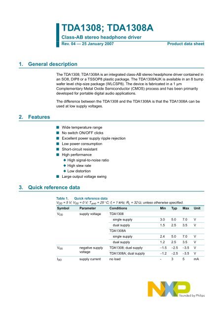
1. General description<br />
2. Features<br />
3. Quick reference data<br />
The <strong>TDA1308</strong>; <strong>TDA1308</strong>A is an integrated class-<strong>AB</strong> <strong>stereo</strong> <strong>headphone</strong> <strong>driver</strong> contained in<br />
an SO8, DIP8 or a TSSOP8 plastic package. The <strong>TDA1308</strong>AUK is available in an 8 bump<br />
wafer level chip-size package (WLCSP8). The device is fabricated in a 1 µm<br />
Complementary Metal Oxide Semiconductor (CMOS) process and has been primarily<br />
developed for portable digital audio applications.<br />
The difference between the <strong>TDA1308</strong> and the <strong>TDA1308</strong>A is that the <strong>TDA1308</strong>A can be<br />
used at low supply voltages.<br />
■ Wide temperature range<br />
■ No switch ON/OFF clicks<br />
■ Excellent power supply ripple rejection<br />
■ Low power consumption<br />
■ Short-circuit resistant<br />
■ High performance<br />
◆ High signal-to-noise ratio<br />
◆ High slew rate<br />
◆ Low distortion<br />
■ Large output voltage swing<br />
Table 1. Quick reference data<br />
V DD =5V; V SS =0V; T amb =25°C; f i = 1 kHz; R L =32Ω; unless otherwise specified.<br />
Symbol Parameter Conditions Min Typ Max Unit<br />
V DD supply voltage <strong>TDA1308</strong><br />
single supply 3.0 5.0 7.0 V<br />
dual supply 1.5 2.5 3.5 V<br />
<strong>TDA1308</strong>A<br />
single supply 2.4 5.0 7.0 V<br />
dual supply 1.2 2.5 3.5 V<br />
V SS negative supply <strong>TDA1308</strong>; dual supply −1.5 −2.5 −3.5 V<br />
voltage<br />
<strong>TDA1308</strong>A; dual supply −1.2 −2.5 −3.5 V<br />
I DD supply current no load - 3 5 mA
NXP Semiconductors<br />
<strong>TDA1308</strong>; <strong>TDA1308</strong>A<br />
<strong>Class</strong>-<strong>AB</strong> <strong>stereo</strong> <strong>headphone</strong> <strong>driver</strong><br />
P tot<br />
P o<br />
(THD + N)/S<br />
S/N<br />
α cs<br />
PSRR<br />
4. Ordering information<br />
Table 1. Quick reference data …continued<br />
V DD =5V; V SS =0V; T amb =25°C; f i = 1 kHz; R L =32Ω; unless otherwise specified.<br />
Symbol Parameter Conditions Min Typ Max Unit<br />
T amb<br />
total power<br />
dissipation<br />
maximum output<br />
power<br />
total harmonic<br />
distortion plus<br />
noise-to-signal<br />
ratio<br />
signal-to-noise<br />
ratio<br />
channel<br />
separation<br />
power supply<br />
ripple rejection<br />
ambient<br />
temperature<br />
[1] V DD =5V; V O(p-p) = 3.5 V (at 0 dB).<br />
[2] V DD = 2.4 V; V O(p-p) = 1.62 V (at −4.8 dBV); for <strong>TDA1308</strong>A only.<br />
[3] V DD = 2.4 V; V O(p-p) = 1.19 V (at −7.96 dBV); for <strong>TDA1308</strong>A only.<br />
no load - 15 25 mW<br />
(THD + N)/S < 0.1 %<br />
[1]<br />
- 40 80 mW<br />
[1]<br />
- 0.03 0.06 %<br />
[1]<br />
- −70 −65 dB<br />
R L =5kΩ<br />
[2]<br />
- −92 −89 dB<br />
R L =5kΩ<br />
[3]<br />
- −52 −40 dB<br />
R L =5kΩ - −101 - dB<br />
100 110 - dB<br />
- 70 - dB<br />
R L =5kΩ<br />
[1]<br />
- 105 - dB<br />
f i = 100 Hz;<br />
V ripple(p-p) = 100 mV<br />
- 90 - dB<br />
−40 - +85 °C<br />
Table 2.<br />
Type number<br />
Ordering information<br />
Package<br />
Name Description Version<br />
<strong>TDA1308</strong> DIP8 plastic dual in-line package; 8 leads (300 mil) SOT97-1<br />
<strong>TDA1308</strong>T SO8 plastic small outline package; 8 leads; body width SOT96-1<br />
3.9 mm<br />
<strong>TDA1308</strong>AT SO8 plastic small outline package; 8 leads; body width SOT96-1<br />
3.9 mm<br />
<strong>TDA1308</strong>AUK WLCSP8 wafer level chip-size package; 8 bumps;<br />
<strong>TDA1308</strong>AUK<br />
0.61 × 0.84 × 0.38 mm<br />
<strong>TDA1308</strong>TT TSSOP8 plastic thin shrink small outline package; 8 leads;<br />
body width 3 mm<br />
SOT505-1<br />
<strong>TDA1308</strong>_A_4<br />
© NXP B.V. 2007. All rights reserved.<br />
Product data sheet Rev. 04 — 25 January 2007 2 of 19
NXP Semiconductors<br />
<strong>TDA1308</strong>; <strong>TDA1308</strong>A<br />
<strong>Class</strong>-<strong>AB</strong> <strong>stereo</strong> <strong>headphone</strong> <strong>driver</strong><br />
5. Block diagram<br />
OUTA<br />
1<br />
<strong>TDA1308</strong>(A)<br />
8<br />
V DD<br />
INA(neg)<br />
INA(pos)<br />
2<br />
3<br />
7<br />
OUTB<br />
V SS<br />
4<br />
6<br />
5<br />
INB(neg)<br />
INB(pos)<br />
mka779<br />
Fig 1.<br />
Block diagram<br />
6. Pinning information<br />
6.1 Pinning<br />
bump A1<br />
index area<br />
<strong>TDA1308</strong>AUK<br />
1 2 3<br />
A<br />
B<br />
<strong>TDA1308</strong>(A)<br />
C<br />
OUTA<br />
1<br />
8<br />
V DD<br />
D<br />
INA(neg)<br />
2<br />
7<br />
OUTB<br />
INA(pos)<br />
3<br />
6<br />
INB(neg)<br />
E<br />
V SS<br />
4<br />
001aaf782<br />
5<br />
INB(pos)<br />
001aaf800<br />
Transparent top view<br />
Fig 2. Pin configuration <strong>TDA1308</strong>(A) Fig 3. Pin configuration <strong>TDA1308</strong>AUK<br />
6.2 Pin description<br />
Table 3. Pin description <strong>TDA1308</strong>(A)<br />
Symbol Pin Description<br />
OUTA 1 output A<br />
INA(neg) 2 inverting input A<br />
INA(pos) 3 non-inverting input A<br />
V SS 4 negative supply<br />
INB(pos) 5 non-inverting input B<br />
<strong>TDA1308</strong>_A_4<br />
© NXP B.V. 2007. All rights reserved.<br />
Product data sheet Rev. 04 — 25 January 2007 3 of 19
NXP Semiconductors<br />
<strong>TDA1308</strong>; <strong>TDA1308</strong>A<br />
<strong>Class</strong>-<strong>AB</strong> <strong>stereo</strong> <strong>headphone</strong> <strong>driver</strong><br />
Table 3. Pin description <strong>TDA1308</strong>(A) …continued<br />
Symbol Pin Description<br />
INB(neg) 6 inverting input B<br />
OUTB 7 output B<br />
V DD 8 positive supply<br />
7. Internal circuitry<br />
Table 4. Pin description <strong>TDA1308</strong>AUK<br />
Symbol Pin Description<br />
OUTA A1 output A<br />
V SS A3 negative supply<br />
INA(pos) B2 non-inverting input A<br />
OUTB C1 output B<br />
INA(neg) C3 inverting input A<br />
INB(neg) D2 inverting input B<br />
V DD E1 positive supply<br />
INB(pos) E3 non-inverting input B<br />
V DD<br />
I 1<br />
INA/B(pos)<br />
M1<br />
M2<br />
A1<br />
M3<br />
INA/B(neg)<br />
OUTA/B<br />
Cm<br />
D1<br />
D2<br />
D3<br />
D4<br />
M4<br />
M5<br />
A2<br />
M6<br />
V SS<br />
mka781<br />
Fig 4.<br />
Equivalent schematic diagram<br />
<strong>TDA1308</strong>_A_4<br />
© NXP B.V. 2007. All rights reserved.<br />
Product data sheet Rev. 04 — 25 January 2007 4 of 19
NXP Semiconductors<br />
<strong>TDA1308</strong>; <strong>TDA1308</strong>A<br />
<strong>Class</strong>-<strong>AB</strong> <strong>stereo</strong> <strong>headphone</strong> <strong>driver</strong><br />
8. Limiting values<br />
9. Thermal characteristics<br />
Table 5. Limiting values<br />
In accordance with the Absolute Maximum Rating System (IEC 60134).<br />
Symbol Parameter Conditions Min Max Unit<br />
V DD supply voltage 0 8.0 V<br />
t SC(O) output short-circuit duration T amb =25°C;<br />
20 - s<br />
P tot =1W<br />
T stg storage temperature −65 +150 °C<br />
T amb ambient temperature −40 +85 °C<br />
V esd electrostatic discharge HBM<br />
[1]<br />
−2 +2 kV<br />
voltage<br />
MM<br />
[2]<br />
−200 +200 V<br />
[1] Human body model (HBM): C = 100 pF; R = 1500 Ω; 3 pulses positive plus 3 pulses negative.<br />
[2] Machine model (MM): C = 200 pF; L = 0.5 mH; R = 0 Ω; 3 pulses positive plus 3 pulses negative.<br />
Table 6.<br />
Thermal characteristics<br />
Symbol Parameter Conditions Typ Unit<br />
R th(j-a) thermal resistance from junction<br />
to ambient<br />
DIP8 109 K/W<br />
SO8 210 K/W<br />
TSSOP8 220 K/W<br />
WLCSP8 1000 K/W<br />
<strong>TDA1308</strong>_A_4<br />
© NXP B.V. 2007. All rights reserved.<br />
Product data sheet Rev. 04 — 25 January 2007 5 of 19
NXP Semiconductors<br />
<strong>TDA1308</strong>; <strong>TDA1308</strong>A<br />
<strong>Class</strong>-<strong>AB</strong> <strong>stereo</strong> <strong>headphone</strong> <strong>driver</strong><br />
10. Characteristics<br />
Table 7. Characteristics<br />
V DD =5V; V SS =0V; T amb =25°C; f i = 1 kHz; R L =32Ω; unless otherwise specified.<br />
Symbol Parameter Conditions Min Typ Max Unit<br />
Supplies<br />
V DD supply voltage <strong>TDA1308</strong><br />
single supply 3.0 5.0 7.0 V<br />
dual supply 1.5 2.5 3.5 V<br />
<strong>TDA1308</strong>A<br />
single supply 2.4 5.0 7.0 V<br />
dual supply 1.2 2.5 3.5 V<br />
V SS negative supply voltage <strong>TDA1308</strong>; dual supply −1.5 −2.5 −3.5 V<br />
<strong>TDA1308</strong>A; dual supply −1.2 −2.5 −3.5 V<br />
I DD supply current no load - 3 5 mA<br />
P tot total power dissipation no load - 15 25 mW<br />
Static characteristics<br />
V I(os) input offset voltage - 10 - mV<br />
I bias input bias current - 10 - pA<br />
V CM common mode voltage 0 - 3.5 pA<br />
G V open-loop voltage gain R L =5kΩ - 70 - dB<br />
I O maximum output current - 60 - mA<br />
R O output resistance (THD + N)/S < 0.1 % - 0.25 - Ω<br />
V O output voltage swing<br />
[1]<br />
0.75 - 4.25 V<br />
R L =16Ω<br />
[1]<br />
1.5 - 3.5 V<br />
R L =5kΩ<br />
[1]<br />
0.1 - 4.9 V<br />
α cs channel separation - 70 - dB<br />
R L =5kΩ<br />
[1]<br />
- 105 - dB<br />
PSRR power supply ripple rejection f i = 100 Hz; V ripple(p-p) = 100 mV - 90 - dB<br />
C L load capacitance - - 200 pF<br />
Dynamic characteristics<br />
(THD + N)/S total harmonic distortion<br />
[2]<br />
- 0.03 0.06 %<br />
plus noise-to-signal ratio<br />
[2] - −70 −65 dB<br />
R L =5kΩ [3] - −92 −89 dB<br />
R L =5kΩ [3] - −52 −40 dB<br />
R L =5kΩ [3] - 0.25 1.0 %<br />
R L =5kΩ [2] - −101 - dB<br />
R L =5kΩ [2] - 0.0009 - %<br />
S/N signal-to-noise ratio 100 110 - dB<br />
f G unity gain frequency open-loop; R L =5kΩ - 5.5 - MHz<br />
P o maximum output power (THD + N)/S < 0.1 % - 40 80 mW<br />
<strong>TDA1308</strong>_A_4<br />
© NXP B.V. 2007. All rights reserved.<br />
Product data sheet Rev. 04 — 25 January 2007 6 of 19
NXP Semiconductors<br />
<strong>TDA1308</strong>; <strong>TDA1308</strong>A<br />
<strong>Class</strong>-<strong>AB</strong> <strong>stereo</strong> <strong>headphone</strong> <strong>driver</strong><br />
Table 7. Characteristics …continued<br />
V DD =5V; V SS =0V; T amb =25°C; f i = 1 kHz; R L =32Ω; unless otherwise specified.<br />
Symbol Parameter Conditions Min Typ Max Unit<br />
C i input capacitance - 3 - pF<br />
SR slew rate unity gain inverting - 5 - V/µs<br />
B bandwidth unity gain inverting - 20 - kHz<br />
[1] Values are proportional to V DD ; (THD + N)/S < 0.1 %.<br />
[2] V DD =5V; V O(p-p) = 3.5 V (at 0 dB).<br />
[3] V DD = 2.4 V; V O(p-p) = 1.19 V (at −7.96 dBV); for <strong>TDA1308</strong>A only.<br />
11. Application information<br />
V DD<br />
C2<br />
10 µF<br />
C1<br />
100 nF<br />
R1<br />
22 kΩ<br />
C5<br />
1 nF<br />
R3<br />
3.9 kΩ<br />
C7<br />
100 µF<br />
R5<br />
10 kΩ<br />
BCK<br />
1<br />
5<br />
8<br />
2<br />
3<br />
1<br />
8<br />
WS<br />
DATA<br />
2 TDA1545A 7<br />
3 6<br />
4<br />
R2<br />
33 kΩ<br />
V ref<br />
C3<br />
1 µF<br />
5<br />
6<br />
R4<br />
<strong>TDA1308</strong>(A)<br />
7 4<br />
C6<br />
100 µF<br />
3.9 kΩ<br />
C8<br />
C4<br />
1 nF<br />
100 µF<br />
R6<br />
10 kΩ<br />
mka783<br />
Fig 5.<br />
Example of application with TDA1545A (<strong>stereo</strong> continuous calibration DAC)<br />
<strong>TDA1308</strong>_A_4<br />
© NXP B.V. 2007. All rights reserved.<br />
Product data sheet Rev. 04 — 25 January 2007 7 of 19
NXP Semiconductors<br />
<strong>TDA1308</strong>; <strong>TDA1308</strong>A<br />
<strong>Class</strong>-<strong>AB</strong> <strong>stereo</strong> <strong>headphone</strong> <strong>driver</strong><br />
12. Test information<br />
V DD<br />
3.9 kΩ<br />
100 µF<br />
V OUTA<br />
RL<br />
V INA<br />
3.9 kΩ<br />
2<br />
3<br />
1<br />
8<br />
V ref<br />
(typ. 2.5 V)<br />
V INB<br />
3.9 kΩ<br />
5<br />
6<br />
<strong>TDA1308</strong>(A)<br />
C6<br />
100 µF<br />
7 4<br />
3.9 kΩ<br />
100 µF<br />
V OUTB<br />
RL<br />
mka782<br />
Fig 6.<br />
Measurement circuit for inverting application<br />
mka784<br />
−70<br />
mka785<br />
80<br />
G v<br />
(dB)<br />
G v<br />
(dB)<br />
−90<br />
40<br />
R L = 32 Ω<br />
no load<br />
R L = 16 Ω<br />
−110<br />
32 Ω<br />
0<br />
5 kΩ<br />
10 −2 10 −3 10 −4 10 −5 10 −6 10 −7 10 −8<br />
f i (Hz)<br />
−130<br />
10 −1 10 −2 10 −3 10 −4 10<br />
f −5<br />
i (Hz)<br />
Fig 7. Open-loop gain as a function of input frequency Fig 8. Crosstalk as a function of input frequency<br />
<strong>TDA1308</strong>_A_4<br />
© NXP B.V. 2007. All rights reserved.<br />
Product data sheet Rev. 04 — 25 January 2007 8 of 19
NXP Semiconductors<br />
<strong>TDA1308</strong>; <strong>TDA1308</strong>A<br />
<strong>Class</strong>-<strong>AB</strong> <strong>stereo</strong> <strong>headphone</strong> <strong>driver</strong><br />
100<br />
mka786<br />
−50<br />
mka787<br />
P o<br />
(mW)<br />
60<br />
40<br />
R L = 16 Ω<br />
32 Ω<br />
8 Ω<br />
(THD+N)/S<br />
(dB)<br />
−70<br />
R L = 16 Ω; P o = 50 mW<br />
R L = 32 Ω; P o = 50 mW<br />
20<br />
−90<br />
R L = 5 kΩ; V O(p−p) = 3.5 V<br />
10<br />
3<br />
4<br />
5<br />
V DD (V)<br />
−110<br />
10 −1 10 −2 10 −3 10 −4 f i (Hz)<br />
10 −5<br />
Fig 9. Output power as a function of supply voltage Fig 10. Total harmonic distortion plus noise-to-signal<br />
ratio as a function of input frequency<br />
−40<br />
mka788<br />
(THD+N)/S<br />
(dB)<br />
−60<br />
R L = 8 Ω<br />
16 Ω<br />
32 Ω<br />
−80<br />
5 kΩ<br />
f i = 1 kHz<br />
−100<br />
10 −2 10 −1 1<br />
V O(p−p) (V)<br />
10<br />
Fig 11. Total harmonic distortion plus noise-to-signal ratio as a function of output voltage<br />
level<br />
12.1 Quality information<br />
The General Quality Specification for Integrated Circuits, SNW-FQ-611 is applicable.<br />
<strong>TDA1308</strong>_A_4<br />
© NXP B.V. 2007. All rights reserved.<br />
Product data sheet Rev. 04 — 25 January 2007 9 of 19
NXP Semiconductors<br />
<strong>TDA1308</strong>; <strong>TDA1308</strong>A<br />
<strong>Class</strong>-<strong>AB</strong> <strong>stereo</strong> <strong>headphone</strong> <strong>driver</strong><br />
13. Package outline<br />
DIP8: plastic dual in-line package; 8 leads (300 mil)<br />
SOT97-1<br />
D<br />
M E<br />
seating plane<br />
A 2<br />
A<br />
L<br />
A 1<br />
w M<br />
Z<br />
e<br />
b 1<br />
c<br />
(e ) 1<br />
8<br />
b<br />
5<br />
b 2<br />
M H<br />
pin 1 index<br />
E<br />
1<br />
4<br />
0 5 10 mm<br />
scale<br />
DIMENSIONS (inch dimensions are derived from the original mm dimensions)<br />
A A<br />
UNIT<br />
1 A 2 (1) (1)<br />
(1)<br />
max.<br />
b 1 b 2 c D E e L<br />
M Z<br />
min. max.<br />
b<br />
e 1<br />
M E H w<br />
max.<br />
1.73 0.53 1.07 0.36 9.8 6.48<br />
3.60 8.25 10.0<br />
mm 4.2 0.51 3.2<br />
2.54 7.62<br />
0.254 1.15<br />
1.14 0.38 0.89 0.23 9.2 6.20<br />
3.05 7.80 8.3<br />
inches<br />
0.17 0.02 0.13<br />
0.068<br />
0.045<br />
0.021<br />
0.015<br />
0.042<br />
0.035<br />
0.014<br />
0.009<br />
0.39<br />
0.36<br />
0.26<br />
0.24<br />
Note<br />
1. Plastic or metal protrusions of 0.25 mm (0.01 inch) maximum per side are not included.<br />
0.1 0.3<br />
0.14<br />
0.12<br />
0.32<br />
0.31<br />
0.39<br />
0.33<br />
0.01<br />
0.045<br />
OUTLINE<br />
VERSION<br />
REFERENCES<br />
IEC JEDEC JEITA<br />
EUROPEAN<br />
PROJECTION<br />
ISSUE DATE<br />
SOT97-1<br />
050G01 MO-001 SC-504-8<br />
99-12-27<br />
03-02-13<br />
Fig 12. Package outline SOT97-1 (DIP8)<br />
<strong>TDA1308</strong>_A_4<br />
© NXP B.V. 2007. All rights reserved.<br />
Product data sheet Rev. 04 — 25 January 2007 10 of 19
NXP Semiconductors<br />
<strong>TDA1308</strong>; <strong>TDA1308</strong>A<br />
<strong>Class</strong>-<strong>AB</strong> <strong>stereo</strong> <strong>headphone</strong> <strong>driver</strong><br />
SO8: plastic small outline package; 8 leads; body width 3.9 mm<br />
SOT96-1<br />
D<br />
E<br />
A<br />
X<br />
c<br />
y<br />
H E<br />
v M<br />
A<br />
Z<br />
8<br />
5<br />
pin 1 index<br />
A 2<br />
A 1<br />
L p<br />
Q<br />
(A ) 3<br />
θ<br />
A<br />
1<br />
4<br />
L<br />
e<br />
b p<br />
w M<br />
detail X<br />
0 2.5 5 mm<br />
scale<br />
DIMENSIONS (inch dimensions are derived from the original mm dimensions)<br />
UNIT<br />
mm<br />
inches<br />
A<br />
max.<br />
1.75<br />
A 1 A 2 A 3 b p c D (1) E (2) e H (1)<br />
E L L p Q v w y Z<br />
0.25<br />
0.10<br />
0.069 0.010<br />
0.004<br />
1.45<br />
1.25<br />
0.057<br />
0.049<br />
0.25<br />
0.01<br />
0.49<br />
0.36<br />
0.019<br />
0.014<br />
0.25<br />
0.19<br />
0.0100<br />
0.0075<br />
Notes<br />
1. Plastic or metal protrusions of 0.15 mm (0.006 inch) maximum per side are not included.<br />
2. Plastic or metal protrusions of 0.25 mm (0.01 inch) maximum per side are not included.<br />
5.0<br />
4.8<br />
0.20<br />
0.19<br />
4.0<br />
3.8<br />
0.16<br />
0.15<br />
1.27<br />
0.05<br />
6.2<br />
5.8<br />
0.244<br />
0.228<br />
1.05<br />
1.0<br />
0.4<br />
0.7<br />
0.6<br />
0.25<br />
0.25 0.1<br />
0.039 0.028<br />
0.041 0.01 0.01 0.004<br />
0.016 0.024<br />
θ<br />
0.7<br />
0.3 o<br />
8<br />
o<br />
0.028 0<br />
0.012<br />
OUTLINE<br />
VERSION<br />
REFERENCES<br />
IEC JEDEC JEITA<br />
EUROPEAN<br />
PROJECTION<br />
ISSUE DATE<br />
SOT96-1<br />
076E03 MS-012<br />
99-12-27<br />
03-02-18<br />
Fig 13. Package outline SOT96-1 (SO8)<br />
<strong>TDA1308</strong>_A_4<br />
© NXP B.V. 2007. All rights reserved.<br />
Product data sheet Rev. 04 — 25 January 2007 11 of 19
NXP Semiconductors<br />
<strong>TDA1308</strong>; <strong>TDA1308</strong>A<br />
<strong>Class</strong>-<strong>AB</strong> <strong>stereo</strong> <strong>headphone</strong> <strong>driver</strong><br />
TSSOP8: plastic thin shrink small outline package; 8 leads; body width 3 mm<br />
SOT505-1<br />
y<br />
D<br />
c<br />
H E<br />
E<br />
A<br />
X<br />
v M<br />
A<br />
Z<br />
8 5<br />
pin 1 index<br />
A 2 A1<br />
L p<br />
(A 3 )<br />
A<br />
θ<br />
1 4<br />
e<br />
b p<br />
w M<br />
L<br />
detail X<br />
0<br />
2.5 5 mm<br />
scale<br />
DIMENSIONS (mm are the original dimensions)<br />
A<br />
UNIT A<br />
max. 1<br />
mm<br />
1.1<br />
0.15<br />
0.05<br />
A 2 A 3 b p c D (1) E (2) e H E L L p v w y Z (1) θ<br />
0.95<br />
0.80<br />
0.25<br />
0.45<br />
0.25<br />
0.28<br />
0.15<br />
3.1<br />
2.9<br />
3.1<br />
2.9<br />
0.65<br />
5.1<br />
4.7<br />
0.94<br />
0.7<br />
0.4<br />
0.1<br />
0.1 0.1<br />
0.70<br />
0.35<br />
6°<br />
0°<br />
Notes<br />
1. Plastic or metal protrusions of 0.15 mm maximum per side are not included.<br />
2. Plastic or metal protrusions of 0.25 mm maximum per side are not included.<br />
OUTLINE<br />
VERSION<br />
REFERENCES<br />
IEC JEDEC JEITA<br />
EUROPEAN<br />
PROJECTION<br />
ISSUE DATE<br />
SOT505-1<br />
99-04-09<br />
03-02-18<br />
Fig 14. Package outline SOT505-1 (TSSOP8)<br />
<strong>TDA1308</strong>_A_4<br />
© NXP B.V. 2007. All rights reserved.<br />
Product data sheet Rev. 04 — 25 January 2007 12 of 19
NXP Semiconductors<br />
<strong>TDA1308</strong>; <strong>TDA1308</strong>A<br />
<strong>Class</strong>-<strong>AB</strong> <strong>stereo</strong> <strong>headphone</strong> <strong>driver</strong><br />
WLCSP8: wafer level chip-size package; 8 bumps; 0.61 x 0.84 x 0.38 mm<br />
<strong>TDA1308</strong>AUK<br />
D<br />
B<br />
A<br />
bump A1<br />
index area<br />
A 2<br />
A 1<br />
detail X<br />
E<br />
A<br />
e 1<br />
1/4 e 2<br />
1/2 e 2<br />
1/2 e 1<br />
∅ v M C A<br />
b<br />
∅ w M C<br />
B<br />
C<br />
y<br />
E<br />
D<br />
C<br />
e 2<br />
B<br />
A<br />
1 2<br />
3<br />
DIMENSIONS (mm are the original dimensions)<br />
UNIT<br />
A<br />
max<br />
mm 0.49<br />
A 1<br />
0.10<br />
0.07<br />
A 2<br />
0.39<br />
0.37<br />
b<br />
0.123<br />
0.091<br />
D E e 1 e 2 v<br />
0.65<br />
0.57<br />
0.88<br />
0.80<br />
0 0.25 0.5 mm<br />
scale<br />
0.396 0.588 0.15 0.05 0.08<br />
w<br />
y<br />
X<br />
OUTLINE<br />
VERSION<br />
<strong>TDA1308</strong>AUK<br />
REFERENCES<br />
IEC JEDEC JEITA<br />
EUROPEAN<br />
PROJECTION<br />
ISSUE DATE<br />
06-11-20<br />
06-12-15<br />
Fig 15. Package outline <strong>TDA1308</strong>AUK (WLCSP8)<br />
<strong>TDA1308</strong>_A_4<br />
© NXP B.V. 2007. All rights reserved.<br />
Product data sheet Rev. 04 — 25 January 2007 13 of 19
NXP Semiconductors<br />
<strong>TDA1308</strong>; <strong>TDA1308</strong>A<br />
<strong>Class</strong>-<strong>AB</strong> <strong>stereo</strong> <strong>headphone</strong> <strong>driver</strong><br />
14. Soldering<br />
This text provides a very brief insight into a complex technology. A more in-depth account<br />
of soldering ICs can be found in Application Note AN10365 “Surface mount reflow<br />
soldering description”.<br />
14.1 Introduction to soldering<br />
Soldering is one of the most common methods through which packages are attached to<br />
Printed Circuit Boards (PCBs), to form electrical circuits. The soldered joint provides both<br />
the mechanical and the electrical connection. There is no single soldering method that is<br />
ideal for all IC packages. Wave soldering is often preferred when through-hole and<br />
Surface Mount Devices (SMDs) are mixed on one printed wiring board; however, it is not<br />
suitable for fine pitch SMDs. Reflow soldering is ideal for the small pitches and high<br />
densities that come with increased miniaturization.<br />
14.2 Wave and reflow soldering<br />
Wave soldering is a joining technology in which the joints are made by solder coming from<br />
a standing wave of liquid solder. The wave soldering process is suitable for the following:<br />
• Through-hole components<br />
• Leaded or leadless SMDs, which are glued to the surface of the printed circuit board<br />
Not all SMDs can be wave soldered. Packages with solder balls, and some leadless<br />
packages which have solder lands underneath the body, cannot be wave soldered. Also,<br />
leaded SMDs with leads having a pitch smaller than ~0.6 mm cannot be wave soldered,<br />
due to an increased probability of bridging.<br />
The reflow soldering process involves applying solder paste to a board, followed by<br />
component placement and exposure to a temperature profile. Leaded packages,<br />
packages with solder balls, and leadless packages are all reflow solderable.<br />
Key characteristics in both wave and reflow soldering are:<br />
• Board specifications, including the board finish, solder masks and vias<br />
• Package footprints, including solder thieves and orientation<br />
• The moisture sensitivity level of the packages<br />
• Package placement<br />
• Inspection and repair<br />
• Lead-free soldering versus PbSn soldering<br />
14.3 Wave soldering<br />
Key characteristics in wave soldering are:<br />
• Process issues, such as application of adhesive and flux, clinching of leads, board<br />
transport, the solder wave parameters, and the time during which components are<br />
exposed to the wave<br />
• Solder bath specifications, including temperature and impurities<br />
<strong>TDA1308</strong>_A_4<br />
© NXP B.V. 2007. All rights reserved.<br />
Product data sheet Rev. 04 — 25 January 2007 14 of 19
NXP Semiconductors<br />
<strong>TDA1308</strong>; <strong>TDA1308</strong>A<br />
<strong>Class</strong>-<strong>AB</strong> <strong>stereo</strong> <strong>headphone</strong> <strong>driver</strong><br />
14.4 Reflow soldering<br />
Key characteristics in reflow soldering are:<br />
• Lead-free versus SnPb soldering; note that a lead-free reflow process usually leads to<br />
higher minimum peak temperatures (see Figure 16) than a PbSn process, thus<br />
reducing the process window<br />
• Solder paste printing issues including smearing, release, and adjusting the process<br />
window for a mix of large and small components on one board<br />
• Reflow temperature profile; this profile includes preheat, reflow (in which the board is<br />
heated to the peak temperature) and cooling down. It is imperative that the peak<br />
temperature is high enough for the solder to make reliable solder joints (a solder paste<br />
characteristic). In addition, the peak temperature must be low enough that the<br />
packages and/or boards are not damaged. The peak temperature of the package<br />
depends on package thickness and volume and is classified in accordance with<br />
Table 8 and 9<br />
Table 8.<br />
SnPb eutectic process (from J-STD-020C)<br />
Package thickness (mm)<br />
Package reflow temperature (°C)<br />
Volume (mm 3 )<br />
< 350 ≥ 350<br />
< 2.5 235 220<br />
≥ 2.5 220 220<br />
Table 9. Lead-free process (from J-STD-020C)<br />
Package thickness (mm) Package reflow temperature (°C)<br />
Volume (mm 3 )<br />
< 350 350 to 2000 > 2000<br />
< 1.6 260 260 260<br />
1.6 to 2.5 260 250 245<br />
> 2.5 250 245 245<br />
Moisture sensitivity precautions, as indicated on the packing, must be respected at all<br />
times.<br />
Studies have shown that small packages reach higher temperatures during reflow<br />
soldering, see Figure 16.<br />
<strong>TDA1308</strong>_A_4<br />
© NXP B.V. 2007. All rights reserved.<br />
Product data sheet Rev. 04 — 25 January 2007 15 of 19
NXP Semiconductors<br />
<strong>TDA1308</strong>; <strong>TDA1308</strong>A<br />
<strong>Class</strong>-<strong>AB</strong> <strong>stereo</strong> <strong>headphone</strong> <strong>driver</strong><br />
temperature<br />
maximum peak temperature<br />
= MSL limit, damage level<br />
minimum peak temperature<br />
= minimum soldering temperature<br />
peak<br />
temperature<br />
time<br />
001aac844<br />
MSL: Moisture Sensitivity Level<br />
Fig 16. Temperature profiles for large and small components<br />
For further information on temperature profiles, refer to Application Note AN10365<br />
“Surface mount reflow soldering description”.<br />
<strong>TDA1308</strong>_A_4<br />
© NXP B.V. 2007. All rights reserved.<br />
Product data sheet Rev. 04 — 25 January 2007 16 of 19
NXP Semiconductors<br />
<strong>TDA1308</strong>; <strong>TDA1308</strong>A<br />
<strong>Class</strong>-<strong>AB</strong> <strong>stereo</strong> <strong>headphone</strong> <strong>driver</strong><br />
15. Revision history<br />
Table 10.<br />
Revision history<br />
Document ID Release date Data sheet status Change notice Supersedes<br />
<strong>TDA1308</strong>_A_4 20070125 Product data sheet - <strong>TDA1308</strong>_A_3<br />
Modifications:<br />
• The format of this data sheet has been redesigned to comply with the new identity<br />
guidelines of NXP Semiconductors<br />
• Legal texts have been adapted to the new company name where appropriate<br />
• Type number <strong>TDA1308</strong>AUK has been added<br />
<strong>TDA1308</strong>_A_3 20020719 Product specification - <strong>TDA1308</strong>_A_2<br />
<strong>TDA1308</strong>_A_2 20020227 Product specification - <strong>TDA1308</strong>_1<br />
<strong>TDA1308</strong>_1 19940905 Product specification - -<br />
<strong>TDA1308</strong>_A_4<br />
© NXP B.V. 2007. All rights reserved.<br />
Product data sheet Rev. 04 — 25 January 2007 17 of 19
NXP Semiconductors<br />
<strong>TDA1308</strong>; <strong>TDA1308</strong>A<br />
<strong>Class</strong>-<strong>AB</strong> <strong>stereo</strong> <strong>headphone</strong> <strong>driver</strong><br />
16. Legal information<br />
16.1 Data sheet status<br />
Document status [1][2] Product status [3] Definition<br />
Objective [short] data sheet Development This document contains data from the objective specification for product development.<br />
Preliminary [short] data sheet Qualification This document contains data from the preliminary specification.<br />
Product [short] data sheet Production This document contains the product specification.<br />
[1] Please consult the most recently issued document before initiating or completing a design.<br />
[2] The term ‘short data sheet’ is explained in section “Definitions”.<br />
[3] The product status of device(s) described in this document may have changed since this document was published and may differ in case of multiple devices. The latest product status<br />
information is available on the Internet at URL http://www.nxp.com.<br />
16.2 Definitions<br />
Draft — The document is a draft version only. The content is still under<br />
internal review and subject to formal approval, which may result in<br />
modifications or additions. NXP Semiconductors does not give any<br />
representations or warranties as to the accuracy or completeness of<br />
information included herein and shall have no liability for the consequences of<br />
use of such information.<br />
Short data sheet — A short data sheet is an extract from a full data sheet<br />
with the same product type number(s) and title. A short data sheet is intended<br />
for quick reference only and should not be relied upon to contain detailed and<br />
full information. For detailed and full information see the relevant full data<br />
sheet, which is available on request via the local NXP Semiconductors sales<br />
office. In case of any inconsistency or conflict with the short data sheet, the<br />
full data sheet shall prevail.<br />
16.3 Disclaimers<br />
General — Information in this document is believed to be accurate and<br />
reliable. However, NXP Semiconductors does not give any representations or<br />
warranties, expressed or implied, as to the accuracy or completeness of such<br />
information and shall have no liability for the consequences of use of such<br />
information.<br />
Right to make changes — NXP Semiconductors reserves the right to make<br />
changes to information published in this document, including without<br />
limitation specifications and product descriptions, at any time and without<br />
notice. This document supersedes and replaces all information supplied prior<br />
to the publication hereof.<br />
Suitability for use — NXP Semiconductors products are not designed,<br />
authorized or warranted to be suitable for use in medical, military, aircraft,<br />
space or life support equipment, nor in applications where failure or<br />
malfunction of a NXP Semiconductors product can reasonably be expected to<br />
result in personal injury, death or severe property or environmental damage.<br />
NXP Semiconductors accepts no liability for inclusion and/or use of NXP<br />
Semiconductors products in such equipment or applications and therefore<br />
such inclusion and/or use is at the customer’s own risk.<br />
Applications — Applications that are described herein for any of these<br />
products are for illustrative purposes only. NXP Semiconductors makes no<br />
representation or warranty that such applications will be suitable for the<br />
specified use without further testing or modification.<br />
Limiting values — Stress above one or more limiting values (as defined in<br />
the Absolute Maximum Ratings System of IEC 60134) may cause permanent<br />
damage to the device. Limiting values are stress ratings only and operation of<br />
the device at these or any other conditions above those given in the<br />
Characteristics sections of this document is not implied. Exposure to limiting<br />
values for extended periods may affect device reliability.<br />
Terms and conditions of sale — NXP Semiconductors products are sold<br />
subject to the general terms and conditions of commercial sale, as published<br />
at http://www.nxp.com/profile/terms, including those pertaining to warranty,<br />
intellectual property rights infringement and limitation of liability, unless<br />
explicitly otherwise agreed to in writing by NXP Semiconductors. In case of<br />
any inconsistency or conflict between information in this document and such<br />
terms and conditions, the latter will prevail.<br />
No offer to sell or license — Nothing in this document may be interpreted<br />
or construed as an offer to sell products that is open for acceptance or the<br />
grant, conveyance or implication of any license under any copyrights, patents<br />
or other industrial or intellectual property rights.<br />
16.4 Trademarks<br />
Notice: All referenced brands, product names, service names and trademarks<br />
are the property of their respective owners.<br />
17. Contact information<br />
For additional information, please visit: http://www.nxp.com<br />
For sales office addresses, send an email to: salesaddresses@nxp.com<br />
<strong>TDA1308</strong>_A_4<br />
© NXP B.V. 2007. All rights reserved.<br />
Product data sheet Rev. 04 — 25 January 2007 18 of 19
NXP Semiconductors<br />
<strong>TDA1308</strong>; <strong>TDA1308</strong>A<br />
<strong>Class</strong>-<strong>AB</strong> <strong>stereo</strong> <strong>headphone</strong> <strong>driver</strong><br />
18. Contents<br />
1 General description . . . . . . . . . . . . . . . . . . . . . . 1<br />
2 Features . . . . . . . . . . . . . . . . . . . . . . . . . . . . . . . 1<br />
3 Quick reference data . . . . . . . . . . . . . . . . . . . . . 1<br />
4 Ordering information . . . . . . . . . . . . . . . . . . . . . 2<br />
5 Block diagram . . . . . . . . . . . . . . . . . . . . . . . . . . 3<br />
6 Pinning information . . . . . . . . . . . . . . . . . . . . . . 3<br />
6.1 Pinning . . . . . . . . . . . . . . . . . . . . . . . . . . . . . . . 3<br />
6.2 Pin description . . . . . . . . . . . . . . . . . . . . . . . . . 3<br />
7 Internal circuitry. . . . . . . . . . . . . . . . . . . . . . . . . 4<br />
8 Limiting values. . . . . . . . . . . . . . . . . . . . . . . . . . 5<br />
9 Thermal characteristics. . . . . . . . . . . . . . . . . . . 5<br />
10 Characteristics. . . . . . . . . . . . . . . . . . . . . . . . . . 6<br />
11 Application information. . . . . . . . . . . . . . . . . . . 7<br />
12 Test information . . . . . . . . . . . . . . . . . . . . . . . . . 8<br />
12.1 Quality information . . . . . . . . . . . . . . . . . . . . . . 9<br />
13 Package outline . . . . . . . . . . . . . . . . . . . . . . . . 10<br />
14 Soldering . . . . . . . . . . . . . . . . . . . . . . . . . . . . . 14<br />
14.1 Introduction to soldering . . . . . . . . . . . . . . . . . 14<br />
14.2 Wave and reflow soldering . . . . . . . . . . . . . . . 14<br />
14.3 Wave soldering . . . . . . . . . . . . . . . . . . . . . . . . 14<br />
14.4 Reflow soldering . . . . . . . . . . . . . . . . . . . . . . . 15<br />
15 Revision history . . . . . . . . . . . . . . . . . . . . . . . . 17<br />
16 Legal information. . . . . . . . . . . . . . . . . . . . . . . 18<br />
16.1 Data sheet status . . . . . . . . . . . . . . . . . . . . . . 18<br />
16.2 Definitions. . . . . . . . . . . . . . . . . . . . . . . . . . . . 18<br />
16.3 Disclaimers . . . . . . . . . . . . . . . . . . . . . . . . . . . 18<br />
16.4 Trademarks . . . . . . . . . . . . . . . . . . . . . . . . . . . 18<br />
17 Contact information. . . . . . . . . . . . . . . . . . . . . 18<br />
18 Contents . . . . . . . . . . . . . . . . . . . . . . . . . . . . . . 19<br />
Please be aware that important notices concerning this document and the product(s)<br />
described herein, have been included in section ‘Legal information’.<br />
© NXP B.V. 2007. All rights reserved.<br />
For more information, please visit: http://www.nxp.com<br />
For sales office addresses, please send an email to: salesaddresses@nxp.com<br />
Date of release: 25 January 2007<br />
Document identifier: <strong>TDA1308</strong>_A_4


