xmega a3u - Elfa
xmega a3u - Elfa
xmega a3u - Elfa
Create successful ePaper yourself
Turn your PDF publications into a flip-book with our unique Google optimized e-Paper software.
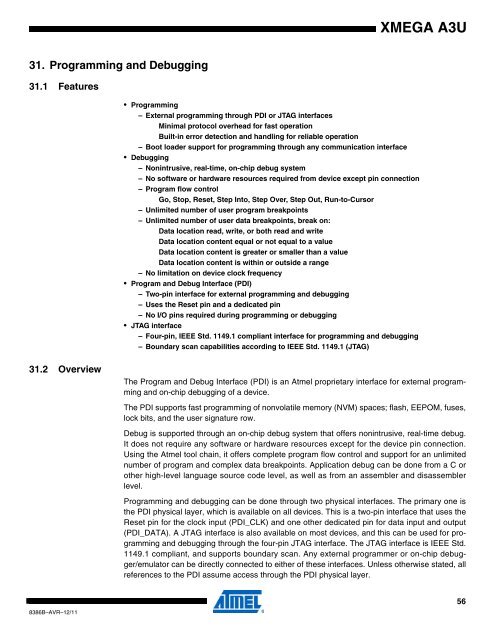
XMEGA A3U<br />
31. Programming and Debugging<br />
31.1 Features<br />
• Programming<br />
– External programming through PDI or JTAG interfaces<br />
Minimal protocol overhead for fast operation<br />
Built-in error detection and handling for reliable operation<br />
– Boot loader support for programming through any communication interface<br />
• Debugging<br />
– Nonintrusive, real-time, on-chip debug system<br />
– No software or hardware resources required from device except pin connection<br />
– Program flow control<br />
Go, Stop, Reset, Step Into, Step Over, Step Out, Run-to-Cursor<br />
– Unlimited number of user program breakpoints<br />
– Unlimited number of user data breakpoints, break on:<br />
Data location read, write, or both read and write<br />
Data location content equal or not equal to a value<br />
Data location content is greater or smaller than a value<br />
Data location content is within or outside a range<br />
– No limitation on device clock frequency<br />
• Program and Debug Interface (PDI)<br />
– Two-pin interface for external programming and debugging<br />
– Uses the Reset pin and a dedicated pin<br />
– No I/O pins required during programming or debugging<br />
• JTAG interface<br />
– Four-pin, IEEE Std. 1149.1 compliant interface for programming and debugging<br />
– Boundary scan capabilities according to IEEE Std. 1149.1 (JTAG)<br />
31.2 Overview<br />
The Program and Debug Interface (PDI) is an Atmel proprietary interface for external programming<br />
and on-chip debugging of a device.<br />
The PDI supports fast programming of nonvolatile memory (NVM) spaces; flash, EEPOM, fuses,<br />
lock bits, and the user signature row.<br />
Debug is supported through an on-chip debug system that offers nonintrusive, real-time debug.<br />
It does not require any software or hardware resources except for the device pin connection.<br />
Using the Atmel tool chain, it offers complete program flow control and support for an unlimited<br />
number of program and complex data breakpoints. Application debug can be done from a C or<br />
other high-level language source code level, as well as from an assembler and disassembler<br />
level.<br />
Programming and debugging can be done through two physical interfaces. The primary one is<br />
the PDI physical layer, which is available on all devices. This is a two-pin interface that uses the<br />
Reset pin for the clock input (PDI_CLK) and one other dedicated pin for data input and output<br />
(PDI_DATA). A JTAG interface is also available on most devices, and this can be used for programming<br />
and debugging through the four-pin JTAG interface. The JTAG interface is IEEE Std.<br />
1149.1 compliant, and supports boundary scan. Any external programmer or on-chip debugger/emulator<br />
can be directly connected to either of these interfaces. Unless otherwise stated, all<br />
references to the PDI assume access through the PDI physical layer.<br />
8386B–AVR–12/11<br />
56


