

Notes SM72295 Photovoltaic Full Bridge Driver
Notes SM72295 Photovoltaic Full Bridge Driver
Notes SM72295 Photovoltaic Full Bridge Driver

Create successful ePaper yourself
Turn your PDF publications into a flip-book with our unique Google optimized e-Paper software.
<strong>Photovoltaic</strong> <strong>Full</strong> <strong>Bridge</strong> <strong>Driver</strong><br />
General Description<br />
The <strong>SM72295</strong> is designed to drive 4 discrete N type<br />
MOSFET’s in a full bridge configuration. The drivers provide<br />
3A of peak current for fast efficient switching and integrated<br />
high speed bootstrap diodes. Current sensing is provided by<br />
2 transconductance amplifiers with externally programmable<br />
gain and filtering to remove ripple current to provide average<br />
current information to the control circuit. The current sense<br />
amplifiers have buffered outputs available to provide a low<br />
impedance interface to an A/D converter if needed. An externally<br />
programmable input over voltage comparator is also<br />
included to shutdown all outputs. Under voltage lockout with<br />
a PGOOD indicator prevents the drivers from operating if<br />
VCC is too low.<br />
<strong>SM72295</strong><br />
Features<br />
February 25, 2011<br />
■ Renewable Energy Grade<br />
■ Dual Half <strong>Bridge</strong> MOSFET <strong>Driver</strong>s<br />
■ Integrated 100V bootstrap diodes<br />
■ Independent High and Low driver logic inputs<br />
■ Bootstrap supply voltage range up to 115V DC<br />
■ Two current sense amplifiers with externally<br />
programmable gain and buffered outputs<br />
■ Programmable over voltage protection<br />
■ Supply rail under-voltage lockouts with power good<br />
indicator<br />
Package<br />
■ SOIC-28<br />
<strong>SM72295</strong> <strong>Photovoltaic</strong> <strong>Full</strong> <strong>Bridge</strong> <strong>Driver</strong><br />
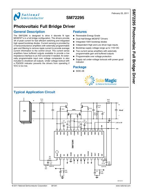
Typical Application Circuit<br />
30134101<br />
© 2011 National Semiconductor Corporation 301341 www.national.com
<strong>SM72295</strong><br />
Connection Diagram<br />
Top View<br />
SOIC-28<br />
30134116<br />
Ordering Information<br />
Order Number Description NSC Package Drawing Supplied As<br />
<strong>SM72295</strong>X 28L SOIC WIDE M28B 1000 Units in Tape and Reel<br />
<strong>SM72295</strong>E 28L SOIC WIDE M28B 250 Units in Tape and Reel<br />
www.national.com 2
Pin Descriptions<br />
Pin Name Description Application Information<br />
5 AGND Analog ground Ground return for the analog circuitry. Tie to the ground plane under the IC<br />
23 PGND Power ground return Ground return for the LO drivers. Tie to the ground plane under the IC<br />
21,25 VCCA,<br />
VCCB<br />
26,20 HBA,<br />
HBB<br />
27, 19 HOA,<br />
HOB<br />
28, 18 HSA,<br />
HSB<br />
Positive gate drive supply<br />
High side gate driver bootstrap<br />
rail.<br />
High side gate driver output<br />
High side MOSFET source<br />
connection<br />
Locally decouple to PGND using low ESR/ESL capacitor located as close to IC<br />
as possible.<br />
Connect the positive terminal of the bootstrap capacitor to HB and the negative<br />
terminal to HS. The bootstrap capacitor should be placed as close to IC as<br />
possible.<br />
Connect to gate of high side MOSFET with a short low inductance path.<br />
Connect to bootstrap capacitor negative terminal and the source of the high side<br />
MOSFET.<br />
7, 8 HIA, HIB High side driver control input The inputs have TTL type thresholds. Unused inputs should be tied to ground<br />
and not left open.<br />
6, 9 LIA, LIB Low side driver control input The inputs have TTL type thresholds. Unused inputs should be tied to ground<br />
and not left open.<br />
24, 22 LOA,<br />
LOB<br />
Low side gate driver output<br />
Connect to the gate of the low side MOSFET with a short low inductance path.<br />
17 VDD 3.3V or 5V regulator output Bypass with 0.1uF. Reference for over voltage shutdown and IOUT/IIN clamp<br />
10 PGOOD Power good indicator output Open drain output with an internal pull-up resistor to VDD indicating VCC is in<br />
regulation. PGOOD low implies VCC is out of regulation.<br />
15 OVP Over voltage indicator output Open drain output with an internal pull-up resistor to VDD indicating OVS >VDD.<br />
OVP is low when OVS>VDD.<br />
11 BOUT Buffered IOUT Buffered IOUT.<br />
4 BIN Buffered IIN Buffered IIN.<br />
1 SIA Sense high input for input current<br />
sense transconductance amplifier<br />
2 S0A Sense low input for input current<br />
sense transconductance amplifier<br />
3 IIN Output for current sense<br />
transconductance amplifier<br />
14 SIB Sense high input for output current<br />
sense amplifier<br />
13 S0B Sense low input for output current<br />
sense amplifier<br />
12 IOUT Output for current sense<br />
comparator.<br />
Tie to positive side of the current sense resistor through an external gain<br />
programming resistor (RI). Amplifier transconductance is 1/RI.<br />
Tie to negative side of the current sense resistor through an external gain<br />
programming resistor. Amplifier transconductance is 1/RI.<br />
Output of the input current sense amplifier. Requires an external resistor to<br />
ground (RL). Gain is RL/RI, where RI is the external resistor in series with the<br />
SIA pin.<br />
Tie to positive side of the current sense resistor through an external gain<br />
programming resistor (RI). Amplifier transconductance is 1/RI.<br />
Tie to negative side of the current sense resistor through an external gain<br />
programming resistor. Amplifier transconductance is 1/RI.<br />
Output of the output current sense amplifier. Requires an external resistor to<br />
ground (RL). Gain is RL/RI, where RI is the external resistor in series with the<br />
SIB pin.<br />
16 OVS Sense input for over voltage Requires an external resistor divider. VDD is the reference voltage.<br />
<strong>SM72295</strong><br />
3 www.national.com
<strong>SM72295</strong><br />
Absolute Maximum Ratings (Note 1)<br />
If Military/Aerospace specified devices are required,<br />
please contact the National Semiconductor Sales Office/<br />
Distributors for availability and specifications.<br />
VCCA, VCCB<br />
-0.3 to 14V<br />
VDD<br />
-0.3 to 7V<br />
HBA to HSA, HBB to HSB<br />
-0.3 to 15V<br />
LIA,LIB,HIA,HIB,OVS<br />
-0.3 to 7V<br />
LOA,LOB -0.3 to VCC+ 0.3V<br />
HOA,HOB HS–0.3 to HB + 0.3V<br />
SIA,SOA,SIB,SOB<br />
-0.3 to 100V<br />
SIA to SOA, SIB to SOB -0.8 to 0.8V<br />
HSA,HSB (note 5)<br />
-5 to 100V<br />
HBA, HBB<br />
115V<br />
PGOOD, OVP<br />
-0.3 to VDD<br />
IIN, IOUT<br />
-0.3 to VDD<br />
BIN, BOUT<br />
-0.3 to VDD<br />
Junction Temperature 150°C<br />
Storage Temperatue Range<br />
-55°C to +150°C<br />
ESD Rating<br />
Human Body Model<br />
2 kV<br />
Recommended Operating<br />
Conditions<br />
VCCA,VCCB +8V to +14V<br />
VDD<br />
+3V to 7V<br />
SI, SO common mode<br />
VDD+1V to 100V<br />
HS (Note 5)<br />
-1V to 100V<br />
HBA, HBB<br />
HS+7V to HS+14V<br />
HS Slew Rate<br />
Symbol Parameter Conditions Min Typ Max Units<br />
LO & HO GATE DRIVER<br />
V OL<br />
V OH<br />
Low-Level Output Voltage<br />
High-Level Output Voltage<br />
I LO = 100mA<br />
V OL = LO-PGND or HO-HS<br />
I LO = -100mA<br />
V OH = VCC-LO or VCC-HO<br />
0.16 0.4 V<br />
0.28 0.6 V<br />
I OHL Peak Pullup Current HO, LO = 12V 3 A<br />
I OLL Peak Pulldown Current HO, LO = 0V 3 A<br />
t LPHL LO Turn-Off Propagation Delay LI Falling to LO Falling 22 ns<br />
t LPLH LO Turn-On Propagation Delay LI Rising to LO Rising 26 ns<br />
t HPHL<br />
HO Turn-Off Propagation<br />
Delay<br />
HI Falling to HO Falling 22 ns<br />
t HPLH LO Turn-On Propagation Delay HI Rising to HO Rising 26 ns<br />
t MON<br />
t MOFF<br />
Delay Matching: LO on & HO<br />
off<br />
Delay Matching: LO off & HO<br />
on<br />
1 ns<br />
1 ns<br />
t RC , t FC Either Output Rise/Fall Time C L = 1000pF 8 ns<br />
t PW<br />
t BS<br />
Minimum Input Pulse Width<br />
that Changes the Output<br />
Bootstrap Diode Turn-On or<br />
Turn-Off Time<br />
CURRENT SENSE AMPLIFIER<br />
V OS<br />
Gain 5mV<br />
Gain<br />
50mV<br />
Vclamp<br />
Offset voltage<br />
Gain is programmed with<br />
external resistors<br />
IOUT, IIN =(RL/RSI )* (SI-SO)<br />
Gain is programmed with<br />
external resistors<br />
IOUT, IIN =(RL/RSI )* (SI-SO)<br />
Output Clamp<br />
CURRENT SENSE BUFFER<br />
Offset voltage (BIN-IIN),<br />
(BOUT-IOUT)<br />
50 ns<br />
I F = 100mA/ I R = 100mA 37 ns<br />
R SI = R SO = 500, 10mV sense<br />
resistor voltage<br />
5mV sense resistor voltage<br />
R SI = R SO = 1000, R L = 75K<br />
50mV sense resistor voltage<br />
R SI = R SO = 1000, R L = 75K<br />
0.1V sense resistor voltage<br />
R SI = R SO = 1000, R L = 75K<br />
-2 2 mV<br />
390 mV<br />
3.85 V<br />
VDD V<br />
IIN = 2.5V -60 60 mV<br />
Output low voltage BOUT,BIN IIN, IOUT = 0 0 50 mV<br />
Output high voltage BOUT,BIN IIN, IOUT = VDD VDD-100mV VDD-30mV VDD mV<br />
THERMAL RESISTANCE<br />
θ JA<br />
Junction to Ambient SOIC-28 (Note 3) 60 °C/W<br />
<strong>SM72295</strong><br />
Note 1: Absolute Maximum Ratings indicate limits beyond which damage to the component may occur. Operating Ratings are conditions under which operation<br />
of the device is guaranteed. Operating Ratings do not imply guaranteed performance limits. For guaranteed performance limits and associated test conditions,<br />
see the Electrical Characteristics tables.<br />
Note 2: The human body model is a 100 pF capacitor discharged through a 1.5 kΩ resistor into each pin. 2 kV for all pins except HB, HO & HS which are rated<br />
at 1000V.<br />
Note 3: 2 layer board with 2 oz Cu using JEDEC JESD51 thermal board.<br />
Note 4: Min and Max limits are 100% production tested at 25ºC. Limits over the operating temperature range are guaranteed through correlation using Statistical<br />
Quality Control (SQC) methods. Limits are used to calculate National’s Average Outgoing Quality Level (AOQL).<br />
Note 5: In the application the HS nodes are clamped by the body diode of the external lower N-MOSFET, therefore the HS node will generally not exceed –1V.<br />
However, in some applications, board resistance and inductance may result in the HS node exceeding this stated voltage transiently. If negative transients occur,<br />
the HS voltage must never be more negative than VCC-15V. For example if VCC = 10V, the negative transients at HS must not exceed –5V.<br />
5 www.national.com
<strong>SM72295</strong><br />
Block Diagram<br />
30134102<br />
FIGURE 1. Block Diagram<br />
www.national.com 6
Typical Performance Characteristics<br />
Operating Current vs Temperature<br />
VCC Undervoltage Rising Threshold vs Temperature<br />
<strong>SM72295</strong><br />
30134111<br />
VCC Quiescent Current vs Temperature<br />
30134113<br />
VCC Undervoltage Threshold Hysteresis vs Temperature<br />
30134112<br />
VDD Quiescent Current vs Temperature<br />
30134114<br />
Gate Drive High Level Output Voltage vs Temperature<br />
30134115<br />
30134109<br />
7 www.national.com
<strong>SM72295</strong><br />
Gate Drive Low level Output Voltage vs Temperature<br />
Bootstrap Diode Forward Voltage vs Temperature<br />
30134110<br />
Current Sense Amplifier Input Offset Voltage vs Temperature<br />
30134106<br />
Current Sense Amplifier Output Buffer Offset Voltage vs<br />
Temperature<br />
30134107<br />
30134108<br />
Timing Diagram<br />
30134103<br />
FIGURE 2.<br />
www.national.com 8
Power Dissipation Considerations<br />
The total IC power dissipation is the sum of the gate driver<br />
losses and the bootstrap diode losses. The gate driver losses<br />
are related to the switching frequency (f), output load capacitance<br />
on LO and HO (C L ), and supply voltage (V DD ) and can<br />
be roughly calculated as:<br />
P DGATES = 2 • f • C L • V DD<br />
2<br />
There are some additional losses in the gate drivers due to<br />
the internal CMOS stages used to buffer the LO and HO outputs.<br />
The following plot shows the measured gate driver<br />
power dissipation versus frequency and load capacitance. At<br />
higher frequencies and load capacitance values, the power<br />
dissipation is dominated by the power losses driving the output<br />
loads and agrees well with the above equation. This plot<br />
can be used to approximate the power losses due to the gate<br />
drivers.<br />
Gate <strong>Driver</strong> Power Dissipation (LO + HO)<br />
V CC = 12V, Neglecting Diode Losses<br />
30134104<br />
The bootstrap diode power loss is the sum of the forward bias<br />
power loss that occurs while charging the bootstrap capacitor<br />
and the reverse bias power loss that occurs during reverse<br />
recovery. Since each of these events happens once per cycle,<br />
the diode power loss is proportional to frequency. Larger capacitive<br />
loads require more current to recharge the bootstrap<br />
capacitor resulting in more losses. Higher input voltages<br />
(V IN ) to the half bridge result in higher reverse recovery losses.<br />
The following plot was generated based on calculations<br />
and lab measurements of the diode recovery time and current<br />
under several operating conditions. This can be useful for approximating<br />
the diode power dissipation. The total IC power<br />
dissipation can be estimated from the previous plots by summing<br />
the gate drive losses with the bootstrap diode losses for<br />
the intended application.<br />
Diode Power Dissipation V IN = 50V<br />
Layout Considerations<br />
30134105<br />
The optimum performance of high and low-side gate drivers<br />
cannot be achieved without taking due considerations during<br />
circuit board layout. Following points are emphasized.<br />
1. Low ESR / ESL capacitors must be connected close to<br />
the IC, between VDD and VSS pins and between the HB<br />
and HS pins to support the high peak currents being<br />
drawn from VDD during turn-on of the external MOSFET.<br />
2. To prevent large voltage transients at the drain of the top<br />
MOSFET, a low ESR electrolytic capacitor must be<br />
connected between MOSFET drain and ground (VSS).<br />
3. In order to avoid large negative transients on the switch<br />
node (HS pin), the parasitic inductances in the source of<br />
top MOSFET and in the drain of the bottom MOSFET<br />
(synchronous rectifier) must be minimized.<br />
4. Grounding Considerations:<br />
a. The first priority in designing grounding connections<br />
is to confine the high peak currents that charge and<br />
discharge the MOSFET gate into a minimal physical<br />
area. This will decrease the loop inductance and<br />
minimize noise issues on the gate terminal of the<br />
MOSFET. The MOSFETs should be placed as close as<br />
possible to the gate driver.<br />
b. The second high current path includes the bootstrap<br />
capacitor, the bootstrap diode, the local ground<br />
referenced bypass capacitor and low-side MOSFET<br />
body diode. The bootstrap capacitor is recharged on a<br />
cycle-by-cycle basis through the bootstrap diode from<br />
the ground referenced VDD bypass capacitor. The<br />
recharging occurs in a short time interval and involves<br />
high peak current. Minimizing this loop length and area<br />
on the circuit board is important to ensure reliable<br />
operation.<br />
<strong>SM72295</strong><br />
9 www.national.com
<strong>SM72295</strong><br />
Physical Dimensions<br />
NS Package Drawing M28B<br />
30134150<br />
www.national.com 10
Physical Dimensions inches (millimeters) unless otherwise noted<br />
<strong>SM72295</strong><br />
20-Lead TSSOP Package<br />
NS Package Number MXA20A<br />
11 www.national.com
<strong>SM72295</strong> <strong>Photovoltaic</strong> <strong>Full</strong> <strong>Bridge</strong> <strong>Driver</strong><br />
<strong>Notes</strong><br />
For more National Semiconductor product information and proven design tools, visit the following Web sites at:<br />
www.national.com<br />
Products<br />
Design Support<br />
Amplifiers www.national.com/amplifiers WEBENCH® Tools www.national.com/webench<br />
Audio www.national.com/audio App <strong>Notes</strong> www.national.com/appnotes<br />
Clock and Timing www.national.com/timing Reference Designs www.national.com/refdesigns<br />
Data Converters www.national.com/adc Samples www.national.com/samples<br />
Interface www.national.com/interface Eval Boards www.national.com/evalboards<br />
LVDS www.national.com/lvds Packaging www.national.com/packaging<br />
Power Management www.national.com/power Green Compliance www.national.com/quality/green<br />
Switching Regulators www.national.com/switchers Distributors www.national.com/contacts<br />
LDOs www.national.com/ldo Quality and Reliability www.national.com/quality<br />
LED Lighting www.national.com/led Feedback/Support www.national.com/feedback<br />
Voltage References www.national.com/vref Design Made Easy www.national.com/easy<br />
PowerWise® Solutions www.national.com/powerwise Applications & Markets www.national.com/solutions<br />
Serial Digital Interface (SDI) www.national.com/sdi Mil/Aero www.national.com/milaero<br />
Temperature Sensors www.national.com/tempsensors SolarMagic www.national.com/solarmagic<br />
PLL/VCO www.national.com/wireless PowerWise® Design<br />
University<br />
www.national.com/training<br />
THE CONTENTS OF THIS DOCUMENT ARE PROVIDED IN CONNECTION WITH NATIONAL SEMICONDUCTOR CORPORATION<br />
(“NATIONAL”) PRODUCTS. NATIONAL MAKES NO REPRESENTATIONS OR WARRANTIES WITH RESPECT TO THE ACCURACY<br />
OR COMPLETENESS OF THE CONTENTS OF THIS PUBLICATION AND RESERVES THE RIGHT TO MAKE CHANGES TO<br />
SPECIFICATIONS AND PRODUCT DESCRIPTIONS AT ANY TIME WITHOUT NOTICE. NO LICENSE, WHETHER EXPRESS,<br />
IMPLIED, ARISING BY ESTOPPEL OR OTHERWISE, TO ANY INTELLECTUAL PROPERTY RIGHTS IS GRANTED BY THIS<br />
DOCUMENT.<br />
TESTING AND OTHER QUALITY CONTROLS ARE USED TO THE EXTENT NATIONAL DEEMS NECESSARY TO SUPPORT<br />
NATIONAL’S PRODUCT WARRANTY. EXCEPT WHERE MANDATED BY GOVERNMENT REQUIREMENTS, TESTING OF ALL<br />
PARAMETERS OF EACH PRODUCT IS NOT NECESSARILY PERFORMED. NATIONAL ASSUMES NO LIABILITY FOR<br />
APPLICATIONS ASSISTANCE OR BUYER PRODUCT DESIGN. BUYERS ARE RESPONSIBLE FOR THEIR PRODUCTS AND<br />
APPLICATIONS USING NATIONAL COMPONENTS. PRIOR TO USING OR DISTRIBUTING ANY PRODUCTS THAT INCLUDE<br />
NATIONAL COMPONENTS, BUYERS SHOULD PROVIDE ADEQUATE DESIGN, TESTING AND OPERATING SAFEGUARDS.<br />
EXCEPT AS PROVIDED IN NATIONAL’S TERMS AND CONDITIONS OF SALE FOR SUCH PRODUCTS, NATIONAL ASSUMES NO<br />
LIABILITY WHATSOEVER, AND NATIONAL DISCLAIMS ANY EXPRESS OR IMPLIED WARRANTY RELATING TO THE SALE<br />
AND/OR USE OF NATIONAL PRODUCTS INCLUDING LIABILITY OR WARRANTIES RELATING TO FITNESS FOR A PARTICULAR<br />
PURPOSE, MERCHANTABILITY, OR INFRINGEMENT OF ANY PATENT, COPYRIGHT OR OTHER INTELLECTUAL PROPERTY<br />
RIGHT.<br />
LIFE SUPPORT POLICY<br />
NATIONAL’S PRODUCTS ARE NOT AUTHORIZED FOR USE AS CRITICAL COMPONENTS IN LIFE SUPPORT DEVICES OR<br />
SYSTEMS WITHOUT THE EXPRESS PRIOR WRITTEN APPROVAL OF THE CHIEF EXECUTIVE OFFICER AND GENERAL<br />
COUNSEL OF NATIONAL SEMICONDUCTOR CORPORATION. As used herein:<br />
Life support devices or systems are devices which (a) are intended for surgical implant into the body, or (b) support or sustain life and<br />
whose failure to perform when properly used in accordance with instructions for use provided in the labeling can be reasonably expected<br />
to result in a significant injury to the user. A critical component is any component in a life support device or system whose failure to perform<br />
can be reasonably expected to cause the failure of the life support device or system or to affect its safety or effectiveness.<br />
National Semiconductor and the National Semiconductor logo are registered trademarks of National Semiconductor Corporation. All other<br />
brand or product names may be trademarks or registered trademarks of their respective holders.<br />
Copyright© 2010 National Semiconductor Corporation<br />
For the most current product information visit us at www.national.com<br />
National Semiconductor<br />
Americas Technical<br />
Support Center<br />
Email: support@nsc.com<br />
Tel: 1-800-272-9959<br />
National Semiconductor Europe<br />
Technical Support Center<br />
Email: europe.support@nsc.com<br />
National Semiconductor Asia<br />
Pacific Technical Support Center<br />
Email: ap.support@nsc.com<br />
National Semiconductor Japan<br />
Technical Support Center<br />
Email: jpn.feedback@nsc.com<br />
www.national.com


