

ECS Transactions 3, (4), 321-337 (2006) - Dieter Schroder - Arizona ...
ECS Transactions 3, (4), 321-337 (2006) - Dieter Schroder - Arizona ...
ECS Transactions 3, (4), 321-337 (2006) - Dieter Schroder - Arizona ...

You also want an ePaper? Increase the reach of your titles
YUMPU automatically turns print PDFs into web optimized ePapers that Google loves.
<strong>ECS</strong> <strong>Transactions</strong> 3, (4), <strong>321</strong>-<strong>337</strong> (<strong>2006</strong>)<br />
(b)<br />
2.4 Ω-cm<br />
2.49 Ω-cm<br />
Resistivity (Ω-cm)<br />
(a)<br />
12<br />
10<br />
8<br />
6<br />
4<br />
Epitaxial Layer<br />
2<br />
p/p + Si<br />
Substrate<br />
0<br />
2 4 6 8 10 12<br />
Depth (µm)<br />
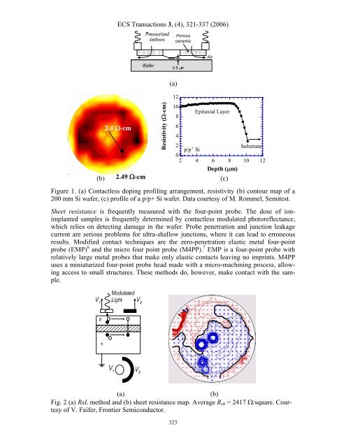
Figure 1. (a) Contactless doping profiling arrangement, resistivity (b) contour map of a<br />
200 mm Si wafer, (c) profile of a p/p+ Si wafer. Data courtesy of M. Rommel, Semitest.<br />
Sheet resistance is frequently measured with the four-point probe. The dose of ionimplanted<br />
samples is frequently determined by contactless modulated photoreflectance,<br />
which relies on detecting damage in the wafer. Probe penetration and junction leakage<br />
current are serious problems for ultra-shallow junctions, where it can lead to erroneous<br />
results. Modified contact techniques are the zero-penetration elastic metal four-point<br />
probe (EMP) 6 and the micro four point probe (M4PP). 7 EMP is a four-point probe with<br />
relatively large metal probes that make only elastic contacts leaving no imprints. M4PP<br />
uses a miniaturized four-point probe head made with a micro-machining process, allowing<br />
access to small structures. These methods do, however, make contact with the sample.<br />
(c)<br />
(a)<br />
(b)<br />
Fig. 2 (a) RsL method and (b) sheet resistance map. Average R sh = 2417 Ω/square. Courtesy<br />
of V. Faifer, Frontier Semiconductor.<br />
323


