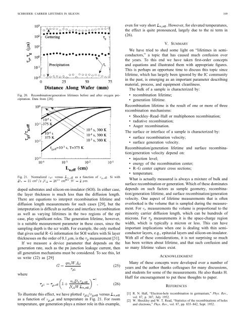
SCHRODER: CARRIER LIFETIMES IN SILICON 169 even for very short However, for elevated temperatures, the effect is quite pronounced, largely due to the ni term <strong>in</strong> (26). Fig. 20. Recomb<strong>in</strong>ation/generation lifetimes before and after oxygen precipitation. Data from [28]. Fig. 21. Normalized g1 versus L n;e as a function of g;e : Si with D n =35cm 2 =s; N A =10 16 cm 03 ;W =2m: doped substrates and silicon-on-<strong>in</strong>sulator (SOI). In either case, the layer thickness is much less than the diffusion length. There are equations to <strong>in</strong>terpret recomb<strong>in</strong>ation lifetime and diffusion length measurements for such cases [29], but the <strong>in</strong>terpretation is difficult as surface and <strong>in</strong>terface recomb<strong>in</strong>ation as well as vary<strong>in</strong>g lifetimes <strong>in</strong> the two regions of the epi case, play significant roles. The generation lifetime, however, is a suitable measurement parameter <strong>in</strong> these cases, s<strong>in</strong>ce the sampl<strong>in</strong>g depth is the scr width. For example, the only method that gives useful R–G <strong>in</strong>formation for SOI wafers with Si layer thicknesses on the order of 0.1 m is the measurement [31]. If we measure a device parameter that depends on the generation rate, such as the pn junction leakage current, then all generation mechanisms must be considered. To see this, let us write (22) as [29] where (25) (26) To illustrate this effect, we have plotted versus as a function of and temperature <strong>in</strong> Fig. 21. For room temperature, qnr generation plays a m<strong>in</strong>or role <strong>in</strong> this example, V. SUMMARY We have tried to shed some light on “lifetimes <strong>in</strong> semiconductors,” a topic that has caused much confusion over the years. To this end we have taken first-order concepts and equations and illustrated them with appropriate figures. This is perhaps an opportune time to discuss this topic s<strong>in</strong>ce lifetime, which has largely been ignored by the IC community <strong>in</strong> the past, is emerg<strong>in</strong>g as an important parameter describ<strong>in</strong>g material, process, and equipment cleanl<strong>in</strong>ess. The bulk of a sample is characterized by: • recomb<strong>in</strong>ation lifetime; • generation lifetime. Recomb<strong>in</strong>ation lifetime is the result of one or more of three recomb<strong>in</strong>ation mechanisms: • Shockley–Read–Hall or multiphonon recomb<strong>in</strong>ation; • radiative recomb<strong>in</strong>ation; • Auger recomb<strong>in</strong>ation. The surface or <strong>in</strong>terface of a sample is characterized by: • surface recomb<strong>in</strong>ation velocity; • surface generation velocity. Recomb<strong>in</strong>ation/generation lifetime and surface recomb<strong>in</strong>ation/generation velocity depend on: • <strong>in</strong>jection level; • energy of the recomb<strong>in</strong>ation center; • R–G center capture cross sections; • temperature. What is actually measured is always a mixture of bulk and surface recomb<strong>in</strong>ation or generation. Which of these dom<strong>in</strong>ates depends on such factors as sample geometry, recomb<strong>in</strong>ation/generation lifetime, and surface recomb<strong>in</strong>ation/generation velocity. One aspect of lifetime measurements that is often overlooked is the volume that is sampled dur<strong>in</strong>g the measurement. For measurements the volume is proportional to the m<strong>in</strong>ority carrier diffusion length, which can be hundreds of microns. For measurements it is the space-charge region width, which is typically a micron or less. This can have important implications when one is deal<strong>in</strong>g with th<strong>in</strong> semiconductor layers, e.g., epitaxial layers and silicon-on-<strong>in</strong>sulator. With all of these considerations, it is not surpris<strong>in</strong>g so much has been written about lifetime, and that such confusion and so many lifetime values exist. ACKNOWLEDGMENT Many of these concepts were developed over a number of years and the author thanks colleagues for many discussions, and students for some of the measurements. He also thanks H. Huff for encouragement to put these thoughts to paper. REFERENCES [1] R. N. Hall, “Electron-hole recomb<strong>in</strong>ation <strong>in</strong> germanium,” Phys. Rev., vol. 87, p. 387, July 1952. [2] W. Shockley and W. T. Read, “Statistics of the recomb<strong>in</strong>ations of holes and electrons,” Phys. Rev., vol. 87, pp. 835–842, Sept. 1952.
170 IEEE TRANSACTIONS ON ELECTRON DEVICES, VOL. 44, NO. 1, JANUARY 1997 [3] R. N. Hall, “Recomb<strong>in</strong>ation processes <strong>in</strong> semiconductors,” Proc. IEE vol. 106B, pp. 923–931, Mar. 1960. [4] D. K. <strong>Schroder</strong>, “The concept of generation and recomb<strong>in</strong>ation lifetimes <strong>in</strong> semiconductors,” IEEE Trans. Electron Devices, vol. ED-29, pp. 1336–1338, Aug. 1982. [5] , Semiconductor Material and Device Characterization. New York: Wiley, 1990, ch. 8. [6] S. K. Pang and A. Rohatgi, “Record high recomb<strong>in</strong>ation lifetime <strong>in</strong> oxidized magnetic Czochralski silicon,” Appl. Phys. Lett., vol. 59, pp. 195–197, July 1991. [7] J. Cornu, R. Sittig, and W. Zimmermann, “Analysis and measurement of carrier lifetimes <strong>in</strong> the various operat<strong>in</strong>g modes of power devices,” Solid-<strong>State</strong> Electron., vol. 17, pp. 1099–1106, Oct. 1974. [8] A. G. Aberle, S. Glunz, and W. Warta, “Impact of illum<strong>in</strong>ation level and oxide parameters on Shockley–Read–Hall recomb<strong>in</strong>ation at the Si- SiO 2 <strong>in</strong>terface,” J. Appl. Phys., vol. 71, pp. 4422–4431, May 1992; S. J. Rob<strong>in</strong>son, S. R. Wenham, P. P. Altermatt, A. G. Aberle, G. Heiser, and M. A. Green, “Recomb<strong>in</strong>ation rate saturation mechanisms at oxidized surfaces of high-efficiency silicon solar cells,” J. Appl. Phys., vol. 78, pp. 4740–4754, Oct. 1995. [9] T. Otaredian, “The <strong>in</strong>fluence of the surface and oxide charge on the surface recomb<strong>in</strong>ation process,” Solid-<strong>State</strong> Electron., vol. 36, pp. 905–915, June 1993. [10] E. O. Johnson, “Large-signal surface photovoltage studies with germanium,” Phys. Rev., vol. 111, pp. 153–166, July 1958. [11] D. J. Fitzgerald and A. S. Grove, “Surface recomb<strong>in</strong>ation <strong>in</strong> semiconductors,” Surf. Sci., vol. 9, pp. 347–369, Feb. 1968. [12] K. L. Luke and L. J. Cheng, “Analysis of the <strong>in</strong>teraction of a laser pulse with a silicon wafer: determ<strong>in</strong>ation of bulk lifetime and surface recomb<strong>in</strong>ation velocity,” J. Appl. Phys., vol. 61, pp. 2282–2293, Mar. 1987. [13] G. Zoth and W. Bergholz, “A fast, preparation-free method to detect iron <strong>in</strong> silicon,” J. Appl. Phys., vol. 67, pp. 6764–6771, June 1990. [14] K. Mishra and R. Falster, Abstr. 426, Electrochem. Soc. Mtg. Extend. Abstr. 92-2, Toronto, Ont, Canada, Oct. 11–16, 1992, p. 632. [15] O. J. Antilla and M. V. Tilli, “Metal contam<strong>in</strong>ation removal on silicon wafers us<strong>in</strong>g dilute acidic solutions,” J. Electrochem. Soc., vol. 139, pp. 1751–1756, June 1992. [16] Y. Kitagawara, T. Yoshida, T. Hamaguchi, and T. Takenaka, “Evaluation of oxygen-related carrier recomb<strong>in</strong>ation centers <strong>in</strong> high-purity Czochralski-grown Si crystals by the bulk lifetime measurements,” J. Electrochem. Soc., vol. 142, pp. 3505–3509, Oct. 1995. [17] M. Miyazaki, S. Miyazaki, T. Kitamura, T. Aoki, Y. Nakashima, M. Hourai, and T. Shigematsu, “Influence of Fe contam<strong>in</strong>ation <strong>in</strong> Czochralski-grown silicon s<strong>in</strong>gle crystals on LSI-yield related crystal quality characteristics,” Jpn. J. Appl. Phys., vol. 34, pp. 409–413, Feb. 1995. [18] A. L. P. Rotondero, T. Q. Hurd, A. Kaniara, J. Vanhellemont, E. Simoen, M. M. Heyns, and C. Claeys, “Impact of Fe and Cu contam<strong>in</strong>ation on the m<strong>in</strong>ority carrier lifetime of silicon substrates,” J. Electrochem. Soc., vol. 143, pp. 3014–3019, Sept. 1996. [19] S. K. Pang and A. Rohatgi, “A new methodology for separat<strong>in</strong>g Shockley–Read–Hall lifetime and Auger recomb<strong>in</strong>ation coefficients from the photoconductivity decay technique,” J. Appl. Phys., vol. 74, pp. 5554–5560, Nov. 1993. [20] T. Maekawa and K. Fujiwara, “Measurable range of bulk carrier lifetime for a thick silicon wafer by <strong>in</strong>duced eddy current method,” Jpn. J. Appl. Phys., vol. 35, pp. 3955–3964, Aug. 1995. [21] E. Yablanovitch, R. M. Swanson, W. D. Eades, and B. R. We<strong>in</strong>berger, “Electron-hole recomb<strong>in</strong>ation at the Si-SiO 2 <strong>in</strong>terface,” Appl. Phys. Lett., vol. 48, pp. 245–247, Jan. 1986. [22] E. Yablanovitch, D. L. Allara, C. C, Chang, T. Gmitter, and T. B. Bright, “Unusually low surface-recomb<strong>in</strong>ation velocity on silicon and germanium surfaces,” Phys. Rev. Lett., vol. 57, pp. 249–252, July 1986. [23] H. M’saad, J. Michel, J. J. Lappe, and L. C. Kimerl<strong>in</strong>g, “Electronic passivation of silicon surfaces by halogens,” J. Electron. Mat., vol. 23, pp. 487–491, May 1994. [24] H. M’saad, J. Michel, A. Reddy, and L. C. Kimerl<strong>in</strong>g, “Monitor<strong>in</strong>g and optimization of silicon surface quality,” J. Electrochem. Soc., vol. 142, pp. 2833–2835, Aug. 1995. [25] J. Lagowski, A. M. Kontkiewicz, L. Jastrzebski, and P. Edelman, “Method for the measurement of long m<strong>in</strong>ority carrier diffusion lengths exceed<strong>in</strong>g wafer thickness,” Appl. Phys. Lett., vol. 63, pp. 2902–2904, Nov. 1993. [26] A. Buczkowski, G. Rozgonyi, and F. Shimura, “Photoconductance m<strong>in</strong>ority carrier lifetime versus surface photovoltage diffusion length <strong>in</strong> silicon,” J. Electrochem. Soc., vol. 140, pp. 3240–3245, Nov. 1993. [27] D. K. <strong>Schroder</strong>, J. D. Whitfield, and C. J. Varker, “Recomb<strong>in</strong>ation lifetime us<strong>in</strong>g the pulsed MOS capacitor,” IEEE Trans. Electron Devices, vol. ED-31, pp. 463–467, Apr. 1984. [28] D. K. <strong>Schroder</strong>, J. M. Hwang, J. S. Kang, A. M. Goodman and B. L. Sopori, “Lifetime and recomb<strong>in</strong>ation concepts for oxygen-precipitated silicon,” <strong>in</strong> VLSI Science and Technology/1985, M. Bullis and S. Broydo, Eds. Penn<strong>in</strong>gton, NJ: Electrochemical Society, May 1985, pp. 419–428. [29] D. K. <strong>Schroder</strong>, “Effective lifetimes <strong>in</strong> high-quality silicon devices,” Solid-<strong>State</strong> Electron., vol. 27, pp. 247–251, Mar. 1984. [30] A. Ohsawa, K. Honda, R. Takizawa, T. Nakanishi, M. Aoki, and N. Toyokura, “Effects of impurities on microelectronic devices,” <strong>in</strong> Semiconductor <strong>Silicon</strong> 1990, H. R. Huff, K. G. Barraclough, and J. I. Chikawa, Eds. Penn<strong>in</strong>gton, NJ: Electrochemical Society, 1990, pp. 601–613. [31] D. E. Ioannou, S. Cristoloveanu, M. Mukherjee, and B. Mazhari, “Characterization of carrier generation <strong>in</strong> enhancement-mode SOI MOS- FET’s,” IEEE Electron Device Lett., vol. 11, pp. 409–411, Sept. 1990. <strong>Dieter</strong> K. <strong>Schroder</strong> (S’61–M’67–SM’78–F’96) received the B.S. and M.S. degrees <strong>in</strong> 1962 and 1964, from McGill <strong>University</strong>, Montreal, P.Q., Canada, and the Ph.D. degree from the <strong>University</strong> of Ill<strong>in</strong>ois, Urbana-Champaign, <strong>in</strong> 1968. In 1968, he jo<strong>in</strong>ed the West<strong>in</strong>ghouse Research Labs, where he was engaged <strong>in</strong> reserach on various aspects of semiconductor devices, <strong>in</strong>clud<strong>in</strong>g MOS devices, imag<strong>in</strong>g arrays, power devices, and magnetostatic waves. He spent a year at the Institute of Applied Solid <strong>State</strong> Physics, Germany, <strong>in</strong> 1978. In 1981, he jo<strong>in</strong>ed the Center for Solid <strong>State</strong> Electronics Research, <strong>Arizona</strong> <strong>State</strong> <strong>University</strong>, Tempe. His current <strong>in</strong>terests are semiconductor materials and devices, characerization, low-power electronics, and defects <strong>in</strong> semiconductors. He has written two books Advanced MOS Devices and Semiconductor Material and Device Characterization, (New York: Wiley, 1990) and has published over 100 papers. Dr. <strong>Schroder</strong> was a Dist<strong>in</strong>guished National Lecturer, IEEE Electron Devices Society, <strong>in</strong> 1993 and 1994.