

Surface voltage and surface photovoltage - Dieter Schroder ...
Surface voltage and surface photovoltage - Dieter Schroder ...
Surface voltage and surface photovoltage - Dieter Schroder ...

Create successful ePaper yourself
Turn your PDF publications into a flip-book with our unique Google optimized e-Paper software.
<strong>Surface</strong> <strong>voltage</strong> <strong>and</strong> <strong>surface</strong> photo<strong>voltage</strong><br />
R<br />
Φ(λ)<br />
s 1 s 2<br />
p-Type<br />
τ, D, L<br />
0 d x<br />
(a)<br />
R<br />
Φ(λ)<br />
s 1 s 2<br />
p-Type<br />
τ, D, L<br />
∆n(W)<br />
0 W d x<br />
(b)<br />
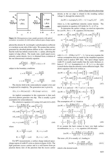
Figure A1. Homogeneous p-type sample geometry with optical<br />
excitation: (a) neutral, (b) with <strong>surface</strong>-induced space-charge region.<br />
photon flux density , wavelength λ <strong>and</strong> absorption coefficient<br />
α is incident on one side of this wafer. We assume that carriers<br />
generated by absorbed photons diffuse in the x-direction <strong>and</strong><br />
that the wafer has infinite extent in the y–z-plane, allowing the<br />
neglect of edge effects. The steady state, small-signal excess<br />
minority carrier density n(x) is obtained from a solution of<br />
the one-dimensional continuity equation<br />
D d2 n(x)<br />
dx 2<br />
− n(x)<br />
τ<br />
subject to the boundary conditions<br />
+ G(x) = 0 (A1)<br />
x = 0: dn(x) n(0)<br />
= s 1<br />
dx x=0 D<br />
<strong>and</strong><br />
x = d: dn(x) n(d)<br />
=−s 2<br />
dx x=d D . (A2)<br />
The electric field in the semiconductor sample is low <strong>and</strong><br />
is neglected for simplicity. The generation rate is given by<br />
G(x, λ) = (λ)α(λ)[1 − R(λ)]exp(−α(λ)x).<br />
(A3)<br />
An implicit assumption in this expression is that each<br />
absorbed photon generates one ehp. This is usually a good<br />
assumption for semiconductors.<br />
The solution to equation (A1) using (A2) <strong>and</strong> (A3) is [62]<br />
{[ ( )<br />
(1 − R)ατ<br />
d − x<br />
n(x) = K<br />
(α 2 L 2 1 sinh<br />
− 1)<br />
L<br />
( ) [ ( d − x<br />
x<br />
+K 2 cosh +e −αd K 3 sinh<br />
L<br />
L)<br />
( )]][( x s1 s 2 L<br />
+K 4 cosh<br />
L D<br />
+ D ) ( d<br />
sinh<br />
L L)<br />
( d −1 }<br />
+(s 1 + s 2 ) cosh − e<br />
L)] −αx (A4)<br />
where<br />
K 1 = s 1s 2 L<br />
D + s 2αL K 2 = s 1 + αD<br />
K 3 = s 1s 2 L<br />
D − s 1αL K 4 = s 2 − αD.<br />
For SPV measurements, a <strong>surface</strong> charge induced spacecharge<br />
region of width W exists as shown in figure A1(b). The<br />
light generates excess carriers <strong>and</strong> it is well known from pn<br />
junction theory (law of the junction) that the excess carrier<br />
density at the scr edge is related to the resulting <strong>surface</strong><br />
<strong>voltage</strong> V S through the relation [25]<br />
n(W) = n 0 (exp(qV S /kT) − 1) ≈ n 0 qV S /kT<br />
(A5)<br />
where n 0 is the equilibrium minority carrier density. The<br />
approximation in equation (A5) holds for V S ≪ kT/q.<br />
To determine the <strong>surface</strong> <strong>voltage</strong>, we need an expression<br />
for n(W). Forx = W, equation (A4) becomes<br />
{[ ( ) ( )<br />
d − W<br />
d − W<br />
n(W) = A K 1 sinh + K 2 cosh<br />
L<br />
L<br />
( ) ( )]]<br />
W W<br />
+e<br />
[K −αd 3 sinh + K 4 cosh<br />
L L<br />
[(<br />
s1 s 2 L<br />
×<br />
D<br />
+ D ) ( ( d d −1<br />
sinh + (s 1 + s 2 ) cosh<br />
L L)<br />
L)]<br />
}<br />
−e −αW (A6)<br />
with A = (1 − R)ατ/(α 2 L 2 − 1). Let us now examine the<br />
various assumptions that are made for the simplified equation<br />
usually used to analyse SPV data. The space-charge region<br />
width W is usually much smaller than the wafer thickness d,<br />
hence d −W ≈ d. Assumption (i): d −W ≫ L, i.e., the wafer<br />
is much thicker than the minority carrier diffusion length. This<br />
allows equation (A6) to be written as<br />
{[ [ ( ) ( )]<br />
W W<br />
n(W) = A (K 1 + K 2 ) cosh − sinh<br />
L L<br />
( ) ( )]/ ]<br />
W W<br />
+e<br />
[K −αd 3 sinh + K 4 cosh cosh(d/L)<br />
L L<br />
[<br />
s1 s 2 L<br />
×<br />
D + D ] −1 }<br />
L + s 1 + s 2 − e −αW . (A7)<br />
For W ≪ L <strong>and</strong> α(d − W) ≈ αd ≫ 1, we have<br />
{( [<br />
(1 − R)ατ<br />
n(W) = (K<br />
(α 2 L 2 1 + K 2 ) 1 − W ])<br />
− 1)<br />
L<br />
(<br />
s1 s 2 L<br />
×<br />
D + D ) −1 }<br />
L + s 1 + s 2 − e −αW . (A8)<br />
The assumption αW ≪ 1 leads to<br />
{[(<br />
(1 − R)αL<br />
n(W) = s<br />
(α 2 L 2 2 + D ) (<br />
(αL − 1) 1+ s )]<br />
1W<br />
− 1) L<br />
D<br />
[<br />
× s 2 s 1 + D ( )] D −1 }<br />
L L + s 1 + s 2<br />
{[(<br />
(1 − R)αL<br />
= 1+ D )(<br />
1+ s )]<br />
1W<br />
(αL +1) s 2 L D<br />
[<br />
× s 1 + D (<br />
1+ D<br />
L s 2 L + s )] −1 }<br />
1<br />
. (A9)<br />
s 2<br />
If we assume the back contact to have very high <strong>surface</strong><br />
recombination, i.e., s 2 →∞, equation (A9) becomes<br />
n(W) =<br />
(1 − R)αL<br />
(αL +1)<br />
( 1+s1 W/D<br />
s 1 + D/L<br />
The term s 1 W/D is usually ≪1, leading to<br />
(1 − R) αL<br />
n(W) =<br />
(s 1 + D/L) (1+αL)<br />
which is the desired result.<br />
)<br />
. (A10)<br />
(A11)<br />
R29


