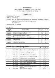
LAB 7: AMPLITUDE MODULATION USING PSPICE OBJECTIVE: In ...
LAB 7: AMPLITUDE MODULATION USING PSPICE OBJECTIVE: In ...
LAB 7: AMPLITUDE MODULATION USING PSPICE OBJECTIVE: In ...

Create successful ePaper yourself
Turn your PDF publications into a flip-book with our unique Google optimized e-Paper software.
<strong>LAB</strong> 7: <strong>AMPLITUDE</strong> <strong>MODULATION</strong> <strong>USING</strong> <strong>PSPICE</strong><br />
<strong>OBJECTIVE</strong>:<br />
<strong>In</strong> this lab, you will learn how to perform amplitude modulation of message signal using<br />
<strong>PSPICE</strong> and MAT<strong>LAB</strong> simulation and to calculate the modulation index for various levels of<br />
modulating voltages.<br />
SOFTWARE REQUIRED:<br />
1. ORCAD 9.2<br />
2. MAT<strong>LAB</strong> 7.0<br />
PRE-<strong>LAB</strong>:<br />
Write the netlist for the given AM circuit and plot the modulating signal, carrier signal<br />
and AM signal using PROBE function using <strong>PSPICE</strong> . Find the modulating index for the<br />
modulating voltage of 4V. Assume carrier voltage as 50mV, carrier frequency is 5KHz and<br />
modulating frequency is 1KHz.<br />
PART – 1<br />
ABOUT <strong>PSPICE</strong>:<br />
SPICE is a general purpose circuit program that can be applied to stimulate and calculate<br />
the performance of electrical and electronic circuits.<br />
A circuit is described to a computer by using a file called circuit file. The circuit file<br />
contains the circuit details of component and elements, ht information about the sources and the<br />
commands for what to calculate and what to provide as output. The circuit file is the input file to<br />
the SPICE program, which after executing the commands, produces the result in another file<br />
called output file.<br />
The description of analysis of a circuit require specifying the following:<br />
Element values<br />
Nodes<br />
Circuit elements<br />
Element modes<br />
Sources<br />
Types of analysis<br />
Output variables<br />
<strong>PSPICE</strong> output commands<br />
Format of output files<br />
Format of circuit files
Element values:<br />
The elements values are written in standard floating point notation with optimal scale and<br />
unit suffixs<br />
Ex: V=Volt, A=Ampere, Hz= Hertz, OHM= ohm<br />
Node voltage:<br />
The voltage of a point with respect to ground references point.<br />
Vname +node -node Value<br />
Ex: Vcc 1 0 30v<br />
The passive component is also indicated as<br />
Rname +node -node Values<br />
R1 2 3 10k<br />
Format of circuit files:<br />
Title<br />
The circuit file that can be read by <strong>PSPICE</strong> may be divided into 5 parts<br />
Circuit description<br />
Analysis description<br />
Output description<br />
.END ( end of statement)<br />
Notes:<br />
1. The first line is the title line and it may contain any type of text.<br />
2. The last line must be the .END command.<br />
3. The order of the remaining lines is not important and does not affect the results of<br />
simulations.<br />
4. If the statement is more than one line, the statements can continue on the next line. A<br />
continuation line is identified by a plus sign(+) in the first column of the next line<br />
5. The comment line may be included anywhere, precede by an asterisk (*). Within a<br />
statement. A comment is preceded by a semicolon (;).
6. The number of blanks between items is not significant. The tabs and commas are<br />
equivalent to blanks. The tabs and commas are equivalent.<br />
7. The statement or comments can be in either lower case or upper case.<br />
8. If you are not sure of any command or statement, the best thing is to run the circuit file by<br />
using that command or statement and see what happened. <strong>PSPICE</strong> is user friendly<br />
software; it gives an error message in the output file that identifies a problem.<br />
PRINT statement<br />
.Print dc [output variables]<br />
The print statement used to get the DC outputs. The maximum number of output<br />
variables is 8. .Print statement can be used to print all the desired output variables. The values of<br />
the output variables are printed as a table with each column corresponding to one output variable.<br />
PLOT statement:<br />
The result from dc analysis van also be obtained in the form of line printer plots. The<br />
plots are drawn by suing characters.<br />
.plot dc<br />
+[ ]<br />
The plot statement can be used to plot all the desired output variables.<br />
PROBE Statement:<br />
Probe is a graphics post processor/ waveform analyser for<strong>PSPICE</strong>.<br />
.probe<br />
.probe < one or more output variables><br />
<strong>In</strong> the first form no output variables is specified, the .probe command writes all the node<br />
voltages and all the element currents in to the probe.dat file. <strong>In</strong> the second form where the output<br />
variables are specified, only the specified output variables to the probe.dat file.<br />
Run the program by typing filename.cir which should place you in probe with an empty screen<br />
and a message saying that “ all voltages and currents are available”. That is, data for all node<br />
voltages and element currents in the circuit have been passed from pspice to probe<br />
Select Add_Trace. Functional graphs are called “traces” by probe. At this point type the<br />
names of variables to be traced. Push ENTER to get the trace. Notice that both axes are<br />
cutomatically scaled to suit the curve.
The Zoom feature of probe displays is very useful if you are interested in an small region<br />
of the highlighted. The Zoom in on the peak of the power curve, select Zoom, and select Specify<br />
region which is highlighted.<br />
The cursor feature of probe is very useful to find maxima or minima values. Select<br />
Cursor to go to the cursor submenu.<br />
Once the results of the simulations are processed by the .probe command the result are<br />
available for graphical displays.<br />
Tran statement:<br />
Transient analysis can be performed by the .Tran command<br />
.tran[/op] print_step end_time (no_print_time [step_ceiling]) [UIC]<br />
/op = to print detailed information about the transient analysis operating point<br />
Print_step = it specifies the time increment between the results which are printed in tabular form<br />
into the output file.<br />
End_time = it specifies the final time of the transient calculation.<br />
No_print_time = it specifies a value of time, before which results will not be printed to probe for<br />
graphing.<br />
Step_ceiling = it is the maximum time interval used by the pspice in its internal calculations<br />
which is default by end time/50.<br />
UIC = directs pspice to use initial conditions given to inductors and capacitors in their defininf L<br />
or C statement.<br />
Ac source:<br />
The general transient analysis for SIN is<br />
Sin (offset amplitude freq delay damping factor phase)<br />
Frequency response:<br />
.ac sweeptype points fstart fstop<br />
Sweeptype = LIN,DEC,OCT<br />
Fstart = starting frequency must specified in Hz. They also must be positive.<br />
Fstop = ending frequency must specified in Hz. They also must be positive.
Points = it specifies the number of calculations for every power of ten in the frequency range.<br />
Transfer function:<br />
It can be used to compute the small signal dc gain, the input resistance and the output<br />
resistance of a circuit.<br />
.Tf<br />
Vout Vin<br />
.Tf Iout Iin<br />
The .tf command calculates the parameters of Thevenin’s and Norton equivalent circuit for the<br />
circuit file.It automatically prints the output and does not require .print,.plot or .probe statement.<br />
Dc sweep:<br />
The Dc sweep is also known as dc transfer characteristics. The input variable is varied<br />
over a range of values. For each value of the input variable. The dc operating and the small<br />
signal dc gain are computed by calling the small signal transfer function.<br />
.dc LIN swname sstart send sinc<br />
.dc oct swname sstart send np<br />
.dc DEC swname sstart send np<br />
.dc swname list <br />
Swname = sweep variable name may be V orI<br />
Sstart = start value<br />
Send = end value<br />
Sinc = increment value of the sweep variable. It should be positive.<br />
Np = number of steps.<br />
.Lib statement:<br />
A library file may be referenced in the circuit file by using the following statement.<br />
.lib fname<br />
Fname = name of the library file.
A library file may contain comments, .model statements, sub circuit definition, .lib<br />
statements and .end statements. No other statements are permitted. If fname is omitted, pspice<br />
looks for the default file EVAL.LIB.<br />
When a .lib command calls for a file, it does not bring the whole text of the library file<br />
into the circuit file. It simply reads those models or sub circuits that are called by the main circuit<br />
file.<br />
DESIGN AND PROCEDURE:<br />
Circuit diagram<br />
NETLIST:<br />
VIN 1 0 AC 10MV SIN(0 10MV 1KHZ )<br />
VCC 7 0 DC 15V<br />
RS 1 2 500<br />
R1 7 3 47K<br />
R2 3 0 5K<br />
RC 7 4 10K
RE 5 0 2K<br />
RL 6 0 20K<br />
C1 2 3 1UF<br />
C2 4 6 1UF<br />
CE 5 0 10UF<br />
Q1 4 3 5 Q2N2222<br />
plot the results of transient analysis for voltages at nodes 4,6 & 1<br />
.PLOT TRAN V(4) V(6) V(1)<br />
Plot the results of the ac analysis for the magnitude and phase angle<br />
.PLOT AC VM(6) VP(6)<br />
Print details of transient analysis operating point<br />
.TRAN/OP 50US 2MS<br />
Ac analysis from 1hz to 10khz with a decade increment and to points per decade<br />
.AC DEC 10 1HZ 10KHZ<br />
Generate the graphical plots in the output file<br />
.PROBE<br />
.END<br />
Test procedure:<br />
1. Open the Pspice AD Lite software by double clicking its icon.<br />
2. After few moments Command window will appear.<br />
3. Go to the File Menu and select a New text file. (File Newtext file)<br />
4. A blank text file will appear with a title ‘untitled’<br />
5. Now start typing your program. After completing, save the text file as .cir with appropriate<br />
name. To execute the program go to Debug Menu and select Run.<br />
6. After execution output will appear in the Command window .If there is an error then with an<br />
alarm, type of error will appear .<br />
7. If the results contain errors, start up the text editing program again and modify the netlist.<br />
8. Rectify the error if any and go to Debug Menu and select Run.
9. If there is no error go to Trace menu and click add trace. Enter the output node voltage and<br />
click ok then the output will displayed.<br />
<strong>LAB</strong> RESULT:<br />
Thus the netlist for the given AM circuit was written and the output waveforms were<br />
plotted using probe statements.<br />
QUESTION:<br />
1. What is the difference of plotting the output using TRAN and AC?<br />
2. Which statement is used to get more than one plot?<br />
3. How much power is transmitted if the modulation index of an AM wave is changed from<br />
0 to 1.<br />
4. Which type of modulation is used in TV transmission? Jusity it.<br />
5. How many AM broadcast stations that can be accommodated in a 100KHz bandwidth for<br />
the highest modulating frequency of 5KHz?<br />
ASSESSMENT:<br />
PRE<strong>LAB</strong><br />
: 30 Pts<br />
(circuit(10), program(20))<br />
<strong>LAB</strong> PERFORMANCE<br />
VIVA<br />
: 30 Pts<br />
: 15 Pts
<strong>LAB</strong> 8: FREQUENCY <strong>MODULATION</strong> <strong>USING</strong> <strong>PSPICE</strong> AND MAT<strong>LAB</strong><br />
<strong>OBJECTIVE</strong>:<br />
<strong>In</strong> this lab, you will learn how to perform frequency modulation of message signal using<br />
<strong>PSPICE</strong> and MAT<strong>LAB</strong> simulation and to calculate the modulation index for various levels of<br />
modulating voltages.<br />
SOFTWARE REQUIRED:<br />
1. ORCAD 9.2<br />
2. MAT<strong>LAB</strong> 7.0<br />
PRE-<strong>LAB</strong>:<br />
Write the netlist for the given FM circuit and plot the modulating signal, carrier signal<br />
and FM signal using PROBE function using <strong>PSPICE</strong> . Find the modulating index for the<br />
modulating voltage of 4V. Assume carrier voltage as 50mV, carrier frequency is 5KHz and<br />
modulating frequency is 1KHz.<br />
PART – 1<br />
ABOUT <strong>PSPICE</strong>:<br />
Refer Lab V.<br />
DESIGN AND PROCEDURE:<br />
Circuit Diagram:<br />
Refer Lab II.<br />
Test procedure:<br />
1. Open the Pspice AD Lite software by double clicking its icon.<br />
2. After few moments Command window will appear.<br />
3. Go to the File Menu and select a New text file. (File Newtext file)<br />
4. A blank text file will appear with a title ‘untitled’<br />
5. Now start typing your program. After completing, save the text file as .cir with appropriate<br />
name. To execute the program go to Debug Menu and select Run.<br />
6. After execution output will appear in the Command window .If there is an error then with an<br />
alarm, type of error will appear .
7. Rectify the error if any and go to Debug Menu and select Run.<br />
8. If there is no error go to Trace menu and click add trace. Enter the output node voltage and<br />
click ok then the output will displayed.<br />
<strong>LAB</strong> RESULT:<br />
Thus the netlist for the given FM circuit was written and the output waveforms were<br />
plotted using probe statements.<br />
QUESTION:<br />
1. How can you change the title in the plot?<br />
2. What will be the change in the bandwidth if modulating frequency is doubled?<br />
3. For the modulating signal of 15KHz, find the maximum possible number of channels<br />
available in VHF band. Compare it with the number of channels in MF band(300KHz –<br />
3MHz) band gap between the channels is 0.<br />
4. The narrow band FM has no amplitude variation, inspite of the fact that is has frequency<br />
component as AM. Justify the statement with the help of phasor diagram.<br />
5. What is the difference between plot and probe statement?<br />
ASSESSMENT:<br />
PRE<strong>LAB</strong><br />
: 30 Pts<br />
(circuit(10), program(20))<br />
<strong>LAB</strong> PERFORMANCE<br />
VIVA<br />
: 30 Pts<br />
: 15 Pts
<strong>LAB</strong> 9: PULSE <strong>AMPLITUDE</strong> <strong>MODULATION</strong> AND DE<strong>MODULATION</strong> <strong>USING</strong> <strong>PSPICE</strong><br />
<strong>OBJECTIVE</strong>:<br />
<strong>In</strong> this lab, you will learn how to perform pulse amplitude modulation and demodulation<br />
of message signal using <strong>PSPICE</strong> simulation and tofind the pulse amplitude modulation voltages.<br />
SOFTWARE REQUIRED:<br />
1. ORCAD 9.2<br />
PRE-<strong>LAB</strong>:<br />
Write the netlist for the given PAM circuit and plot the modulating signal, carrier signal<br />
and PAM signal using PROBE function using <strong>PSPICE</strong> . Find the pulse amplitude modulating<br />
voltage for the modulating voltage of 4V. Assume carrier voltage as 4V, carrier frequency is<br />
6KHz and modulating frequency is 1KHz.<br />
PART – 1<br />
ABOUT <strong>PSPICE</strong>:<br />
Refer Lab V.<br />
DESIGN AND PROCEDURE:<br />
Circuit Diagram:<br />
Refer Lab III.<br />
Test procedure:<br />
1. Open the Pspice AD Lite software by double clicking its icon.<br />
2. After few moments Command window will appear.<br />
3. Go to the File Menu and select a New text file. (File Newtext file)<br />
4. A blank text file will appear with a title ‘untitled’<br />
5. Now start typing your program. After completing, save the text file as .cir with appropriate<br />
name. To execute the program go to Debug Menu and select Run.<br />
6. After execution output will appear in the Command window .If there is an error then with an<br />
alarm, type of error will appear .<br />
7. Rectify the error if any and go to Debug Menu and select Run.
8. If there is no error go to Trace menu and click add trace. Enter the output node voltage and<br />
click ok then the output will displayed.<br />
RESULT:<br />
Thus the netlist for the given pulse amplitude modulation and demodulation circuit was<br />
written and the output waveforms were plotted using probe statements.<br />
QUESTION:<br />
1. How to add the text in the plot?<br />
2. How to add the text in the plot?<br />
3. Bandwidth of the PAM signal is 2nfm. Justify.<br />
4. <strong>In</strong> the present day standard digital voice communication, the amplitude of the voice<br />
signal is sampled at what rate?<br />
5. what is the maximum permissible distance between 2 samples of a 2KHz signal?<br />
ASSESSMENT:<br />
PRE<strong>LAB</strong><br />
: 30 Pts<br />
(circuit(10), program(20))<br />
<strong>LAB</strong> PERFORMANCE<br />
VIVA<br />
: 30 Pts<br />
: 15 Pts
<strong>LAB</strong> 10: PRE-EMPHASIS AND DE-EMPHASIS <strong>USING</strong> <strong>PSPICE</strong><br />
<strong>OBJECTIVE</strong>:<br />
<strong>In</strong> this lab, you will learn how to perform pre-emphasis and de-emphasisl using <strong>PSPICE</strong><br />
simulation and tofind the cut off frequency.<br />
SOFTWARE REQUIRED:<br />
1. ORCAD 9.2<br />
PRE-<strong>LAB</strong>:<br />
Write the netlist for the given pre-emphasis and de-emphasis circuit and plot the<br />
frequency response curve using PROBE function using <strong>PSPICE</strong> . Find the cut off frequency.<br />
PART – 1<br />
ABOUT <strong>PSPICE</strong>:<br />
Refer Lab V.<br />
DESIGN AND PROCEDURE:<br />
Circuit Diagram:<br />
Refer Lab IV.<br />
Test procedure:<br />
1. Open the Pspice AD Lite software by double clicking its icon.<br />
2. After few moments Command window will appear.<br />
3. Go to the File Menu and select a New text file. (File Newtext file)<br />
4. A blank text file will appear with a title ‘untitled’<br />
5. Now start typing your program. After completing, save the text file as .cir with appropriate<br />
name. To execute the program go to Debug Menu and select Run.<br />
6. After execution output will appear in the Command window .If there is an error then with an<br />
alarm, type of error will appear .<br />
7. Rectify the error if any and go to Debug Menu and select Run.<br />
8. If there is no error go to Trace menu and click add trace. Enter the output node voltage and<br />
click ok then the output will displayed.
<strong>LAB</strong> RESULT:<br />
Thus the netlist for the given pre-emphasis and de-emphasis circuit was written and the<br />
output waveforms were plotted using probe statements.<br />
QUESTION:<br />
1. How to include the file in the circuit file?<br />
2. How to add the arrows in the plot?<br />
3. What is the effect of the threshold in signal to noise ratio at the detector?<br />
4. How to include a device which is not already existed in pspice library?<br />
5. <strong>In</strong> a commercial FM broadcast system, the modulating signal frequency is limited to what<br />
frequency?<br />
ASSESSMENT:<br />
PRE<strong>LAB</strong><br />
: 30 Pts<br />
(circuit(10), program(20))<br />
<strong>LAB</strong> PERFORMANCE<br />
VIVA<br />
: 30 Pts<br />
: 15 Pts