RD06HVF1 - RFPhone
RD06HVF1 - RFPhone
RD06HVF1 - RFPhone

You also want an ePaper? Increase the reach of your titles
YUMPU automatically turns print PDFs into web optimized ePapers that Google loves.
ELECTROSTATIC SENSITIVE DEVICE<br />
OBSERVE HANDLING PRECAUTIONS<br />
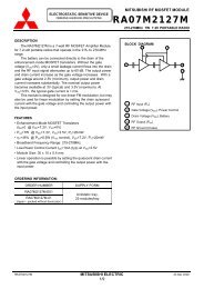
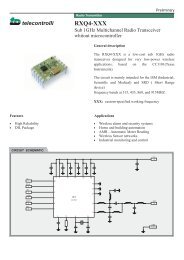
MITSUBISHI RF POWER MOS FET<br />
<strong>RD06HVF1</strong><br />
RoHS Compliance, Silicon MOSFET Power Transistor 175MHz,6W<br />
ABSOLUTE MAXIMUM RATINGS<br />
(Tc=25°C UNLESS OTHERWISE NOTED)<br />
SYMBOL PARAMETER CONDITIONS RATINGS UNIT<br />
VDSS Drain to source voltage Vgs=0V 50 V<br />
VGSS Gate to source voltage Vds=0V +/- 20 V<br />
Pch Channel dissipation Tc=25°C 27.8 W<br />
Pin Input power Zg=Zl=50Ω 0.6 W<br />
ID Drain current - 3 A<br />
Tch Channel temperature - 150 °C<br />
Tstg Storage temperature - -40 to +150 °C<br />
Rth j-c Thermal resistance junction to case 4.5 °C/W<br />
Note 1: Above parameters are guaranteed independently.<br />
ELECTRICAL CHARACTERISTICS<br />
(Tc=25°C, UNLESS OTHERWISE NOTED)<br />
SYMBOL PARAMETER CONDITIONS<br />
LIMITS UNIT<br />
MIN TYP MAX.<br />
IDSS Zero gate voltage drain current VDS=17V, VGS=0V - - 10 uA<br />
IGSS Gate to source leak current VGS=10V, VDS=0V - - 1 uA<br />
VTH Gate threshold Voltage VDS=12V, IDS=1mA 1.9 - 4.9 V<br />
Pout Output power VDD=12.5V, Pin=0.3W, 6 10 - W<br />
ηD Drain efficiency f=175MHz, Idq=0.3A 60 65 - %<br />
Load VSWR tolerance VDD=15.2V,Po=6W(Pin Control)<br />
f=175MHz,Idq=0.3A,Zg=50Ω<br />
Load VSWR=20:1(All Phase)<br />
No destroy -<br />
Note : Above parameters , ratings , limits and conditions are subject to change.<br />
<strong>RD06HVF1</strong> MITSUBISHI ELECTRIC 10 Jan 2006<br />
2/8