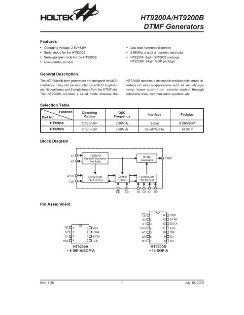
HT9200A/HT9200B DTMF Generators - RFPhone
HT9200A/HT9200B DTMF Generators - RFPhone
HT9200A/HT9200B DTMF Generators - RFPhone

Create successful ePaper yourself
Turn your PDF publications into a flip-book with our unique Google optimized e-Paper software.
<strong>HT9200A</strong>/<strong>HT9200B</strong><br />
<strong>DTMF</strong> <strong>Generators</strong><br />
Features<br />
<br />
Operating voltage: 2.5V~5.5V<br />
<br />
Low total harmonic distortion<br />
<br />
Serial mode for the <strong>HT9200A</strong><br />
<br />
3.58MHz crystal or ceramic resonator<br />
<br />
<br />
Serial/parallel mode for the <strong>HT9200B</strong><br />
Low standby current<br />
<br />
<strong>HT9200A</strong>: 8-pin DIP/SOP package<br />
<strong>HT9200B</strong>: 14-pin SOP package<br />
General Description<br />
The <strong>HT9200A</strong>/B tone generators are designed for MCU<br />
interfaces. They can be instructed by a MCU to generate<br />
16 dual tones and 8 single tones from the <strong>DTMF</strong> pin.<br />
The <strong>HT9200A</strong> provides a serial mode whereas the<br />
<strong>HT9200B</strong> contains a selectable serial/parallel mode interface<br />
for various applications such as security systems,<br />
home automation, remote control through<br />
telephone lines, communication systems, etc.<br />
Selection Table<br />
Part No.<br />
Function<br />
Operating<br />
Voltage<br />
OSC<br />
Frequency<br />
Interface<br />
Package<br />
<strong>HT9200A</strong> 2.5V~5.5V 3.58MHz Serial 8 DIP/SOP<br />
<strong>HT9200B</strong> 2.5V~5.5V 3.58MHz Serial/Parallel 14 SOP<br />
Block Diagram<br />
: <br />
:<br />
! # & 0 <br />
+ HO I J= 4 A I = J H<br />
I ? E= J H<br />
, 6 .<br />
/ A A H= J H<br />
, 6 .<br />
, ) 6 )<br />
+ <br />
5 A HE= , = J=<br />
1 F K J+ EH? K EJ<br />
+ JH <br />
+ EH? K EJ<br />
2 = H= A , = J=<br />
1 F K J+ EH? K EJ<br />
+ - 5 2 , ! , , , <br />
Pin Assignment<br />
+ -<br />
<br />
"<br />
8 , ,<br />
:<br />
!<br />
, 6 .<br />
+ -<br />
:<br />
: <br />
8 5 5<br />
<br />
!<br />
"<br />
&<br />
%<br />
$<br />
#<br />
8 , ,<br />
, 6 .<br />
, ) 6 )<br />
+ <br />
: <br />
8 5 5<br />
+<br />
, <br />
, <br />
!<br />
"<br />
#<br />
$<br />
%<br />
<br />
<br />
<br />
'<br />
&<br />
, ) 6 )<br />
+ <br />
5 2<br />
, !<br />
,<br />
0 6 ' )<br />
& , 12 ) 5 2 )<br />
0 6 ' *<br />
" 5 2 )<br />
Rev. 1.30 1 July 18, 2003
<strong>HT9200A</strong>/<strong>HT9200B</strong><br />
Pad Assignment Pad Coordinates Unit: m<br />
:<br />
: <br />
8 5 5<br />
, <br />
Chip size: 1460 1470 (m) 2<br />
Pad<br />
No.<br />
X<br />
Y<br />
Pad<br />
No.<br />
1 553.30 430.40 8 553.30 523.50<br />
2 553.30 133.50 9 553.30 190.30<br />
3 553.30 328.50 10 553.30 4.70<br />
4 553.30 523.50 11 553.30 340.30<br />
5 220.10 523.50 12 374.90 523.50<br />
6 25.10 523.50 13 279.30 523.50<br />
7 308.10 523.50<br />
* The IC substrate should be connected to VSS in the PCB layout artwork.<br />
Pin Description<br />
Pin Name<br />
CE<br />
I/O<br />
I<br />
Internal<br />
Connection<br />
CMOS IN<br />
Pull-high<br />
Chip enable, active low<br />
Description<br />
X2 O<br />
The system oscillator consists of an inverter, a bias resistor, and the required load<br />
X1 I<br />
capacitor on chip.<br />
Oscillator<br />
The oscillator function can be implemented by Connect a standard 3.579545MHz<br />
crystal to the X1 and X2 terminals.<br />
VSS Negative power suppl, ground<br />
NC No connection<br />
D0~D3<br />
I<br />
CMOS IN<br />
Pull-high<br />
or Floating<br />
S/P I CMOS IN<br />
CLK<br />
DATA<br />
<br />
!<br />
"<br />
+ -<br />
!<br />
#<br />
, ,<br />
I<br />
I<br />
$<br />
<br />
8 , ,<br />
CMOS IN<br />
Pull-high<br />
or Floating<br />
CMOS IN<br />
Pull-high<br />
or Floating<br />
%<br />
, !<br />
<br />
<br />
<br />
'<br />
&<br />
5 2<br />
, 6 .<br />
, ) 6 )<br />
Data inputs for the parallel mode<br />
When the IC is operating in the serial mode, the data input terminals (D0~D3) are<br />
included with a pull-high resistor. When the IC is operating in the parallel mode,<br />
these pins become floating.<br />
Operation mode selection input<br />
S/P=H: Parallel mode<br />
S/P=L: Serial mode<br />
Data synchronous clock input for the serial mode<br />
When the IC is operating in the parallel mode, the input terminal (CLK) is included<br />
with a pull-high resistor. When the IC is operating in the serial mode, this pin becomes<br />
floating.<br />
Data input terminal for the serial mode<br />
When the IC is operating in the parallel mode, the input terminal (DATA) is included<br />
with a pull-high resistor. When the IC is operating in the serial mode, this pin becomes<br />
floating.<br />
<strong>DTMF</strong> O CMOS OUT Output terminal of the <strong>DTMF</strong> signal<br />
+ <br />
VDD Positive power supply, 2.5V~5.5V for normal operation<br />
X<br />
Y<br />
Rev. 1.30 2 July 18, 2003
<strong>HT9200A</strong>/<strong>HT9200B</strong><br />
Approximate Internal Connection Circuits<br />
+ 5 1<br />
2 K D EC D<br />
+ 5 7 6<br />
8 , ,<br />
+ 5 1 . H, , ! <br />
+ , ) 6 ) <br />
+ 5 1<br />
8 , ,<br />
8 , ,<br />
5 + 1 ) 6 4<br />
: :<br />
F . <br />
F .<br />
- <br />
Absolute Maximum Ratings<br />
Supply Voltage ..............................V SS 0.3V to V SS +6V<br />
Input Voltage ................................V SS 0.3 to V DD +0.3V<br />
Storage Temperature ............................50C to125C<br />
Operating Temperature...........................20C to75C<br />
Note: These are stress ratings only. Stresses exceeding the range specified under Absolute Maximum Ratings may<br />
cause substantial damage to the device. Functional operation of this device at other conditions beyond those<br />
listed in the specification is not implied and prolonged exposure to extreme conditions may affect device reliability.<br />
Electrical Characteristics<br />
Ta=25C<br />
Symbol<br />
Parameter<br />
V DD<br />
Test Conditions<br />
Conditions<br />
Min. Typ. Max. Unit<br />
V DD Operating Voltage 2.5 5.5 V<br />
I DD<br />
Operating Current<br />
2.5V S/P=VDD ,D0~D3=V SS , 240 2500<br />
5.0V<br />
CE=V SS , No load<br />
950 3000<br />
A<br />
V IL Low Input Voltage VSS 0.2V DD V<br />
V IH High Input Voltage 0.8V DD V DD V<br />
I STB<br />
R P<br />
t DE<br />
V TDC<br />
Standby Current<br />
Pull-high Resistance<br />
<strong>DTMF</strong> Output Delay Time<br />
(Parallel Mode)<br />
<strong>DTMF</strong> Output DC Level<br />
2.5V<br />
S/P=VDD ,CE=V DD , no load<br />
1<br />
5.0V 2<br />
2.5V<br />
VOL =0V<br />
120 180 270<br />
5.0V 45 68 100<br />
5V t UP +6 t UP +8 ms<br />
2.5V~<br />
5.5V <strong>DTMF</strong> Output 0.45V DD 0.75V DD V<br />
I TOL <strong>DTMF</strong> Sink Current 2.5V V <strong>DTMF</strong> =0.5V 0.1 mA<br />
V TAC <strong>DTMF</strong> Output AC Level 2.5V Row group, R L =5k 0.12 0.15 0.18 Vrms<br />
A CR Column Pre-emphasis 2.5V Row group=0dB 1 2 3 dB<br />
R L <strong>DTMF</strong> Output Load 2.5V t HD 23dB 5 k<br />
A<br />
k<br />
Rev. 1.30 3 July 18, 2003
<strong>HT9200A</strong>/<strong>HT9200B</strong><br />
Symbol<br />
Parameter<br />
V DD<br />
Test Conditions<br />
Conditions<br />
Min. Typ. Max. Unit<br />
t HD Tone Signal Distortion 2.5V R L =5k 30 23 dB<br />
f CLK<br />
t UP<br />
Clock Input Rate (Serial<br />
Mode)<br />
Oscillator Starting Time<br />
(When CE is low)<br />
100 500 kHz<br />
5.0V<br />
The time from CE falling<br />
edge to normal oscillator<br />
operation<br />
10 ms<br />
f OSC System Frequency Crystal=3.5795MHz 3.5759 3.5795 3.5831 MHz<br />
Rev. 1.30 4 July 18, 2003
<strong>HT9200A</strong>/<strong>HT9200B</strong><br />
Functional Description<br />
The <strong>HT9200A</strong>/B are <strong>DTMF</strong> generators for MCU interfaces.<br />
They are controlled by a MCU in the serial mode<br />
or the parallel mode (for the <strong>HT9200B</strong> only).<br />
Serial Mode (<strong>HT9200A</strong>/B)<br />
The <strong>HT9200A</strong>/B employ a data input, a 5-bit code, and a<br />
synchronous clock to transmit a <strong>DTMF</strong> signal. Every<br />
digit of a phone number to be transmitted is selected by<br />
a series of inputs which consist of 5-bit data. Of the 5<br />
bits, the D0(LSB) is the first received bit. The<br />
<strong>HT9200A</strong>/B will latch data on the falling edge of the<br />
clock (CLK pin). The relationship between the digital<br />
codes and the tone output frequency is shown in Table<br />
1. As for the control timing diagram, refer to Figure 1.<br />
When the system is operating in the serial mode a<br />
pull-high resistor is attached to D0~D3 (for parallel<br />
mode) on the input terminal.<br />
Table 1: Digits vs. Input Data vs. Tone Output Frequency (Serial Mode)<br />
Digit D4 D3 D2 D1 D0<br />
Tone Output<br />
Frequency (Hz)<br />
1 0 0 0 0 1 6971209<br />
2 0 0 0 1 0 6971336<br />
3 0 0 0 1 1 6971477<br />
4 0 0 1 0 0 7701209<br />
5 0 0 1 0 1 7701336<br />
6 0 0 1 1 0 7701477<br />
7 0 0 1 1 1 8521209<br />
8 0 1 0 0 0 8521336<br />
9 0 1 0 0 1 8521477<br />
0 0 1 0 1 0 9411336<br />
0 1 0 1 1 9411209<br />
0 1 1 0 0 9411477<br />
A 0 1 1 0 1 6971633<br />
B 0 1 1 1 0 7701633<br />
C 0 1 1 1 1 8521633<br />
D 0 0 0 0 0 9411633<br />
1 0 0 0 0 697<br />
1 0 0 0 1 770<br />
1 0 0 1 0 852<br />
1 0 0 1 1 941<br />
1 0 1 0 0 1209<br />
1 0 1 0 1 1336<br />
1 0 1 1 0 1477<br />
1 0 1 1 1 1633<br />
<strong>DTMF</strong> OFF 1 1 1 1 1 <br />
Note: The codes not listed in Table 1 are not used D4 is MSB<br />
Rev. 1.30 5 July 18, 2003
<strong>HT9200A</strong>/<strong>HT9200B</strong><br />
For the <strong>HT9200B</strong>, the S/P pin has to be connected low for<br />
serial mode operation.<br />
Parallel Mode (<strong>HT9200B</strong>)<br />
The <strong>HT9200B</strong> provides four data inputs D0~D3 to generate<br />
their corresponding <strong>DTMF</strong> signals. The S/P has to be<br />
connected high to select the parallel operation mode.<br />
Then the input data codes should be determined. Finally,<br />
the CE is connected low to transmit the <strong>DTMF</strong> signal from<br />
the <strong>DTMF</strong> pin.<br />
The T DE time (about 6ms) will be delayed from the CE falling<br />
edge to the <strong>DTMF</strong> signal output.<br />
The relationship between the digital codes and the tone<br />
output frequency is illustrated in Table 2. As for the control<br />
timing diagram, see Figure 2.<br />
When the system is operating in the parallel mode,<br />
D0~D3 are all in the floating state. Thus, these data input<br />
pins should not float.<br />
5 2<br />
:<br />
I ? E= J H<br />
J7 2<br />
+ -<br />
+ <br />
, ) 6 )<br />
5 * 5 *<br />
5 * 5 * 5 * 5 *<br />
<br />
, EC EJ , EC EJ<br />
5 J F ? @ A<br />
, 6 .<br />
, EC EJ<br />
, 6 . I EC = <br />
Figure 1<br />
, EC EJ<br />
, 6 . I EC = <br />
Table 2: Digits vs. Input Data vs. Tone Output Frequency (Parallel Mode)<br />
Digit D3 D2 D1 D0<br />
Tone Output<br />
Frequency (Hz)<br />
1 0 0 0 1 6971209<br />
2 0 0 1 0 6971336<br />
3 0 0 1 1 6971477<br />
4 0 1 0 0 7701209<br />
5 0 1 0 1 7701336<br />
6 0 1 1 0 7701477<br />
7 0 1 1 1 8521209<br />
8 1 0 0 0 8521336<br />
9 1 0 0 1 8521477<br />
0 1 0 1 0 9411336<br />
1 0 1 1 9411209<br />
1 1 0 0 9411477<br />
A 1 1 0 1 6971633<br />
B 1 1 1 0 7701633<br />
C 1 1 1 1 8521633<br />
D 0 0 0 0 9411633<br />
Rev. 1.30 6 July 18, 2003
<strong>HT9200A</strong>/<strong>HT9200B</strong><br />
5 2<br />
:<br />
I ? E= J H<br />
+ -<br />
, , !<br />
, 6 .<br />
J, -<br />
J, -<br />
JA 6 D A @ = J= , , ! I D K @ > A HA = @ O > A B HA JD A + - > A ? A I M <br />
Figure 2<br />
Tone Frequency<br />
Output Frequency (Hz)<br />
%Error<br />
Specified<br />
Actual<br />
697 699 +0.29%<br />
770 766 –0.52%<br />
852 847 –0.59%<br />
941 948 +0.74%<br />
1209 1215 +0.50%<br />
1336 1332 –0.30%<br />
1477 1472 –0.34%<br />
% Error does not contain the crystal frequency drift<br />
Rev. 1.30 7 July 18, 2003
<strong>HT9200A</strong>/<strong>HT9200B</strong><br />
Application Circuits<br />
Serial Mode<br />
8 , ,<br />
8 , ,<br />
8 , ,<br />
8 5 5<br />
+ -<br />
+ <br />
, ) 6 )<br />
+ 7<br />
F .<br />
! # % ' # " # 0 <br />
F .<br />
<br />
!<br />
"<br />
+ -<br />
:<br />
: <br />
8 5 5<br />
8 , ,<br />
, 6 .<br />
, ) 6 )<br />
+ <br />
0 6 ' )<br />
&<br />
%<br />
$<br />
#<br />
6 A<br />
K JF K J<br />
Serial/Parallel Mode<br />
8 , ,<br />
8 , ,<br />
8 5 5<br />
8 , ,<br />
8 5 5<br />
+ -<br />
, <br />
, <br />
,<br />
, !<br />
5 2<br />
+ <br />
, ) 6 )<br />
+ 7<br />
! # % ' # " # 0 <br />
F .<br />
F .<br />
<br />
!<br />
"<br />
#<br />
$<br />
%<br />
+ - 8 , ,<br />
: , 6 .<br />
: , ) 6 )<br />
8 5 5 + <br />
+ 5 2<br />
, , !<br />
, ,<br />
0 6 ' *<br />
"<br />
!<br />
<br />
<br />
<br />
'<br />
&<br />
6 A<br />
K JF K J<br />
Rev. 1.30 8 July 18, 2003
<strong>HT9200A</strong>/<strong>HT9200B</strong><br />
Package Information<br />
8-pin DIP (300mil) Outline Dimensions<br />
)<br />
<br />
*<br />
& #<br />
<br />
"<br />
0<br />
+<br />
,<br />
-<br />
/<br />
=<br />
1<br />
.<br />
Symbol<br />
Dimensions in mil<br />
Min. Nom. Max.<br />
A 355 375<br />
B 240 260<br />
C 125 135<br />
D 125 145<br />
E 16 20<br />
F 50 70<br />
G 100 <br />
H 295 315<br />
I 335 375<br />
0 15<br />
Rev. 1.30 9 July 18, 2003
<strong>HT9200A</strong>/<strong>HT9200B</strong><br />
8-pin SOP (150mil) Outline Dimensions<br />
& #<br />
) *<br />
"<br />
+<br />
,<br />
+ <br />
/<br />
0<br />
-<br />
.<br />
=<br />
Symbol<br />
Dimensions in mil<br />
Min. Nom. Max.<br />
A 228 244<br />
B 149 157<br />
C 14 20<br />
C 189 197<br />
D 53 69<br />
E 50 <br />
F 4 10<br />
G 22 28<br />
H 4 12<br />
0 10<br />
Rev. 1.30 10 July 18, 2003
<strong>HT9200A</strong>/<strong>HT9200B</strong><br />
14-pin SOP (150mil) Outline Dimensions<br />
"<br />
&<br />
) *<br />
<br />
%<br />
+<br />
,<br />
+ <br />
/<br />
0<br />
- .<br />
=<br />
Symbol<br />
Dimensions in mil<br />
Min. Nom. Max.<br />
A 228 244<br />
B 149 157<br />
C 14 20<br />
C 336 344<br />
D 53 69<br />
E 50 <br />
F 4 10<br />
G 22 28<br />
H 4 12<br />
0 10<br />
Rev. 1.30 11 July 18, 2003
<strong>HT9200A</strong>/<strong>HT9200B</strong><br />
Product Tape and Reel Specifications<br />
Reel Dimensions<br />
6<br />
,<br />
) *<br />
+<br />
6 <br />
SOP 8N<br />
Symbol Description Dimensions in mm<br />
A Reel Outer Diameter 3301.0<br />
B Reel Inner Diameter 621.5<br />
C<br />
Spindle Hole Diameter<br />
13.0+0.5<br />
0.2<br />
D Key Slit Width 2.00.15<br />
T1<br />
Space Between Flange<br />
12.8+0.3<br />
0.2<br />
T2 Reel Thickness 18.20.2<br />
SOP 14N<br />
Symbol Description Dimensions in mm<br />
A Reel Outer Diameter 3301.0<br />
B Reel Inner Diameter 621.5<br />
C<br />
Spindle Hole Diameter<br />
13.0+0.5<br />
0.2<br />
D Key Slit Width 2.00.5<br />
T1<br />
Space Between Flange<br />
16.8+0.3<br />
0.2<br />
T2 Reel Thickness 22.20.2<br />
Rev. 1.30 12 July 18, 2003
<strong>HT9200A</strong>/<strong>HT9200B</strong><br />
Carrier Tape Dimensions<br />
,<br />
2 <br />
2 <br />
J<br />
-<br />
.<br />
9<br />
+<br />
* <br />
, <br />
2<br />
<br />
) <br />
SOP 8N<br />
Symbol Description Dimensions in mm<br />
W<br />
Carrier Tape Width<br />
12.0+0.3<br />
0.1<br />
P Cavity Pitch 8.00.1<br />
E Perforation Position 1.750.1<br />
F Cavity to Perforation (Width Direction) 5.50.1<br />
D Perforation Diameter 1.550.1<br />
D1 Cavity Hole Diameter 1.5+0.25<br />
P0 Perforation Pitch 4.00.1<br />
P1 Cavity to Perforation (Length Direction) 2.00.1<br />
A0 Cavity Length 6.40.1<br />
B0 Cavity Width 5.200.1<br />
K0 Cavity Depth 2.10.1<br />
t Carrier Tape Thickness 0.30.05<br />
C Cover Tape Width 9.3<br />
SOP 14N<br />
Symbol Description Dimensions in mm<br />
W<br />
Carrier Tape Width<br />
16.0+0.3<br />
0.1<br />
P Cavity Pitch 8.00.1<br />
E Perforation Position 1.750.1<br />
F Cavity to Perforation (Width Direction) 7.50.1<br />
D Perforation Diameter 1.5+0.1<br />
D1 Cavity Hole Diameter 1.5+0.25<br />
P0 Perforation Pitch 4.00.1<br />
P1 Cavity to Perforation (Length Direction) 2.00.1<br />
A0 Cavity Length 6.50.1<br />
B0 Cavity Width 9.50.1<br />
K0 Cavity Depth 2.10.1<br />
t Carrier Tape Thickness 0.30.05<br />
C Cover Tape Width 13.3<br />
Rev. 1.30 13 July 18, 2003
<strong>HT9200A</strong>/<strong>HT9200B</strong><br />
Holtek Semiconductor Inc. (Headquarters)<br />
No.3, Creation Rd. II, Science Park, Hsinchu, Taiwan<br />
Tel: 886-3-563-1999<br />
Fax: 886-3-563-1189<br />
http://www.holtek.com.tw<br />
Holtek Semiconductor Inc. (Taipei Sales Office)<br />
4F-2, No. 3-2, YuanQu St., Nankang Software Park, Taipei 115, Taiwan<br />
Tel: 886-2-2655-7070<br />
Fax: 886-2-2655-7373<br />
Fax: 886-2-2655-7383 (International sales hotline)<br />
Holtek Semiconductor Inc. (Shanghai Sales Office)<br />
7th Floor, Building 2, No.889, Yi Shan Rd., Shanghai, China 200233<br />
Tel: 021-6485-5560<br />
Fax: 021-6485-0313<br />
http://www.holtek.com.cn<br />
Holtek Semiconductor Inc. (Shenzhen Sales Office)<br />
43F, SEG Plaza, Shen Nan Zhong Road, Shenzhen, China 518031<br />
Tel: 0755-8346-5589<br />
Fax: 0755-8346-5590<br />
ISDN: 0755-8346-5591<br />
Holtek Semiconductor Inc. (Beijing Sales Office)<br />
Suite 1721, Jinyu Tower, A129 West Xuan Wu Men Street, Xicheng District, Beijing, China 100031<br />
Tel: 010-6641-0030, 6641-7751, 6641-7752<br />
Fax: 010-6641-0125<br />
Holmate Semiconductor, Inc. (North America Sales Office)<br />
46712 Fremont Blvd., Fremont, CA 94538<br />
Tel: 510-252-9880<br />
Fax: 510-252-9885<br />
http://www.holmate.com<br />
Copyright 2003 by HOLTEK SEMICONDUCTOR INC.<br />
The information appearing in this Data Sheet is believed to be accurate at the time of publication. However, Holtek assumes<br />
no responsibility arising from the use of the specifications described. The applications mentioned herein are used<br />
solely for the purpose of illustration and Holtek makes no warranty or representation that such applications will be suitable<br />
without further modification, nor recommends the use of its products for application that may present a risk to human life<br />
due to malfunction or otherwise. Holteks products are not authorized for use as critical components in life support devices<br />
or systems. Holtek reserves the right to alter its products without prior notification. For the most up-to-date information,<br />
please visit our web site at http://www.holtek.com.tw.<br />
Rev. 1.30 14 July 18, 2003