AD8400/AD8402/AD8403 - SP-Elektroniikka
AD8400/AD8402/AD8403 - SP-Elektroniikka
AD8400/AD8402/AD8403 - SP-Elektroniikka

You also want an ePaper? Increase the reach of your titles
YUMPU automatically turns print PDFs into web optimized ePapers that Google loves.
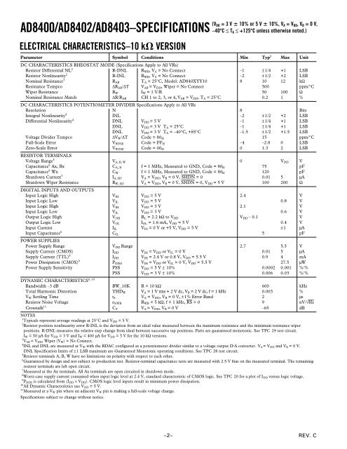
<strong>AD8400</strong>/<strong>AD8402</strong>/<strong>AD8403</strong>–<strong>SP</strong>ECIFICATIONS (V DD = 3 V 10% or 5 V 10%, V A = V DD , V B = 0 V,<br />
–40C ≤ T A ≤ +125C unless otherwise noted.)<br />
ELECTRICAL CHARACTERISTICS–10 k VERSION<br />
Parameter Symbol Conditions Min Typ 1 Max Unit<br />
DC CHARACTERISTICS RHEOSTAT MODE (Specifications Apply to All VRs)<br />
Resistor Differential NL 2 R-DNL R WB , V A = No Connect –1 ± 1/4 +1 LSB<br />
Resistor Nonlinearity 2 R-INL R WB , V A = No Connect –2 ± 1/2 +2 LSB<br />
Nominal Resistance 3 R AB T A = 25°C, Model: AD840XYY10 8 10 12 kΩ<br />
Resistance Tempco ∆R AB /∆T V AB = V DD , Wiper = No Connect 500 ppm/°C<br />
Wiper Resistance R W I W = 1 V/R 50 100 Ω<br />
Nominal Resistance Match ∆R/R AB CH 1 to 2, 3, or 4, V AB = V DD , T A = 25°C 0.2 1 %<br />
DC CHARACTERISTICS POTENTIOMETER DIVIDER Specifications Apply to All VRs<br />
Resolution N 8 Bits<br />
Integral Nonlinearity 4 INL –2 ± 1/2 +2 LSB<br />
Differential Nonlinearity 4 DNL V DD = 5 V –1 ± 1/4 +1 LSB<br />
DNL V DD = 3 V T A = 25°C –1 ± 1/4 +1 LSB<br />
DNL V DD = 3 V T A = –40°C, +85°C –1.5 ± 1/2 +1.5 LSB<br />
Voltage Divider Tempco ∆V W /∆T Code = 80 H 15 ppm/°C<br />
Full-Scale Error V WFSE Code = FF H –4 –2.8 0 LSB<br />
Zero-Scale Error V WZSE Code = 00 H 0 1.3 2 LSB<br />
RESISTOR TERMINALS<br />
Voltage Range 5 V A, B, W 0 V DD V<br />
Capacitance 6 Ax, Bx C A, B f = 1 MHz, Measured to GND, Code = 80 H 75 pF<br />
Capacitance 6 Wx C W f = 1 MHz, Measured to GND, Code = 80 H 120 pF<br />
Shutdown Current 7 I A_SD V A = V DD , V B = 0 V, SHDN = 0 0.01 5 µA<br />
Shutdown Wiper Resistance R W_SD V A = V DD , V B = 0 V, SHDN = 0, V DD = 5 V 100 200 Ω<br />
DIGITAL INPUTS AND OUTPUTS<br />
Input Logic High V IH V DD = 5 V 2.4 V<br />
Input Logic Low V IL V DD = 5 V 0.8 V<br />
Input Logic High V IH V DD = 3 V 2.1 V<br />
Input Logic Low V IL V DD = 3 V 0.6 V<br />
Output Logic High V OH R L = 2.2 kΩ to V DD V DD – 0.1 V<br />
Output Logic Low V OL I OL = 1.6 mA, V DD = 5 V 0.4 V<br />
Input Current I IL V IN = 0 V or +5 V, V DD = 5 V ± 1 µA<br />
Input Capacitance 6 C IL 5 pF<br />
POWER SUPPLIES<br />
Power Supply Range V DD Range 2.7 5.5 V<br />
Supply Current (CMOS) I DD V IH = V DD or V IL = 0 V 0.01 5 µA<br />
Supply Current (TTL) 8 I DD V IH = 2.4 V or 0.8 V, V DD = 5.5 V 0.9 4 mA<br />
Power Dissipation (CMOS) 9 P DISS V IH = V DD or V IL = 0 V, V DD = 5.5 V 27.5 µW<br />
Power Supply Sensitivity PSS V DD = 5 V ± 10% 0.0002 0.001 %/%<br />
PSS V DD = 3 V ± 10% 0.006 0.03 %/%<br />
6, 10<br />
DYNAMIC CHARACTERISTICS<br />
Bandwidth –3 dB BW_10K R = 10 kΩ 600 kHz<br />
Total Harmonic Distortion THD W V A = 1 V rms + 2 V dc, V B = 2 V dc, f = 1 kHz 0.003 %<br />
V W Settling Time t S V A = V DD , V B = 0 V, ±1% Error Band 2 µs<br />
Resistor Noise Voltage e NWB R WB = 5 kΩ, f = 1 kHz, RS = 0 9 nV/√Hz<br />
Crosstalk 11 C T V A = V DD , V B = 0 V –65 dB<br />
NOTES<br />
11 Typicals represent average readings at 25°C and V DD = 5 V.<br />
12 Resistor position nonlinearity error R-INL is the deviation from an ideal value measured between the maximum resistance and the minimum resistance wiper<br />
1 positions. R-DNL measures the relative step change from ideal between successive tap positions. Parts are guaranteed monotonic. See TPC 29 test circuit.<br />
1 I W = 50 µA for V DD = 3 V and I W = 400 µA for V DD = 5 V for the 10 kΩ versions.<br />
13 V AB = V DD , Wiper (V W ) = No Connect.<br />
14 INL and DNL are measured at V W with the RDAC configured as a potentiometer divider similar to a voltage output D/A converter. V A = V DD and V B = 0 V.<br />
1 DNL Specification limits of ±1 LSB maximum are Guaranteed Monotonic operating conditions. See TPC 28 test circuit.<br />
15 Resistor terminals A, B, W have no limitations on polarity with respect to each other.<br />
16 Guaranteed by design and not subject to production test. Resistor-terminal capacitance tests are measured with 2.5 V bias on the measured terminal. The remaining<br />
1 resistor terminals are left open circuit.<br />
17 Measured at the Ax terminals. All Ax terminals are open circuited in shutdown mode.<br />
18 Worst-case supply current consumed when input logic level at 2.4 V, standard characteristic of CMOS logic. See TPC 20 for a plot of I DD versus logic voltage.<br />
19 P DISS is calculated from (I DD × V DD ). CMOS logic level inputs result in minimum power dissipation.<br />
10 All Dynamic Characteristics use V DD = 5 V.<br />
11 Measured at a V W pin where an adjacent V W pin is making a full-scale voltage change.<br />
Specifications subject to change without notice.<br />
–2–<br />
REV. C