AD8400/AD8402/AD8403 - SP-Elektroniikka
AD8400/AD8402/AD8403 - SP-Elektroniikka
AD8400/AD8402/AD8403 - SP-Elektroniikka

You also want an ePaper? Increase the reach of your titles
YUMPU automatically turns print PDFs into web optimized ePapers that Google loves.
a<br />
FEATURES<br />
256-Position<br />
Replaces 1, 2, or 4 Potentiometers<br />
1 k, 10 k, 50 k, 100 k<br />
Power Shutdown—Less than 5 A<br />
3-Wire <strong>SP</strong>I-Compatible Serial Data Input<br />
10 MHz Update Data Loading Rate<br />
2.7 V to 5.5 V Single-Supply Operation<br />
Midscale Preset<br />
APPLICATIONS<br />
Mechanical Potentiometer Replacement<br />
Programmable Filters, Delays, Time Constants<br />
Volume Control, Panning<br />
Line Impedance Matching<br />
Power Supply Adjustment<br />
V DD<br />
DGND<br />
SDI<br />
CLK<br />
CS<br />
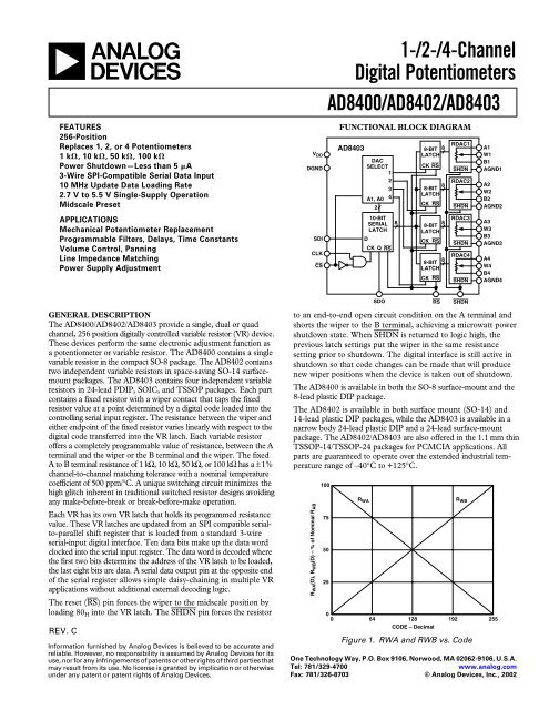
1-/2-/4-Channel<br />
Digital Potentiometers<br />
<strong>AD8400</strong>/<strong>AD8402</strong>/<strong>AD8403</strong><br />
FUNCTIONAL BLOCK DIAGRAM<br />
<strong>AD8403</strong><br />
DAC<br />
SELECT<br />
1<br />
2<br />
D<br />
A1, A0<br />
2<br />
10-BIT<br />
SERIAL<br />
LATCH<br />
3<br />
4<br />
CK Q RS<br />
8<br />
8-BIT 8<br />
LATCH<br />
CK RS<br />
8<br />
8-BIT<br />
LATCH<br />
CK RS<br />
8<br />
8-BIT<br />
LATCH<br />
CK RS<br />
8-BIT<br />
LATCH<br />
CK RS<br />
8<br />
RDAC1<br />
SHDN<br />
RDAC2<br />
SHDN<br />
RDAC3<br />
SHDN<br />
RDAC4<br />
SHDN<br />
A1<br />
W1<br />
B1<br />
AGND1<br />
A2<br />
W2<br />
B2<br />
AGND2<br />
A3<br />
W3<br />
B3<br />
AGND3<br />
A4<br />
W4<br />
B4<br />
AGND4<br />
GENERAL DESCRIPTION<br />
The <strong>AD8400</strong>/<strong>AD8402</strong>/<strong>AD8403</strong> provide a single, dual or quad<br />
channel, 256 position digitally controlled variable resistor (VR) device.<br />
These devices perform the same electronic adjustment function as<br />
a potentiometer or variable resistor. The <strong>AD8400</strong> contains a single<br />
variable resistor in the compact SO-8 package. The <strong>AD8402</strong> contains<br />
two independent variable resistors in space-saving SO-14 surfacemount<br />
packages. The <strong>AD8403</strong> contains four independent variable<br />
resistors in 24-lead PDIP, SOIC, and TSSOP packages. Each part<br />
contains a fixed resistor with a wiper contact that taps the fixed<br />
resistor value at a point determined by a digital code loaded into the<br />
controlling serial input register. The resistance between the wiper and<br />
either endpoint of the fixed resistor varies linearly with respect to the<br />
digital code transferred into the VR latch. Each variable resistor<br />
offers a completely programmable value of resistance, between the A<br />
terminal and the wiper or the B terminal and the wiper. The fixed<br />
A to B terminal resistance of 1 kΩ, 10 kΩ, 50 kΩ, or 100 kΩ has a ±1%<br />
channel-to-channel matching tolerance with a nominal temperature<br />
coefficient of 500 ppm/°C. A unique switching circuit minimizes the<br />
high glitch inherent in traditional switched resistor designs avoiding<br />
any make-before-break or break-before-make operation.<br />
Each VR has its own VR latch that holds its programmed resistance<br />
value. These VR latches are updated from an <strong>SP</strong>I compatible serialto-parallel<br />
shift register that is loaded from a standard 3-wire<br />
serial-input digital interface. Ten data bits make up the data word<br />
clocked into the serial input register. The data word is decoded where<br />
the first two bits determine the address of the VR latch to be loaded,<br />
the last eight bits are data. A serial data output pin at the opposite end<br />
of the serial register allows simple daisy-chaining in multiple VR<br />
applications without additional external decoding logic.<br />
The reset (RS) pin forces the wiper to the midscale position by<br />
loading 80 H into the VR latch. The SHDN pin forces the resistor<br />
REV. C<br />
Information furnished by Analog Devices is believed to be accurate and<br />
reliable. However, no responsibility is assumed by Analog Devices for its<br />
use, nor for any infringements of patents or other rights of third parties that<br />
may result from its use. No license is granted by implication or otherwise<br />
under any patent or patent rights of Analog Devices.<br />
SDO<br />
SHDN<br />
to an end-to-end open circuit condition on the A terminal and<br />
shorts the wiper to the B terminal, achieving a microwatt power<br />
shutdown state. When SHDN is returned to logic high, the<br />
previous latch settings put the wiper in the same resistance<br />
setting prior to shutdown. The digital interface is still active in<br />
shutdown so that code changes can be made that will produce<br />
new wiper positions when the device is taken out of shutdown.<br />
The <strong>AD8400</strong> is available in both the SO-8 surface-mount and the<br />
8-lead plastic DIP package.<br />
The <strong>AD8402</strong> is available in both surface mount (SO-14) and<br />
14-lead plastic DIP packages, while the <strong>AD8403</strong> is available in a<br />
narrow body 24-lead plastic DIP and a 24-lead surface-mount<br />
package. The <strong>AD8402</strong>/<strong>AD8403</strong> are also offered in the 1.1 mm thin<br />
TSSOP-14/TSSOP-24 packages for PCMCIA applications. All<br />
parts are guaranteed to operate over the extended industrial temperature<br />
range of –40°C to +125°C.<br />
R WA (D), R WB (D) – % of Nominal R AB<br />
100<br />
75<br />
50<br />
25<br />
R WA<br />
0<br />
0 64 128 192 255<br />
CODE – Decimal<br />
One Technology Way, P.O. Box 9106, Norwood, MA 02062-9106, U.S.A.<br />
Tel: 781/329-4700<br />
www.analog.com<br />
Fax: 781/326-8703 © Analog Devices, Inc., 2002<br />
RS<br />
R WB<br />
Figure 1. RWA and RWB vs. Code
<strong>AD8400</strong>/<strong>AD8402</strong>/<strong>AD8403</strong>–<strong>SP</strong>ECIFICATIONS (V DD = 3 V 10% or 5 V 10%, V A = V DD , V B = 0 V,<br />
–40C ≤ T A ≤ +125C unless otherwise noted.)<br />
ELECTRICAL CHARACTERISTICS–10 k VERSION<br />
Parameter Symbol Conditions Min Typ 1 Max Unit<br />
DC CHARACTERISTICS RHEOSTAT MODE (Specifications Apply to All VRs)<br />
Resistor Differential NL 2 R-DNL R WB , V A = No Connect –1 ± 1/4 +1 LSB<br />
Resistor Nonlinearity 2 R-INL R WB , V A = No Connect –2 ± 1/2 +2 LSB<br />
Nominal Resistance 3 R AB T A = 25°C, Model: AD840XYY10 8 10 12 kΩ<br />
Resistance Tempco ∆R AB /∆T V AB = V DD , Wiper = No Connect 500 ppm/°C<br />
Wiper Resistance R W I W = 1 V/R 50 100 Ω<br />
Nominal Resistance Match ∆R/R AB CH 1 to 2, 3, or 4, V AB = V DD , T A = 25°C 0.2 1 %<br />
DC CHARACTERISTICS POTENTIOMETER DIVIDER Specifications Apply to All VRs<br />
Resolution N 8 Bits<br />
Integral Nonlinearity 4 INL –2 ± 1/2 +2 LSB<br />
Differential Nonlinearity 4 DNL V DD = 5 V –1 ± 1/4 +1 LSB<br />
DNL V DD = 3 V T A = 25°C –1 ± 1/4 +1 LSB<br />
DNL V DD = 3 V T A = –40°C, +85°C –1.5 ± 1/2 +1.5 LSB<br />
Voltage Divider Tempco ∆V W /∆T Code = 80 H 15 ppm/°C<br />
Full-Scale Error V WFSE Code = FF H –4 –2.8 0 LSB<br />
Zero-Scale Error V WZSE Code = 00 H 0 1.3 2 LSB<br />
RESISTOR TERMINALS<br />
Voltage Range 5 V A, B, W 0 V DD V<br />
Capacitance 6 Ax, Bx C A, B f = 1 MHz, Measured to GND, Code = 80 H 75 pF<br />
Capacitance 6 Wx C W f = 1 MHz, Measured to GND, Code = 80 H 120 pF<br />
Shutdown Current 7 I A_SD V A = V DD , V B = 0 V, SHDN = 0 0.01 5 µA<br />
Shutdown Wiper Resistance R W_SD V A = V DD , V B = 0 V, SHDN = 0, V DD = 5 V 100 200 Ω<br />
DIGITAL INPUTS AND OUTPUTS<br />
Input Logic High V IH V DD = 5 V 2.4 V<br />
Input Logic Low V IL V DD = 5 V 0.8 V<br />
Input Logic High V IH V DD = 3 V 2.1 V<br />
Input Logic Low V IL V DD = 3 V 0.6 V<br />
Output Logic High V OH R L = 2.2 kΩ to V DD V DD – 0.1 V<br />
Output Logic Low V OL I OL = 1.6 mA, V DD = 5 V 0.4 V<br />
Input Current I IL V IN = 0 V or +5 V, V DD = 5 V ± 1 µA<br />
Input Capacitance 6 C IL 5 pF<br />
POWER SUPPLIES<br />
Power Supply Range V DD Range 2.7 5.5 V<br />
Supply Current (CMOS) I DD V IH = V DD or V IL = 0 V 0.01 5 µA<br />
Supply Current (TTL) 8 I DD V IH = 2.4 V or 0.8 V, V DD = 5.5 V 0.9 4 mA<br />
Power Dissipation (CMOS) 9 P DISS V IH = V DD or V IL = 0 V, V DD = 5.5 V 27.5 µW<br />
Power Supply Sensitivity PSS V DD = 5 V ± 10% 0.0002 0.001 %/%<br />
PSS V DD = 3 V ± 10% 0.006 0.03 %/%<br />
6, 10<br />
DYNAMIC CHARACTERISTICS<br />
Bandwidth –3 dB BW_10K R = 10 kΩ 600 kHz<br />
Total Harmonic Distortion THD W V A = 1 V rms + 2 V dc, V B = 2 V dc, f = 1 kHz 0.003 %<br />
V W Settling Time t S V A = V DD , V B = 0 V, ±1% Error Band 2 µs<br />
Resistor Noise Voltage e NWB R WB = 5 kΩ, f = 1 kHz, RS = 0 9 nV/√Hz<br />
Crosstalk 11 C T V A = V DD , V B = 0 V –65 dB<br />
NOTES<br />
11 Typicals represent average readings at 25°C and V DD = 5 V.<br />
12 Resistor position nonlinearity error R-INL is the deviation from an ideal value measured between the maximum resistance and the minimum resistance wiper<br />
1 positions. R-DNL measures the relative step change from ideal between successive tap positions. Parts are guaranteed monotonic. See TPC 29 test circuit.<br />
1 I W = 50 µA for V DD = 3 V and I W = 400 µA for V DD = 5 V for the 10 kΩ versions.<br />
13 V AB = V DD , Wiper (V W ) = No Connect.<br />
14 INL and DNL are measured at V W with the RDAC configured as a potentiometer divider similar to a voltage output D/A converter. V A = V DD and V B = 0 V.<br />
1 DNL Specification limits of ±1 LSB maximum are Guaranteed Monotonic operating conditions. See TPC 28 test circuit.<br />
15 Resistor terminals A, B, W have no limitations on polarity with respect to each other.<br />
16 Guaranteed by design and not subject to production test. Resistor-terminal capacitance tests are measured with 2.5 V bias on the measured terminal. The remaining<br />
1 resistor terminals are left open circuit.<br />
17 Measured at the Ax terminals. All Ax terminals are open circuited in shutdown mode.<br />
18 Worst-case supply current consumed when input logic level at 2.4 V, standard characteristic of CMOS logic. See TPC 20 for a plot of I DD versus logic voltage.<br />
19 P DISS is calculated from (I DD × V DD ). CMOS logic level inputs result in minimum power dissipation.<br />
10 All Dynamic Characteristics use V DD = 5 V.<br />
11 Measured at a V W pin where an adjacent V W pin is making a full-scale voltage change.<br />
Specifications subject to change without notice.<br />
–2–<br />
REV. C
REV. C –3–<br />
<strong>AD8400</strong>/<strong>AD8402</strong>/<strong>AD8403</strong><br />
<strong>SP</strong>ECIFICATIONS (V DD = 3 V 10% or 5 V 10%, V A = V DD , V B = 0 V, –40C ≤ T A ≤ +125C unless otherwise noted.)<br />
ELECTRICAL CHARACTERISTICS–50 k and 100 k VERSIONS<br />
Parameter Symbol Conditions Min Typ 1 Max Unit<br />
DC CHARACTERISTICS RHEOSTAT MODE (Specifications Apply to All VRs)<br />
Resistor Differential NL 2 R-DNL R WB , V A = No Connect –1 ± 1/4 +1 LSB<br />
Resistor Nonlinearity 2 R-INL R WB , V A = No Connect –2 ± 1/2 +2 LSB<br />
Nominal Resistance 3 R AB T A = 25°C, Model: AD840XYY50 35 50 65 kΩ<br />
R AB T A = 25°C, Model: AD840XYY100 70 100 130 kΩ<br />
Resistance Tempco ∆R AB /∆T V AB = V DD , Wiper = No Connect 500 ppm/°C<br />
Wiper Resistance R W I W = 1 V/R 53 100 Ω<br />
Nominal Resistance Match ∆R/R AB CH 1 to 2, 3, or 4, V AB = V DD , T A = 25°C 0.2 1 %<br />
DC CHARACTERISTICS POTENTIOMETER DIVIDER (Specifications Apply to All VRs)<br />
Resolution N 8 Bits<br />
Integral Nonlinearity 4 INL –4 ± 1 +4 LSB<br />
Differential Nonlinearity 4 DNL V DD = 5 V –1 ± 1/4 +1 LSB<br />
DNL V DD = 3 V T A = 25°C –1 ± 1/4 +1 LSB<br />
DNL V DD = 3 V T A = –40°C, +85°C –1.5 ± 1/2 +1.5 LSB<br />
Voltage Divider Tempco ∆V W /∆T Code = 80 H 15 ppm/°C<br />
Full-Scale Error V WFSE Code = FF H –1 –0.25 0 LSB<br />
Zero-Scale Error V WZSE Code = 00 H 0 +0.1 +1 LSB<br />
RESISTOR TERMINALS<br />
Voltage Range 5 V A, B, W 0 V DD V<br />
Capacitance 6 Ax, Bx C A, B f = 1 MHz, Measured to GND, Code = 80 H 15 pF<br />
Capacitance 6 Wx C W f = 1 MHz, Measured to GND, Code = 80 H 80 pF<br />
Shutdown Current 7 I A_SD V A = V DD , V B = 0 V, SHDN = 0 0.01 5 µA<br />
Shutdown Wiper Resistance R W_SD V A = V DD , V B = 0 V, SHDN = 0, V DD = 5 V 100 200 Ω<br />
DIGITAL INPUTS AND OUTPUTS<br />
Input Logic High V IH V DD = 5 V 2.4 V<br />
Input Logic Low V IL V DD = 5 V 0.8 V<br />
Input Logic High V IH V DD = 3 V 2.1 V<br />
Input Logic Low V IL V DD = 3 V 0.6 V<br />
Output Logic High V OH R L = 2.2 kΩ to V DD V DD – 0.1 V<br />
Output Logic Low V OL I OL = 1.6 mA, V DD = 5 V 0.4 V<br />
Input Current I IL V IN = 0 V or 5 V, V DD = 5 V ± 1 µA<br />
Input Capacitance 6 C IL 5 pF<br />
POWER SUPPLIES<br />
Power Supply Range V DD Range 2.7 5.5 V<br />
Supply Current (CMOS) I DD V IH = V DD or V IL = 0 V 0.01 5 µA<br />
Supply Current (TTL) 8 I DD V IH = 2.4 V or 0.8 V, V DD = 5.5 V 0.9 4 mA<br />
Power Dissipation (CMOS) 9 P DISS V IH = V DD or V IL = 0 V, V DD = 5.5 V 27.5 µW<br />
Power Supply Sensitivity PSS V DD = 5 V ± 10% 0.0002 0.001 %/%<br />
PSS V DD = 3 V ± 10% 0.006 0.03 %/%<br />
6, 10<br />
DYNAMIC CHARACTERISTICS<br />
Bandwidth –3 dB BW_50K R = 50 kΩ 125 kHz<br />
BW_100K R = 100 kΩ 71 kHz<br />
Total Harmonic Distortion THD W V A = 1 V rms + 2 V dc, V B = 2 V dc, f = 1 kHz 0.003 %<br />
V W Settling Time t S _50K V A = V DD , V B = 0 V, ±1% Error Band 9 µs<br />
t S _100K V A = V DD , V B = 0 V, ±1% Error Band 18 µs<br />
Resistor Noise Voltage e NWB _50K R WB = 25 kΩ, f = 1 kHz, RS = 0 20 nV/√Hz<br />
e NWB _100K R WB = 50 kΩ, f = 1 kHz, RS = 0 29 nV/√Hz<br />
Crosstalk 11 C T V A = V DD , V B = 0 V –65 dB<br />
NOTES<br />
11 Typicals represent average readings at 25°C and V DD = 5 V.<br />
12 Resistor position nonlinearity error R-INL is the deviation from an ideal value measured between the maximum resistance and the minimum resistance wiper<br />
1 positions. R-DNL measures the relative step change from ideal between successive tap positions. Parts are guaranteed monotonic. See TPC 29 test circuit.<br />
1 I W = V DD /R for V DD = 3 V or 5 V for the 50 kΩ and 100 kΩ versions.<br />
13 V AB = V DD , Wiper (V W ) = No Connect.<br />
14 INL and DNL are measured at V W with the RDAC configured as a potentiometer divider similar to a voltage output D/A converter. V A = V DD and V B = 0 V.<br />
1 DNL Specification limits of ±1 LSB maximum are Guaranteed Monotonic operating conditions. See TPC 28 test circuit.<br />
15 Resistor terminals A, B, W have no limitations on polarity with respect to each other.<br />
16 Guaranteed by design and not subject to production test. Resistor-terminal capacitance tests are measured with 2.5 V bias on the measured terminal. The remaining<br />
1 resistor terminals are left open circuit.<br />
17 Measured at the Ax terminals. All Ax terminals are open circuited in shutdown mode.<br />
18 Worst-case supply current consumed when input logic level at 2.4 V, standard characteristic of CMOS logic. See TPC 20 for a plot of I DD versus logic voltage.<br />
19 P DISS is calculated from (I DD × V DD ). CMOS logic level inputs result in minimum power dissipation.<br />
10 All Dynamic Characteristics use V DD = 5 V.<br />
11 Measured at a V W pin where an adjacent V W pin is making a full-scale voltage change.<br />
Specifications subject to change without notice.
<strong>AD8400</strong>/<strong>AD8402</strong>/<strong>AD8403</strong>–<strong>SP</strong>ECIFICATIONS (V DD = 3 V 10% or 5 V 10%, V A = V DD , V B = 0 V,<br />
–40C ≤ T A ≤ +125C unless otherwise noted.)<br />
ELECTRICAL CHARACTERISTICS–1 k VERSION<br />
Parameter Symbol Conditions Min Typ 1 Max Unit<br />
DC CHARACTERISTICS RHEOSTAT MODE Specifications Apply to All VRs<br />
Resistor Differential NL 2 R-DNL R WB , V A = No Connect –5 –1 +3 LSB<br />
Resistor Nonlinearity 2 R-INL R WB , V A = No Connect –4 ± 1.5 +4 LSB<br />
Nominal Resistance 3 R AB T A = 25°C, Model: AD840XYY1 0.8 1.2 1.6 kΩ<br />
Resistance Tempco ∆R AB /∆T V AB = V DD , Wiper = No Connect 700 ppm/°C<br />
Wiper Resistance R W I W = 1 V/R AB 53 100 Ω<br />
Nominal Resistance Match ∆R/R AB CH 1 to 2, V AB = V DD , T A = 25°C 0.75 2 %<br />
DC CHARACTERISTICS POTENTIOMETER DIVIDER Specifications Apply to All VRs<br />
Resolution N 8 Bits<br />
Integral Nonlinearity 4 INL –6 ± 2 +6 LSB<br />
Differential Nonlinearity 4 DNL V DD = 5 V –4 –1.5 +2 LSB<br />
DNL V DD = 3 V, T A = 25°C –5 –2 +5 LSB<br />
Voltage Divider Temperature Coefficent ∆V W /∆T Code = 80 H 25 ppm/°C<br />
Full-Scale Error V WFSE Code = FF H –20 –12 0 LSB<br />
Zero-Scale Error V WZSE Code = 00 H 0 6 10 LSB<br />
RESISTOR TERMINALS<br />
Voltage Range 5 V A, B, W 0 V DD V<br />
Capacitance 6 Ax, Bx C A, B f = 1 MHz, Measured to GND, Code = 80 H 75 pF<br />
Capacitance 6 Wx C W f = 1 MHz, Measured to GND, Code = 80 H 120 pF<br />
Shutdown Supply Current 7 I A_SD V A = V DD , V B = 0 V, SHDN = 0 0.01 5 µA<br />
Shutdown Wiper Resistance R W_SD V A = V DD , V B = 0 V, SHDN = 0, V DD = 5 V 50 100 Ω<br />
DIGITAL INPUTS AND OUTPUTS<br />
Input Logic High V IH V DD = 5 V 2.4 V<br />
Input Logic Low V IL V DD = 5 V 0.8 V<br />
Input Logic High V IH V DD = 3 V 2.1 V<br />
Input Logic Low V IL V DD = 3 V 0.6 V<br />
Output Logic High V OH R L = 2.2 kΩ to V DD V DD – 0.1 V<br />
Output Logic Low V OL I OL = 1.6 mA, V DD = 5 V 0.4 V<br />
Input Current I IL V IN = 0 V or 5 V, V DD = 5 V ± 1 µA<br />
Input Capacitance 6 C IL 5 pF<br />
POWER SUPPLIES<br />
Power Supply Range V DD Range 2.7 5.5 V<br />
Supply Current (CMOS) I DD V IH = V DD or V IL = 0 V 0.01 5 µA<br />
Supply Current (TTL) 8 I DD V IH = 2.4 V or 0.8 V, V DD = 5.5 V 0.9 4 mA<br />
Power Dissipation (CMOS) 9 P DISS V IH = V DD or V IL = 0 V, V DD = 5.5 V 27.5 µW<br />
Power Supply Sensitivity PSS ∆V DD = 5 V ± 10% 0.0035 0.008 %/%<br />
PSS ∆V DD = 3 V ± 10% 0.05 0.13 %/%<br />
6, 10<br />
DYNAMIC CHARACTERISTICS<br />
Bandwidth –3 dB BW_1K R = 1 kΩ 5,000 kHz<br />
Total Harmonic Distortion THD W V A = 1 V rms + 2 V dc, V B = 2 V dc, f = 1 kHz 0.015 %<br />
V W Settling Time t S V A = V DD , V B = 0 V, ± 1% Error Band 0.5 µs<br />
Resistor Noise Voltage e NWB R WB = 500 Ω, f = 1 kHz, RS = 0 3 nV/√Hz<br />
Crosstalk 11 C T V A = V DD , V B = 0 V –65 dB<br />
NOTES<br />
11 Typicals represent average readings at 25°C and V DD = 5 V.<br />
12 Resistor position nonlinearity error R-INL is the deviation from an ideal value measured between the maximum resistance and the minimum resistance wiper<br />
1 positions. R-DNL measures the relative step change from ideal between successive tap positions. See TPC 29 test circuit.<br />
1 I W = 500 µA for V DD = 3 V and I W = 2.5 mA for V DD = 5 V for 1 kΩ version.<br />
13 V AB = V DD , Wiper (V W ) = No Connect.<br />
14 INL and DNL are measured at V W with the RDAC configured as a potentiometer divider similar to a voltage output D/A converter. V A = V DD and V B = 0 V.<br />
DNL Specification limits of ±1 LSB maximum are Guaranteed Monotonic operating conditions. See TPC 28 test circuit.<br />
15 Resistor terminals A, B, W have no limitations on polarity with respect to each other.<br />
16 Guaranteed by design and not subject to production test. Resistor-terminal capacitance tests are measured with 2.5 V bias on the measured terminal. The remaining<br />
resistor terminals are left open circuit.<br />
17 Measured at the Ax terminals. All Ax terminals are open circuited in shutdown mode.<br />
18 Worst-case supply current consumed when input logic level at 2.4 V, standard characteristic of CMOS logic. See TPC 20 for a plot of I DD versus logic voltage.<br />
19 P DISS is calculated from (I DD × V DD ). CMOS logic level inputs result in minimum power dissipation.<br />
10 All Dynamic Characteristics use V DD = 5 V.<br />
11 Measured at a V W pin where an adjacent V W pin is making a full-scale voltage change.<br />
Specifications subject to change without notice.<br />
–4–<br />
REV. C
<strong>AD8400</strong>/<strong>AD8402</strong>/<strong>AD8403</strong><br />
<strong>SP</strong>ECIFICATIONS (V DD = 3 V 10% or 5 V 10%, V A = V DD , V B = 0 V, –40C ≤ T A ≤ +125C unless otherwise noted.)<br />
ELECTRICAL CHARACTERISTICS–ALL VERSIONS<br />
Parameter Symbol Conditions Min Typ 1 Max Unit<br />
SWITCHING CHARACTERISTICS 2, 3<br />
Input Clock Pulsewidth t CH , t CL Clock Level High or Low 10 ns<br />
Data Setup Time t DS 5 ns<br />
Data Hold Time t DH 5 ns<br />
CLK to SDO Propagation Delay 4 t PD R L = 1 kΩ to 5 V, C L ≤ 20 pF 1 25 ns<br />
CS Setup Time t CSS 10 ns<br />
CS High Pulsewidth t CSW 10 ns<br />
Reset Pulsewidth t RS 50 ns<br />
CLK Fall to CS Rise Hold Time t CSH 0 ns<br />
CS Rise to Clock Rise Setup t CS1 10 ns<br />
NOTES<br />
1 Typicals represent average readings at 25°C and V DD = 5 V.<br />
2 Guaranteed by design and not subject to production test. Resistor-terminal capacitance tests are measured with 2.5 V bias on the measured terminal. The remaining<br />
resistor terminals are left open circuit.<br />
3 See timing diagram for location of measured values. All input control voltages are specified with t R = t F = 1 ns (10% to 90% of V DD ) and timed from a voltage level<br />
of 1.6 V. Switching characteristics are measured using V DD = 3 V or 5 V. To avoid false clocking, a minimum input logic slew rate of 1 V/µs should be maintained.<br />
4 Propagation Delay depends on value of V DD , R L , and C L —see Applications section.<br />
Specifications subject to change without notice.<br />
1<br />
SDI<br />
0<br />
1<br />
CLK<br />
0<br />
1<br />
CS<br />
0<br />
V DD<br />
V OUT<br />
0V<br />
A1 A0 D7 D6 D5 D4 D3 D2 D1 D0<br />
DAC REGISTER LOAD<br />
SDI<br />
(DATA IN)<br />
1<br />
0<br />
1<br />
SDO<br />
(DATA OUT)<br />
0<br />
1<br />
CLK<br />
0<br />
1<br />
CS<br />
0<br />
V DD<br />
V OUT<br />
0V<br />
Ax OR Dx<br />
A'x OR D'x<br />
t PD_MIN<br />
t CH<br />
t CSS<br />
Ax OR Dx<br />
t DS t DH<br />
A'x OR D'x<br />
t CL<br />
t PD_MAX<br />
tCS1<br />
t CSH<br />
t CSW<br />
t S<br />
1% ERROR BAND<br />
1 %<br />
Figure 2a. Timing Diagram<br />
Figure 2b. Detail Timing Diagram<br />
RS<br />
1<br />
0<br />
t RS<br />
t S<br />
V DD<br />
V OUT<br />
V DD /2 1% ERROR BAND<br />
1%<br />
Figure 2c. Reset Timing Diagram<br />
REV. C –5–
<strong>AD8400</strong>/<strong>AD8402</strong>/<strong>AD8403</strong><br />
ABSOLUTE MAXIMUM RATINGS*<br />
(T A = 25°C, unless otherwise noted.)<br />
V DD to GND . . . . . . . . . . . . . . . . . . . . . . . . . . . . –0.3 V, +8 V<br />
V A , V B , V W to GND . . . . . . . . . . . . . . . . . . . . . . . . . . 0 V, V DD<br />
A X – B X , A X – W X , B X – W X . . . . . . . . . . . . . . . . . . . . . ± 20 mA<br />
Digital Input and Output Voltage to GND . . . . . . . . 0 V, 7 V<br />
Operating Temperature Range . . . . . . . . . . –40°C to +125°C<br />
Maximum Junction Temperature (T J max) . . . . . . . . . . 150°C<br />
Storage Temperature . . . . . . . . . . . . . . . . . . –65°C to +150°C<br />
Lead Temperature (Soldering, 10 sec) . . . . . . . . . . . . . 300°C<br />
Package Power Dissipation . . . . . . . . . . . . . (T J max – T A )/θ JA<br />
Thermal Resistance (θ JA )<br />
P-DIP (N-8) . . . . . . . . . . . . . . . . . . . . . . . . . . . . 103°C/W<br />
SOIC (SO-8) . . . . . . . . . . . . . . . . . . . . . . . . . . . . 158°C/W<br />
P-DIP (N-14) . . . . . . . . . . . . . . . . . . . . . . . . . . . . 83°C/W<br />
P-DIP (N-24) . . . . . . . . . . . . . . . . . . . . . . . . . . . . 63°C/W<br />
SOIC (SO-14) . . . . . . . . . . . . . . . . . . . . . . . . . . . 120°C/W<br />
SOIC (SOL-24) . . . . . . . . . . . . . . . . . . . . . . . . . . . 70°C/W<br />
TSSOP-14 (RU-14) . . . . . . . . . . . . . . . . . . . . . . . 180°C/W<br />
TSSOP-24 (RU-24) . . . . . . . . . . . . . . . . . . . . . . . 143°C/W<br />
*Stresses above those listed under Absolute Maximum Ratings may cause permanent<br />
damage to the device. This is a stress rating only; functional operation of the<br />
device at these or any other conditions above those listed in the operational<br />
sections of this specification is not implied. Exposure to absolute maximum rating<br />
conditions for extended periods may affect device reliability.<br />
Table I. Serial Data Word Format<br />
ADDR<br />
DATA<br />
B9 B8 B7 B6 B5 B4 B3 B2 B1 B0<br />
A1 A0 D7 D6 D5 D4 D3 D2 D1 D0<br />
MSB LSB MSB LSB<br />
2 9 2 8 2 7 2 0<br />
CAUTION<br />
ESD (electrostatic discharge) sensitive device. Electrostatic charges as high as 4000 V readily<br />
accumulate on the human body and test equipment and can discharge without detection. Although<br />
the <strong>AD8400</strong>/<strong>AD8402</strong>/<strong>AD8403</strong> features proprietary ESD protection circuitry, permanent damage<br />
may occur on devices subjected to high-energy electrostatic discharges. Therefore, proper ESD<br />
precautions are recommended to avoid performance degradation or loss of functionality.<br />
WARNING!<br />
ESD SENSITIVE DEVICE<br />
–6–<br />
REV. C
<strong>AD8400</strong>/<strong>AD8402</strong>/<strong>AD8403</strong><br />
Number of<br />
Number of End-to-End Temperature Package Package Devices per Branding<br />
Model Channels R AB (k) Range (C) Description Option* Container Information<br />
<strong>AD8400</strong>AN10 1 10 –40 to +125 PDIP-8 N-8 50 <strong>AD8400</strong>A10<br />
<strong>AD8400</strong>AR10 1 10 –40 to +125 SO-8 SO-8 98 <strong>AD8400</strong>A10<br />
<strong>AD8402</strong>AN10 2 10 –40 to +125 PDIP-14 N-14 25 <strong>AD8402</strong>A10<br />
<strong>AD8402</strong>AR10 2 10 –40 to +125 SO-14 SO-14 56 <strong>AD8402</strong>A10<br />
<strong>AD8402</strong>ARU10 2 10 –40 to +125 TSSOP-14 RU-14 96 8402A10<br />
<strong>AD8402</strong>ARU10-REEL 2 10 –40 to +125 TSSOP-14 RU-14 2,500 8402A10<br />
<strong>AD8403</strong>AN10 4 10 –40 to +125 PDIP-24 N-24 15 <strong>AD8403</strong>A10<br />
<strong>AD8403</strong>AR10 4 10 –40 to +125 SOIC-24 SOL-24 31 <strong>AD8403</strong>A10<br />
<strong>AD8403</strong>ARU10 4 10 –40 to +125 TSSOP-24 RU-24 63 8403A10<br />
<strong>AD8403</strong>ARU10-REEL 4 10 –40 to +125 TSSOP-24 RU-24 2,500 8403A10<br />
<strong>AD8400</strong>AN50 1 50 –40 to +125 PDIP-8 N-8 50 <strong>AD8400</strong>A50<br />
<strong>AD8400</strong>AR50 1 50 –40 to +125 SO-8 SO-8 98 <strong>AD8400</strong>A50<br />
<strong>AD8402</strong>AN50 2 50 –40 to +125 PDIP-14 N-14 25 <strong>AD8402</strong>A50<br />
<strong>AD8402</strong>AR50 2 50 –40 to +125 SO-14 SO-14 56 <strong>AD8402</strong>A50<br />
<strong>AD8402</strong>ARU50 2 50 –40 to +125 TSSOP-14 RU-14 96 8402A50<br />
<strong>AD8402</strong>ARU50-REEL 2 50 –40 to +125 TSSOP-14 RU-14 2,500 8402A50<br />
<strong>AD8403</strong>AN50 4 50 –40 to +125 PDIP-24 N-24 15 <strong>AD8403</strong>A50<br />
<strong>AD8403</strong>AR50 4 50 –40 to +125 SOIC-24 SOL-24 31 <strong>AD8403</strong>A50<br />
<strong>AD8403</strong>ARU50 4 50 –40 to +125 TSSOP-24 RU-24 63 8403A50<br />
<strong>AD8403</strong>ARU50-REEL 4 50 –40 to +125 TSSOP-24 RU-24 2,500 8403A50<br />
<strong>AD8400</strong>AN100 1 100 –40 to +125 PDIP-8 N-8 50 <strong>AD8400</strong>A100<br />
<strong>AD8400</strong>AR100 1 100 –40 to +125 SO-8 SO-8 98 <strong>AD8400</strong>AC<br />
<strong>AD8402</strong>AN100 2 100 –40 to +125 PDIP-14 N-14 25 <strong>AD8402</strong>A100<br />
<strong>AD8402</strong>AR100 2 100 –40 to +125 SO-14 SO-14 56 <strong>AD8402</strong>AC<br />
<strong>AD8402</strong>ARU100 2 100 –40 to +125 TSSOP-14 RU-14 96 8402A-C<br />
<strong>AD8402</strong>ARU100-REEL 2 100 –40 to +125 TSSOP-14 RU-14 2,500 8402A-C<br />
<strong>AD8403</strong>AN100 4 100 –40 to +125 PDIP-24 N-24 15 <strong>AD8403</strong>A100<br />
<strong>AD8403</strong>AR100 4 100 –40 to +125 SOIC-24 SOL-24 31 <strong>AD8403</strong>A100<br />
<strong>AD8403</strong>ARU100 4 100 –40 to +125 TSSOP-24 RU-24 63 8403A100<br />
<strong>AD8403</strong>ARU100-REEL 4 100 –40 to +125 TSSOP-24 RU-24 2,500 8403A100<br />
<strong>AD8400</strong>AN1 1 1 –40 to +125 PDIP-8 N-8 50 <strong>AD8400</strong>A1<br />
<strong>AD8400</strong>AR1 1 1 –40 to +125 SO-8 SO-8 98 <strong>AD8400</strong>A1<br />
<strong>AD8402</strong>AN1 2 1 –40 to +125 PDIP-14 N-14 25 <strong>AD8402</strong>A1<br />
<strong>AD8402</strong>AR1 2 1 –40 to +125 SO-14 SO-14 56 <strong>AD8402</strong>A1<br />
<strong>AD8402</strong>ARU1 2 1 –40 to +125 TSSOP-14 RU-14 96 8402A1<br />
<strong>AD8402</strong>ARU1-REEL 2 1 –40 to +125 TSSOP-14 RU-14 2,500 8402A1<br />
<strong>AD8403</strong>AN1 4 1 –40 to +125 PDIP-24 N-24 15 <strong>AD8403</strong>A1<br />
<strong>AD8403</strong>AR1 4 1 –40 to +125 SOIC-24 SOL-24 31 <strong>AD8403</strong>A1<br />
<strong>AD8403</strong>ARU1 4 1 –40 to +125 TSSOP-24 RU-24 63 8403A1<br />
<strong>AD8403</strong>ARU1-REEL 4 1 –40 to +125 TSSOP-24 RU-24 2,500 8403A1<br />
NOTES<br />
*N = Plastic DIP; SO = Small Outline; RU = Thin Shrink SO<br />
The <strong>AD8400</strong>, <strong>AD8402</strong>, and <strong>AD8403</strong> contain 720 transistors.<br />
ORDERING GUIDE<br />
REV. C<br />
–7–
<strong>AD8400</strong>/<strong>AD8402</strong>/<strong>AD8403</strong><br />
PIN CONFIGURATIONS<br />
<strong>AD8400</strong> PIN FUNCTION DESCRIPTIONS<br />
B1<br />
GND<br />
CS<br />
SDI<br />
AGND<br />
B2<br />
A2<br />
W2<br />
DGND<br />
SHDN<br />
CS<br />
1<br />
2<br />
3<br />
4<br />
<strong>AD8400</strong><br />
TOP VIEW<br />
(Not to Scale)<br />
8 A1<br />
7 W1<br />
6 V DD<br />
5 CLK<br />
1<br />
2<br />
3<br />
<strong>AD8402</strong><br />
14<br />
13<br />
12<br />
B1<br />
A1<br />
W1<br />
4 TOP VIEW 11 V DD<br />
5<br />
(Not to Scale)<br />
10 RS<br />
6<br />
7<br />
9<br />
8<br />
CLK<br />
SDI<br />
Pin Name Description<br />
1 B1 Terminal B RDAC<br />
2 GND Ground<br />
3 CS Chip Select Input, Active Low. When CS<br />
returns high, data in the serial input register<br />
is loaded into the DAC register.<br />
4 SDI Serial Data Input<br />
5 CLK Serial Clock Input, Positive Edge Triggered.<br />
6 V DD Positive power supply, specified for operation<br />
at both 3 V and 5 V.<br />
7 W1 Wiper RDAC, Addr = 00 2<br />
8 A1 Terminal A RDAC<br />
AGND2 1<br />
24 B1<br />
B2<br />
A2<br />
W2<br />
AGND4<br />
2<br />
3<br />
4<br />
5<br />
<strong>AD8403</strong><br />
23 A1<br />
22 W1<br />
21 AGND1<br />
20 B3<br />
B4 6 TOP VIEW 19 A3<br />
A4 7<br />
(Not to Scale)<br />
18 W3<br />
W4 8<br />
17 AGND3<br />
DGND 9<br />
16 V DD<br />
SHDN 10<br />
15 RS<br />
CS 11<br />
SDI 12<br />
14 CLK<br />
13 SDO<br />
<strong>AD8402</strong> PIN FUNCTION DESCRIPTIONS<br />
Pin Name Description<br />
1 AGND Analog Ground*<br />
2 B2 Terminal B RDAC #2<br />
3 A2 Terminal A RDAC #2<br />
4 W2 Wiper RDAC #2, Addr = 01 2 .<br />
5 DGND Digital Ground*<br />
6 SHDN Terminal A Open Circuit. Shutdown controls<br />
Variable Resistors #1 and #2.<br />
7 CS Chip Select Input, Active Low. When CS<br />
returns high, data in the serial input register is<br />
decoded based on the address bits and loaded<br />
into the target DAC register.<br />
8 SDI Serial Data Input<br />
9 CLK Serial Clock Input, Positive Edge Triggered.<br />
10 RS Active low reset to midscale; sets RDAC<br />
registers to 80 H .<br />
11 V DD Positive power supply, specified for operation<br />
at both 3 V and 5 V.<br />
12 W1 Wiper RDAC #1, Addr = 00 2 .<br />
13 A1 Terminal A RDAC #1<br />
14 B1 Terminal B RDAC #1<br />
*All AGNDs must be connected to DGND.<br />
<strong>AD8403</strong> PIN FUNCTION DESCRIPTIONS<br />
Pin Name Description<br />
1 AGND2 Analog Ground #2*<br />
2 B2 Terminal B RDAC #2<br />
3 A2 Terminal A RDAC #2<br />
4 W2 Wiper RDAC #2, Addr = 01 2 .<br />
5 AGND4 Analog Ground #4*<br />
6 B4 Terminal B RDAC #4<br />
7 A4 Terminal A RDAC #4<br />
8 W4 Wiper RDAC #4, Addr = 11 2 .<br />
9 DGND Digital Ground*<br />
10 SHDN Active Low Input. Terminal A open circuit.<br />
Shutdown controls Variable Resistors #1<br />
through #4.<br />
11 CS Chip Select Input, Active Low. When CS<br />
returns high, data in the serial input register<br />
is decoded based on the address bits and<br />
loaded into the target DAC register.<br />
12 SDI Serial Data Input<br />
13 SDO Serial Data Output, Open Drain transistor<br />
requires pull-up resistor.<br />
14 CLK Serial Clock Input, Positive Edge Triggered<br />
15 RS Active Low reset to midscale; sets RDAC<br />
registers to 80 H .<br />
16 V DD Positive power supply, specified for<br />
operation at both 3 V and 5 V.<br />
17 AGND3 Analog Ground #3*<br />
18 W3 Wiper RDAC #3, Addr = 10 2<br />
19 A3 Terminal A RDAC #3<br />
20 B3 Terminal B RDAC #3<br />
21 AGND1 Analog Ground #1*<br />
22 W1 Wiper RDAC #1, Addr = 00 2<br />
23 A1 Terminal A RDAC #1<br />
24 B1 Terminal B RDAC #1<br />
*All AGNDs must be connected to DGND.<br />
–8–<br />
REV. C
Typical Performance Characteristics–<strong>AD8400</strong>/<strong>AD8402</strong>/<strong>AD8403</strong><br />
RESISTANCE – k<br />
10<br />
8<br />
6<br />
4<br />
2<br />
R WB<br />
V DD = 3V OR 5V<br />
R AB = 10k<br />
R WA<br />
V WB VOLTAGE – V<br />
5<br />
4<br />
3<br />
2<br />
1<br />
80 H<br />
FF H<br />
40 H<br />
20 H<br />
05 H<br />
CODE = 10 H<br />
T A = 25C<br />
V DD = 5V<br />
R-INL ERROR – LSB<br />
1<br />
0.5<br />
0<br />
–0.5<br />
T A = –40C<br />
V DD = 5V<br />
T A = +85C<br />
T A = +25C<br />
0<br />
0 32 64 96 128 160 192 224 256<br />
CODE – Decimal<br />
TPC 1. Wiper to End Terminal<br />
Resistance vs. Code<br />
0<br />
0 1 2 3 4 5 6 7<br />
I WB CURRENT – mA<br />
TPC 2. Resistance Linearity vs.<br />
Conduction Current<br />
–1<br />
0 32 64 96 128 160 192 224 256<br />
DIGITAL INPUT CODE – Decimal<br />
TPC 3. Resistance Step Position<br />
Nonlinearity Error vs. Code<br />
FREQUENCY<br />
60<br />
48<br />
36<br />
24<br />
12<br />
SS = 1205 UNITS<br />
V DD = 4.5V<br />
T A = 25C<br />
INL NONLINEARITY ERROR – LSB<br />
1<br />
0.5<br />
0<br />
–0.5<br />
T A = +25C<br />
T A = –40C<br />
T A = +85C<br />
V DD = 5V<br />
FREQUENCY<br />
60<br />
48<br />
36<br />
24<br />
12<br />
SS = 184 UNITS<br />
V DD = 4.5V<br />
T A = 25C<br />
0 40.0 42.5 45.0 47.5 50.0 52.5 55.0 57.5 60.0 62.5 65.0<br />
WIPER RESISTANCE – <br />
–1<br />
0 32 64 96 128 160 192 224 256<br />
DIGITAL INPUT CODE – Decimal<br />
0 35 37 39 41 43 45 47 49 51 53 55<br />
WIPER RESISTANCE – <br />
TPC 4. 10 kΩ Wiper-Contact-<br />
Resistance Histogram<br />
TPC 5. Potentiometer Divider<br />
Nonlinearity Error vs. Code<br />
TPC 6. 50 k Wiper-Contact-<br />
Resistance Histogram<br />
FREQUENCY<br />
60<br />
48<br />
36<br />
24<br />
12<br />
SS = 184 UNITS<br />
V DD = 4.5V<br />
T A = 25C<br />
0 40.0 42.5 45.0 47.5 50.0 52.5 55.0 57.5 60.0 62.5 65.0<br />
WIPER RESISTANCE – <br />
TPC 7. 100 kΩ Wiper-Contact-<br />
Resistance Histogram<br />
NOMINAL RESISTANCE – k<br />
10<br />
8<br />
6<br />
4<br />
2<br />
R AB (END-TO-END)<br />
R WB (WIPER-TO-END)<br />
CODE = 80 H<br />
R AB = 10k<br />
0<br />
–75 –50 –25 0 25 50 75 100 125<br />
TEMPERATURE – C<br />
TPC 8. Nominal Resistance vs.<br />
Temperature<br />
POTENTIOMETER MODE TEMPCO – ppm/C<br />
70<br />
60<br />
50<br />
40<br />
30<br />
20<br />
10<br />
0<br />
V DD = 5V<br />
T A = –40C/+85C<br />
V A = 2.00V<br />
V B = 0V<br />
–10 0 32 64 96 128 160 192 224 256<br />
CODE – Decimal<br />
TPC 9. DV WB /DT Potentiometer<br />
Mode Tempco<br />
REV. C –9–
<strong>AD8400</strong>/<strong>AD8402</strong>/<strong>AD8403</strong><br />
RHEOSTAT MODE TEMPCO – ppm/C<br />
700<br />
600<br />
500<br />
400<br />
300<br />
200<br />
100<br />
0<br />
V DD = 5V<br />
T A = –40C/+85C<br />
V A = NO CONNECT<br />
R WB MEASURED<br />
–100 0 32 64 96 128 160 192 224 256<br />
CODE – Decimal<br />
R W<br />
(20mV/DIV)<br />
CS<br />
(5V/DIV)<br />
TIME 500ns/DIV<br />
GAIN – dB<br />
6<br />
0<br />
–6<br />
–12<br />
–18<br />
–24<br />
–30<br />
–36<br />
CODE = FF<br />
–42<br />
–48<br />
T A = +25C<br />
01<br />
SEE TEST CIRCUIT 7<br />
–54<br />
10 100 1k 10k 100k 1M<br />
FREQUENCY – Hz<br />
80<br />
40<br />
20<br />
10<br />
08<br />
04<br />
02<br />
TPC 10. ∆R WB /∆T Rheostat Mode<br />
Tempco<br />
TPC 11. One Position Step Change at<br />
Half-Scale (Code 7F H to 80 H )<br />
TPC 12. 10 kΩ Gain vs. Frequency<br />
R WB RESISTANCE – %<br />
0.75<br />
0.50<br />
0.25<br />
0<br />
–0.25<br />
–0.50<br />
CODE = 80 H<br />
V DD = 5V<br />
SS = 158 UNITS<br />
AVG + 2 SIGMA<br />
AVG – 2 SIGMA<br />
AVG<br />
OUTPUT<br />
INPUT<br />
THD + NOISE – %<br />
10<br />
1<br />
0.1<br />
0.01<br />
FILTER = 22kHz<br />
V DD = 5V<br />
T A = 25C<br />
SEE TEST CIRCUIT 5<br />
SEE TEST CIRCUIT 6<br />
–0.75<br />
0 100 200 300 400 500 600<br />
HOURS OF OPERATION AT 150C<br />
TPC 13. Long-Term Drift<br />
Accelerated by Burn-In<br />
TIME 500s/DIV<br />
TPC 14. Large Signal Settling Time<br />
0.001<br />
10 100 1k 10k 100k<br />
FREQUENCY – Hz<br />
TPC 15. 50 kΩ Gain vs. Frequency<br />
vs. Code<br />
THD + NOISE – %<br />
10<br />
1<br />
0.1<br />
0.01<br />
FILTER = 22kHz<br />
V DD = 5V<br />
T A = 25C<br />
SEE TEST CIRCUIT 5<br />
SEE TEST CIRCUIT 6<br />
0.001<br />
10 100 1k 10k 100k<br />
FREQUENCY – Hz<br />
TPC 16. Total Harmonic Distortion<br />
Plus Noise vs. Frequency<br />
V OUT<br />
(50mV/DIV)<br />
TIME 200ns/DIV<br />
TPC 17. Digital Feedthrough vs. Time<br />
GAIN – dB<br />
6<br />
0<br />
–6<br />
–12<br />
–18<br />
–24<br />
–30<br />
–36<br />
–42<br />
–48<br />
80 H<br />
40 H<br />
20 H<br />
10 H<br />
08 H<br />
04 H<br />
02 H<br />
01 H<br />
CODE = FF H<br />
–54<br />
1k 10k 100k<br />
1M<br />
FREQUENCY – Hz<br />
TPC 18. 100 kΩ Gain vs. Frequency<br />
vs. Code<br />
–10–<br />
REV. C
NORMALIZED GAIN FLATNESS – 0.1dB/DIV<br />
SEE TEST CIRCUIT 7<br />
CODE = 80 H<br />
V DD = 5V<br />
T A = 25C<br />
R = 50k<br />
R = 100k<br />
R = 10k<br />
10 100 1k 10k 100k 1M<br />
FREQUENCY – Hz<br />
TPC 19. Normalized Gain Flatness vs.<br />
Frequency<br />
IDD – SUPPLY CURRENT – mA<br />
10<br />
1<br />
0.1<br />
T A = 25C<br />
V DD = 3V<br />
V DD = 5V<br />
0.01 0 1 2 3 4 5<br />
DIGITAL INPUT VOLTAGE – V<br />
TPC 20. Supply Current vs.<br />
Digital Input Voltage<br />
<strong>AD8400</strong>/<strong>AD8402</strong>/<strong>AD8403</strong><br />
PSRR – dB<br />
80<br />
60<br />
40<br />
20<br />
V DD = +5V DC 1V p-p AC<br />
T A = 25C<br />
CODE = 80 H<br />
C L = 10pF<br />
V A = 4V, V B = 0V<br />
SEE TEST CIRCUIT 4<br />
0<br />
100 1k 10k 100k 1M<br />
FREQUENCY – Hz<br />
TPC 21. Power Supply Rejection<br />
vs. Frequency<br />
GAIN – dB<br />
12<br />
6<br />
0<br />
–6<br />
–12<br />
–18<br />
–24<br />
f –3dB = 71kHz, R = 100k<br />
f –3dB = 700kHz, R = 10k<br />
f –3dB = 125kHz, R = 50k<br />
–30 V IN = 100mV rms<br />
–36<br />
V DD = 5V<br />
R L = 1M<br />
–42<br />
1k 10k 100k 1M<br />
FREQUENCY – Hz<br />
TPC 22. –3 dB Bandwidths<br />
I DD – SUPPLY CURRENT – µA<br />
1200<br />
A – V DD = 5.5V<br />
CODE = 55 H<br />
1000<br />
B – V DD = 3.3V<br />
CODE = 55 H<br />
800<br />
C – V DD = 5.5V<br />
CODE = FF H<br />
600<br />
D – V DD = 3.3V<br />
CODE = FF H<br />
400<br />
200<br />
T A = 25C<br />
D<br />
0<br />
1k 10k 100k 1M 10M<br />
FREQUENCY – Hz<br />
TPC 23. Supply Current vs.<br />
Clock Frequency<br />
A<br />
B<br />
C<br />
R ON – <br />
160<br />
140<br />
120<br />
100<br />
80<br />
60<br />
40<br />
20<br />
V DD = 2.7V<br />
V DD = 5.5V<br />
SEE TEST CIRCUIT 3<br />
T A = 25C<br />
0<br />
0 1 2 3 4 5 6<br />
V BIAS – V<br />
TPC 24. <strong>AD8403</strong> Incremental Wiper<br />
ON Resistance vs. V DD<br />
100<br />
1<br />
GAIN – dB<br />
PHASE – Degrees<br />
0<br />
–10<br />
–20<br />
0<br />
–45<br />
–90<br />
V DD = 5V<br />
T A = 25C<br />
WIPER SET AT<br />
HALF-SCALE 80 H<br />
I A SHUTDOWN CURRENT – nA<br />
10<br />
V DD = 5V<br />
IDD – SUPPLY CURRENT – A<br />
0.1<br />
0.01<br />
LOGIC INPUT<br />
VOLTAGE = 0, V DD<br />
V DD = 5.5V<br />
V DD = 3.3V<br />
100k<br />
200k 400k 1M 2M 4M 6M 10M<br />
FREQUENCY – Hz<br />
TPC 25. 1 kΩ Gain and Phase<br />
vs. Frequency<br />
1<br />
–55 –35<br />
–15 5 25 45 65 85 105 125<br />
TEMPERATURE – C<br />
TPC 26. Shutdown Current vs.<br />
Temperature<br />
0.001<br />
–55 –35 –15 5 25 45 65 85 105 125<br />
TEMPERATURE – C<br />
TPC 27. Supply Current vs.<br />
Temperature<br />
REV. C<br />
–11–
<strong>AD8400</strong>/<strong>AD8402</strong>/<strong>AD8403</strong><br />
TEST CIRCUITS<br />
A<br />
DUT<br />
B<br />
V+<br />
DUT<br />
A<br />
W<br />
B<br />
V+ = V DD<br />
1LSB = V+/256<br />
V MS<br />
OFFSET<br />
GND<br />
~<br />
W<br />
V IN<br />
2.5V DC<br />
OP279<br />
5V<br />
V OUT<br />
Test Circuit 1. Potentiometer Divider Nonlinearity<br />
Error (INL, DNL)<br />
Test Circuit 5. Inverting Programmable Gain<br />
5V<br />
NO CONNECT<br />
DUT<br />
A<br />
W<br />
B<br />
I W<br />
OFFSET<br />
GND<br />
OP279<br />
V IN<br />
~ W<br />
A B<br />
DUT<br />
2.5V<br />
V OUT<br />
V MS<br />
Test Circuit 2. Resistor Position Nonlinearity<br />
Error (Rheostat Operation; R-INL, R-DNL)<br />
Test Circuit 6. Noninverting Programmable Gain<br />
A<br />
+15V<br />
V IN<br />
2.5V<br />
V+<br />
DUT<br />
A<br />
W<br />
B<br />
I MS<br />
V+ V DD<br />
V I W = 1V/R NOMINAL<br />
W<br />
V W2 – [V W1 + I W (R AW II R BW )]<br />
R W = ––––––––––––––––––––––––––<br />
I W<br />
WHERE V W1 = V MS WHEN<br />
V I W = 0<br />
MS<br />
AND V W2 = V MS WHEN I W = 1/R<br />
OFFSET<br />
GND<br />
~<br />
DUT<br />
B<br />
W<br />
OP42<br />
–15V<br />
V OUT<br />
Test Circuit 3. Wiper Resistance<br />
Test Circuit 7. Gain vs. Frequency<br />
V+<br />
~<br />
V DD<br />
V A<br />
A<br />
W<br />
B<br />
V MS<br />
V+ = V DD 10%<br />
∆V MS<br />
PSRR (dB) = 20LOG ( ––––– )<br />
∆V DD<br />
∆V MS %<br />
PSS (%/%) = –––––––<br />
∆V DD %<br />
DUT<br />
B<br />
W<br />
R SW<br />
= 0.1V<br />
I SW<br />
CODE = ØØ H<br />
+<br />
I SW<br />
0.1V<br />
–<br />
V BIAS<br />
A = NC<br />
Test Circuit 4. Power Supply Sensitivity (PSS, PSRR)<br />
Test Circuit 8. Incremental ON Resistance<br />
–12–<br />
REV. C
<strong>AD8400</strong>/<strong>AD8402</strong>/<strong>AD8403</strong><br />
OPERATION<br />
The <strong>AD8400</strong>/<strong>AD8402</strong>/<strong>AD8403</strong> provide a single, dual, and quad<br />
channel, 256-position digitally controlled variable resistor (VR)<br />
device. Changing the programmed VR settings is accomplished by<br />
clocking in a 10-bit serial data word into the SDI (Serial Data Input)<br />
pin. The format of this data word is two address bits, MSB first,<br />
followed by eight data bits, MSB first. Table I provides the serial<br />
register data word format. The <strong>AD8400</strong>/<strong>AD8402</strong>/<strong>AD8403</strong> has the<br />
following address assignments for the ADDR decode, which<br />
determines the location of VR latch receiving the serial register<br />
data in Bits B7 through B0:<br />
VR# = A1× 2 + A0 + 1 (1)<br />
The single-channel <strong>AD8400</strong> requires A1 = A0 = 0. The dualchannel<br />
<strong>AD8402</strong> requires A1 = 0. VR settings can be changed<br />
one at a time in random sequence. The serial clock running at<br />
10 MHz makes it possible to load all four VRs in under 4 µs<br />
(10 × 4 × 100 ns) for the <strong>AD8403</strong>. The exact timing requirements<br />
are shown in Figures 2a, 2b, and 2c.<br />
The <strong>AD8402</strong>/<strong>AD8403</strong> resets to midscale by asserting the RS<br />
pin, simplifying initial conditions at power up. Both parts have a<br />
power shutdown SHDN pin that places the VR in a zero power<br />
consumption state where terminals Ax are open circuited and the<br />
wiper Wx is connected to Bx resulting in only leakage currents<br />
being consumed in the VR structure. In shutdown mode the VR<br />
latch settings are maintained so that returning to operational mode<br />
from power shutdown, the VR settings return to their previous<br />
resistance values. The digital interface is still active in shutdown,<br />
except that SDO is deactivated. Code changes in the registers can<br />
be made that will produce new wiper positions when the device is<br />
taken out of shutdown.<br />
SHDN<br />
D7<br />
D6<br />
D5<br />
D4<br />
D3<br />
D2<br />
D1<br />
D0<br />
RDAC<br />
LATCH<br />
AND<br />
DECODER<br />
R S<br />
R S<br />
R S<br />
R S<br />
R S = R NOMINAL /256<br />
Figure 3. <strong>AD8402</strong>/<strong>AD8403</strong> Equivalent VR (RDAC) Circuit<br />
Ax<br />
Wx<br />
Bx<br />
PROGRAMMING THE VARIABLE RESISTOR<br />
Rheostat Operation<br />
The nominal resistance of the VR (RDAC) between terminals A and<br />
B is available with values of 1 kΩ, 10 kΩ, 50 kΩ, and 100 kΩ. The<br />
final digits of the part number determine the nominal resistance<br />
value, e.g., 10 kΩ = 10; 100 kΩ = 100. The nominal resistance<br />
(R AB ) of the VR has 256 contact points accessed by the wiper<br />
terminal, plus the B terminal contact. The 8-bit data word in the<br />
RDAC latch is decoded to select one of the 256 possible settings.<br />
The wiper’s first connection starts at the B terminal for data 00 H .<br />
This B terminal connection has a wiper contact resistance of 50 Ω.<br />
The second connection (10 kΩ part) is the first tap point located<br />
at 89 Ω [= R AB (nominal resistance)/256 + R W = 39 Ω + 50 Ω] for<br />
data 01 H . The third connection is the next tap point representing<br />
78 + 50 = 128 Ω for data 02 H . Each LSB data value increase<br />
moves the wiper up the resistor ladder until the last tap point is<br />
reached at 10,011 Ω. The wiper does not directly connect to the<br />
B terminal. See Figure 3 for a simplified diagram of the equivalent<br />
RDAC circuit.<br />
The <strong>AD8400</strong> contains one RDAC, the <strong>AD8402</strong> contains two<br />
independent RDACs, and the <strong>AD8403</strong> contains four independent<br />
RDACs. The general transfer equation that determines the digitally<br />
programmed output resistance between Wx and Bx is:<br />
( )= ( ) × +<br />
R Dx Dx / 256 R R<br />
(2)<br />
WB AB W<br />
where Dx is the data contained in the 8-bit RDAC# latch, and<br />
R AB is the nominal end-to-end resistance.<br />
For example, when V B = 0 V and when the A terminal is open<br />
circuit, the following output resistance values will be set for the<br />
following RDAC latch codes (applies to 10 kΩ potentiometers):<br />
D R WB<br />
(Dec) () Output State<br />
255 10,011 Full Scale<br />
128 5,050 Midscale (RS = 0 Condition)<br />
1 89 1 LSB<br />
0 50 Zero-Scale (Wiper Contact Resistance)<br />
Note in the zero-scale condition a finite wiper resistance of 50 Ω<br />
is present. Care should be taken to limit the current flow between<br />
W and B in this state to a maximum value of 5 mA to avoid<br />
degradation or possible destruction of the internal switch contact.<br />
Like the mechanical potentiometer the RDAC replaces, it is totally<br />
symmetrical. The resistance between the wiper W and terminal<br />
A also produces a digitally controlled complementary resistance<br />
R WA . When these terminals are used, the B terminal can be tied<br />
to the wiper or left floating. Setting the resistance value for R WA<br />
starts at a maximum value of resistance and decreases as the data<br />
loaded in the RDAC latch is increased in value. The general transfer<br />
equation for this operation is:<br />
RWA( DX)= ( 256 − DX) 256 × RAB + RW<br />
(3)<br />
REV. C<br />
–13–
<strong>AD8400</strong>/<strong>AD8402</strong>/<strong>AD8403</strong><br />
where Dx is the data contained in the 8-bit RDAC# latch, and<br />
R AB is the nominal end-to-end resistance. For example, when<br />
V A = 0 V and B terminal is open circuit, the following output<br />
resistance values will be set for the following RDAC latch codes<br />
(applies to 10 kΩ potentiometers):<br />
D<br />
R WA<br />
(Dec) () Output State<br />
255 89 Full-Scale<br />
128 5,050 Midscale (RS = 0 Condition)<br />
1 10,011 1 LSB<br />
0 10,050 Zero-Scale<br />
CS<br />
CLK<br />
SDI<br />
A1<br />
A0<br />
D7<br />
10-BIT<br />
SER<br />
REG<br />
DI D0<br />
8<br />
EN<br />
ADDR<br />
DEC<br />
D7<br />
RDAC<br />
LATCH<br />
D0<br />
#1<br />
<strong>AD8400</strong><br />
GND<br />
V DD<br />
A1<br />
W1<br />
B1<br />
The typical distribution of R AB from channel to channel matches<br />
within ± 1%. However, device-to-device matching is process lotdependent,<br />
having a ± 20% variation. The change in R AB with<br />
temperature has a positive 500 ppm/°C temperature coefficient.<br />
The wiper-to-end-terminal resistance temperature coefficient<br />
has the best performance over the 10% to 100% of adjustment<br />
range where the internal wiper contact switches do not contribute<br />
any significant temperature related errors. The graph in TPC 10<br />
shows the performance of R WB tempco versus code. Using the<br />
trimmer with codes below 32 results in the larger temperature<br />
coefficients plotted.<br />
PROGRAMMING THE POTENTIOMETER DIVIDER<br />
Voltage Output Operation<br />
The digital potentiometer easily generates an output voltage<br />
proportional to the input voltage applied to a given terminal.<br />
For example, connecting A terminal to 5 V and B terminal to<br />
ground produces an output voltage at the wiper starting at zero<br />
volts up to 1 LSB less than 5 V. Each LSB of voltage is equal to<br />
the voltage applied across terminal AB divided by the 256<br />
position resolution of the potentiometer divider. The general<br />
equation defining the output voltage with respect to ground for<br />
any given input voltage applied to terminals AB is:<br />
VW ( DX)= DX 256 × VAB + VB<br />
(4)<br />
Operation of the digital potentiometer in the divider mode results<br />
in more accurate operation over temperature. Here the output<br />
voltage is dependent on the ratio of the internal resistors, not<br />
the absolute value; therefore, the temperature drift improves to<br />
15 ppm/°C.<br />
At the lower wiper position settings, the potentiometer divider<br />
temperature coefficient increases due to the contributions of the<br />
CMOS switch wiper resistance becoming an appreciable portion of<br />
the total resistance from Terminal B to the wiper. See TPC 9 for<br />
a plot of potentiometer tempco performance versus code setting.<br />
CS<br />
CLK<br />
SDO<br />
SDI<br />
CS<br />
CLK<br />
SDI<br />
SHDN<br />
DO<br />
DI<br />
A1<br />
A0<br />
D7<br />
10-BIT<br />
SER<br />
REG<br />
DI D0<br />
DGND<br />
A1<br />
A0<br />
D7<br />
SER<br />
REG<br />
D0<br />
8<br />
8<br />
EN<br />
ADDR<br />
DEC<br />
EN<br />
ADDR<br />
DEC<br />
RS<br />
a.<br />
b.<br />
D7<br />
D0<br />
D7<br />
D0<br />
D7<br />
D0<br />
D7<br />
D0<br />
RDAC<br />
LATCH<br />
#1<br />
R<br />
RDAC<br />
LATCH<br />
#2<br />
R<br />
RDAC<br />
LATCH<br />
#1<br />
R<br />
<strong>AD8402</strong><br />
AGND<br />
<strong>AD8403</strong><br />
RDAC<br />
LATCH<br />
#4<br />
R<br />
V DD<br />
A1<br />
W1<br />
B1<br />
A4<br />
W4<br />
B4<br />
V DD<br />
A1<br />
W1<br />
B1<br />
A4<br />
W4<br />
B4<br />
DIGITAL INTERFACING<br />
The <strong>AD8400</strong>/<strong>AD8402</strong>/<strong>AD8403</strong> contain a standard <strong>SP</strong>I compatible<br />
three-wire serial input control interface. The three inputs<br />
are clock (CLK), CS and serial data input (SDI). The positiveedge<br />
sensitive CLK input requires clean transitions to avoid<br />
clocking incorrect data into the serial input register. For best<br />
results use logic transitions faster than 1 V/µs. Standard logic<br />
families work well. If mechanical switches are used for product<br />
evaluation, they should be debounced by a flip-flop or other<br />
suitable means. The Figure 4 block diagrams show more detail<br />
of the internal digital circuitry. When CS is taken active low, the<br />
clock loads data into the 10-bit serial register on each positive<br />
clock edge (see Table II).<br />
SHDN<br />
DGND<br />
RS<br />
c.<br />
Figure 4. Block Diagrams<br />
AGND<br />
–14–<br />
REV. C
<strong>AD8400</strong>/<strong>AD8402</strong>/<strong>AD8403</strong><br />
Table II. Input Logic Control Truth Table<br />
CLK CS RS SHDN Register Activity<br />
L L H H No SR effect, enables SDO pin.<br />
P L H H Shift one bit in from the SDI pin.<br />
The tenth previously entered bit is<br />
shifted out of the SDO pin.<br />
X P H H Load SR data into RDAC latch<br />
based on A1, A0 decode (Table III).<br />
X H H H No Operation<br />
X X L H Sets all RDAC latches to midscale,<br />
wiper centered, and SDO latch<br />
cleared.<br />
X H P H Latches all RDAC latches to 80 H .<br />
X H H L Open circuits all resistor<br />
A-terminals, connects W to B,<br />
turns off SDO output transistor.<br />
NOTE<br />
P = positive edge, X = don’t care, SR = shift register.<br />
The serial data-output (SDO) pin contains an open drain n-channel<br />
FET. This output requires a pull-up resistor in order to transfer data<br />
to the next package’s SDI pin. The pull-up resistor termination<br />
voltage may be larger than the V DD supply (but less than max<br />
V DD of 8 V) of the <strong>AD8403</strong> SDO output device, e.g., the <strong>AD8403</strong><br />
could operate at V DD = 3.3 V and the pull-up for interface to the<br />
next device could be set at 5 V. This allows for daisy-chaining<br />
several RDACs from a single processor serial data line. The<br />
clock period needs to be increased when using a pull-up resistor<br />
to the SDI pin of the following device in the series. Capacitive<br />
loading at the daisy-chain node SDO–SDI between devices must<br />
be accounted for to successfully transfer data. When daisy chaining<br />
is used, the CS should be kept low until all the bits of every package<br />
are clocked into their respective serial registers ensuring that the<br />
address bits and data bits are in the proper decoding location.<br />
This would require 20 bits of address and data complying to the<br />
word format provided in Table I if two <strong>AD8403</strong> four-channel<br />
RDACs are daisy-chained. Note, only the <strong>AD8403</strong> has a SDO<br />
pin. During shutdown SHDN the SDO output pin is forced to<br />
the off (logic high) state to disable power dissipation in the pull-up<br />
resistor. See Figure 6 for equivalent SDO output circuit schematic.<br />
The data setup and data hold times in the specification table<br />
determine the data valid time requirements. The last 10 bits of<br />
the data word entered into the serial register are held when CS<br />
returns high. At the same time CS goes high it gates the address<br />
decoder, which enables one of the two (<strong>AD8402</strong>) or four (<strong>AD8403</strong>)<br />
positive edge triggered RDAC latches. See Figure 5 detail and<br />
Table III Address Decode Table.<br />
Table III. Address Decode Table<br />
A1 A0 Latch Decoded<br />
0 0 RDAC#1<br />
0 1 RDAC#2<br />
1 0 RDAC#3 <strong>AD8403</strong> Only<br />
1 1 RDAC#4 <strong>AD8403</strong> Only<br />
CS<br />
CLK<br />
SDI<br />
<strong>AD8403</strong><br />
ADDR<br />
DECODE<br />
SERIAL<br />
REGISTER<br />
RDAC 1<br />
RDAC 2<br />
RDAC 4<br />
Figure 5. Equivalent Input Control Logic<br />
The target RDAC latch is loaded with the last eight bits of the<br />
serial data word completing one DAC update. In the case of the<br />
<strong>AD8403</strong> four separate 10-bit data words must be clocked in to<br />
change all four VR settings.<br />
SHDN<br />
CS<br />
SDI<br />
CLK<br />
RS<br />
SERIAL<br />
REGISTER<br />
D<br />
Q<br />
CK RS<br />
SDO<br />
Figure 6. Detail SDO Output Schematic of the <strong>AD8403</strong><br />
All digital pins are protected with a series input resistor and<br />
parallel Zener ESD structure shown in Figure 7a. This structure<br />
applies to digital pins CS, SDI, SDO, RS, SHDN, CLK. The<br />
digital input ESD protection allows for mixed power supply<br />
applications where 5 V CMOS logic can be used to drive an<br />
<strong>AD8400</strong>, <strong>AD8402</strong>, or <strong>AD8403</strong> operating from a 3 V power supply.<br />
The analog pins A, B, and W are protected with a 20 Ω<br />
series resistor and parallel Zener (see Figure 7b).<br />
DIGITAL<br />
PINS<br />
1k<br />
LOGIC<br />
Figure 7a. Equivalent ESD Protection Circuits<br />
A, B, W<br />
20<br />
Figure 7b. Equivalent ESD Protection Circuit<br />
(Analog Pins)<br />
A<br />
C A<br />
C A = 90.4pF (DW / 256) + 30pF<br />
RDAC<br />
10k<br />
W<br />
C W<br />
120pF<br />
C B<br />
B<br />
C B = 90.4pF [1 – (DW / 256)] + 30pF<br />
Figure 8. RDAC Circuit Simulation Model for<br />
RDAC = 10 kΩ<br />
REV. C<br />
–15–
<strong>AD8400</strong>/<strong>AD8402</strong>/<strong>AD8403</strong><br />
The ac characteristics of the RDACs are dominated by the internal<br />
parasitic capacitances and the external capacitive loads. The –3 dB<br />
bandwidth of the <strong>AD8403</strong>AN10 (10 kΩ resistor) measures 600 kHz<br />
at half scale as a potentiometer divider. TPC 22 provides the large<br />
signal BODE plot characteristics of the three available resistor<br />
versions 10 kΩ, 50 kΩ, and 100 kΩ. The gain flatness versus<br />
frequency graph, TPC 25, predicts filter applications performance.<br />
A parasitic simulation model has been developed, and is shown<br />
in Figure 8. Listing I provides a macro model net list for the<br />
10 kΩ RDAC:<br />
Listing I. Macro Model Net List for RDAC<br />
.PARAM DW=255, RDAC=10E3<br />
*<br />
.SUBCKT DPOT (A,W,)<br />
*<br />
CA A 0 {DW/256*90.4E-12+30E-12}<br />
RAW A W {(1-DW/256)*RDAC+50}<br />
CW W 0 120E-12<br />
RBW W B {DW/256*RDAC+50}<br />
CB B 0 {(1-DW/256)*90.4E-12+30E-12}<br />
*<br />
.ENDS DPOT<br />
The total harmonic distortion plus noise (THD+N) is measured<br />
at 0.003% in an inverting op amp circuit using an offset ground<br />
and a rail-to-rail OP279 amplifier, Test Circuit 5. Thermal noise is<br />
primarily Johnson noise, typically 9 nV/√Hz for the 10 kΩ version<br />
at f = 1 kHz. For the 100 kΩ device, thermal noise becomes<br />
29 nV/√Hz. Channel-to-channel crosstalk measures less than<br />
–65 dB at f = 100 kHz. To achieve this isolation, the extra ground<br />
pins provided on the package to segregate the individual RDACs<br />
must be connected to circuit ground. AGND and DGND pins<br />
should be at the same voltage potential. Any unused potentiometers<br />
in a package should be connected to ground. Power<br />
supply rejection is typically –35 dB at 10 kHz. Care is needed to<br />
minimize power supply ripple in high accuracy applications.<br />
APPLICATIONS<br />
The digital potentiometer (RDAC) allows many of the applications<br />
of trimming potentiometers to be replaced by a solid-state solution<br />
offering compact size and freedom from vibration, shock and<br />
open contact problems encountered in hostile environments. A<br />
major advantage of the digital potentiometer is its programmability.<br />
Any settings can be saved for later recall in system memory.<br />
The two major configurations of the RDAC include the<br />
potentiometer divider (basic 3-terminal application) and the<br />
rheostat (2-terminal configuration) connections shown in Test<br />
Circuits 1 and 2 (see page 11).<br />
Certain boundary conditions must be satisfied for proper <strong>AD8400</strong>/<br />
<strong>AD8402</strong>/<strong>AD8403</strong> operation. First, all analog signals must remain<br />
within the 0 to V DD range used to operate the single-supply<br />
<strong>AD8400</strong>/<strong>AD8402</strong>/<strong>AD8403</strong> products. For standard potentiometer<br />
divider applications, the wiper output can be used directly. For<br />
low resistance loads, buffer the wiper with a suitable rail-to-rail<br />
op amp such as the OP291 or the OP279. Second, for ac signals<br />
and bipolar dc adjustment applications, a virtual ground will<br />
generally be needed. Whatever method is used to create the<br />
virtual ground, the result must provide the necessary sink and<br />
source current for all connected loads, including adequate bypass<br />
capacitance. Test Circuit 5 (see page 11) shows one channel of<br />
the <strong>AD8402</strong> connected in an inverting programmable gain<br />
amplifier circuit. The virtual ground is set at 2.5 V, which allows<br />
the circuit output to span a ±2.5 volt range with respect to virtual<br />
ground. The rail-to-rail amplifier capability is necessary for the<br />
widest output swing. As the wiper is adjusted from its midscale<br />
reset position (80 H ) toward the A terminal (code FF H ), the voltage<br />
gain of the circuit is increased in successfully larger increments.<br />
Alternatively, as the wiper is adjusted toward the B terminal<br />
(code 00 H ), the signal becomes attenuated. The plot in Figure 9<br />
shows the wiper settings for a 100:1 range of voltage gain (V/V).<br />
Note the ±10 dB of pseudo-logarithmic gain around 0 dB (1 V/V).<br />
This circuit is mainly useful for gain adjustments in the range of<br />
0.14 V/V to 4 V/V; beyond this range the step sizes become very<br />
large and the resistance of the driving circuit can become a<br />
significant term in the gain equation.<br />
DIGITAL CODE – Decimal<br />
256<br />
224<br />
192<br />
160<br />
128<br />
96<br />
64<br />
32<br />
0<br />
0.1 1.0 10<br />
INVERTING GAIN – V/V<br />
Figure 9. Inverting Programmable Gain Plot<br />
–16–<br />
REV. C
<strong>AD8400</strong>/<strong>AD8402</strong>/<strong>AD8403</strong><br />
ACTIVE FILTER<br />
One of the standard circuits used to generate a low-pass, highpass,<br />
or band-pass filter is the state variable active filter. The<br />
digital potentiometer allows full programmability of the frequency,<br />
gain and Q of the filter outputs. Figure 10 shows the filter circuit<br />
using a 2.5 V virtual ground, which allows a ±2.5 V P input and<br />
output swing. RDAC2 and 3 set the LP, HP, and BP cutoff and<br />
center frequencies, respectively. These variable resistors should<br />
be programmed with the same data (as with ganged potentiometers)<br />
to maintain the best circuit Q. Figure 11 shows the measured<br />
filter response at the band-pass output as a function of the RDAC2<br />
and RDAC3 settings which produce a range of center frequencies<br />
from 2 kHz to 20 kHz. The filter gain response at the band-pass<br />
output is shown in Figure 12. At a center frequency of 2 kHz, the<br />
gain is adjusted over a –20 dB to +20 dB range determined by<br />
RDAC1. Circuit Q is adjusted by RDAC4. For more detailed<br />
reading on the state variable active filter, see Analog Devices’<br />
application note, AN-318.<br />
AMPLITUDE – dB<br />
40<br />
20<br />
0<br />
–20<br />
–40<br />
–60<br />
–0.16 20.0000 k<br />
A<br />
–80 20 100 1k 10k 100k 200k<br />
FREQUENCY – Hz<br />
Figure 11. Programmed Center Frequency Band-Pass<br />
Response<br />
V IN<br />
B RDAC1<br />
A1<br />
RDAC4<br />
B<br />
10k<br />
10k<br />
B<br />
A2<br />
RDAC2<br />
OP279 2<br />
0.01F<br />
A3<br />
B<br />
RDAC3<br />
0.01F<br />
A4<br />
LOW-<br />
PASS<br />
BAND-<br />
PASS<br />
AMPLITUDE – dB<br />
40<br />
20<br />
0<br />
–20<br />
–40<br />
–19.01 2.00000 k<br />
A<br />
HIGH-<br />
PASS<br />
–60<br />
Figure 10. Programmable State Variable Active Filter<br />
–80<br />
20 100 1k 10k<br />
100k 200k<br />
FREQUENCY – Hz<br />
Figure 12. Programmed Amplitude Band-Pass Response<br />
REV. C<br />
–17–
<strong>AD8400</strong>/<strong>AD8402</strong>/<strong>AD8403</strong><br />
OUTLINE DIMENSIONS<br />
Dimensions shown in inches and (mm).<br />
8-Lead Plastic DIP<br />
(N-8)<br />
0.430 (10.92)<br />
0.348 (8.84)<br />
8<br />
5<br />
1 4<br />
0.280 (7.11)<br />
0.240 (6.10)<br />
PIN 1<br />
0.210<br />
(5.33)<br />
MAX<br />
0.160 (4.06)<br />
0.115 (2.93)<br />
0.100 (2.54)<br />
BSC<br />
0.022 (0.558)<br />
0.014 (0.356)<br />
0.070 (1.77)<br />
0.045 (1.15)<br />
0.060 (1.52)<br />
0.015 (0.38)<br />
0.130<br />
(3.30)<br />
MIN<br />
SEATING<br />
PLANE<br />
0.325 (8.25)<br />
0.300 (7.62)<br />
0.195 (4.95)<br />
0.115 (2.93)<br />
0.015 (0.381)<br />
0.008 (0.204)<br />
8-Lead SOIC<br />
(R-8)<br />
0.1968 (5.00)<br />
0.1890 (4.80)<br />
0.1574 (4.00)<br />
0.1497 (3.80)<br />
8 5<br />
1 4<br />
0.2440 (6.20)<br />
0.2284 (5.80)<br />
PIN 1<br />
0.0098 (0.25)<br />
0.0040 (0.10)<br />
0.0688 (1.75)<br />
0.0532 (1.35)<br />
0.0196 (0.50)<br />
0.0099 (0.25) x 45°<br />
SEATING<br />
PLANE<br />
0.0500 0.0192 (0.49)<br />
(1.27) 0.0138 (0.35)<br />
BSC<br />
0.0098 (0.25)<br />
0.0075 (0.19)<br />
8°<br />
0°<br />
0.0500 (1.27)<br />
0.0160 (0.41)<br />
14-Lead Plastic DIP Package<br />
(N-14)<br />
PIN 1<br />
0.210 (5.33)<br />
MAX<br />
0.160 (4.06)<br />
0.115 (2.93)<br />
0.795 (20.19)<br />
0.725 (18.42)<br />
14<br />
8<br />
1 7<br />
0.100 (2.54)<br />
BSC<br />
0.022 (0.558)<br />
0.014 (0.356)<br />
0.070 (1.77)<br />
0.045 (1.15)<br />
0.280 (7.11)<br />
0.240 (6.10)<br />
0.060 (1.52)<br />
0.015 (0.38)<br />
0.130<br />
(3.30)<br />
MIN<br />
SEATING<br />
PLANE<br />
0.325 (8.25)<br />
0.300 (7.62)<br />
0.015 (0.381)<br />
0.008 (0.204)<br />
0.195 (4.95)<br />
0.115 (2.93)<br />
–18–<br />
REV. C
<strong>AD8400</strong>/<strong>AD8402</strong>/<strong>AD8403</strong><br />
14-Lead Narrow Body SOIC Package<br />
(SO-14)<br />
0.3444 (8.75)<br />
0.3367 (8.55)<br />
0.1574 (4.00)<br />
0.1497 (3.80)<br />
14 8<br />
1<br />
7<br />
0.2440 (6.20)<br />
0.2284 (5.80)<br />
PIN 1<br />
0.050 (1.27)<br />
BSC<br />
0.0688 (1.75)<br />
0.0532 (1.35)<br />
0.0196 (0.50)<br />
0.0099 (0.25) 45<br />
0.0098 (0.25)<br />
0.0040 (0.10)<br />
0.0192 (0.49)<br />
0.0138 (0.35)<br />
SEATING<br />
PLANE<br />
0.0099 (0.25)<br />
0.0075 (0.19)<br />
8<br />
0<br />
0.0500 (1.27)<br />
0.0160 (0.41)<br />
14-Lead TSSOP<br />
(RU-14)<br />
0.201 (5.10)<br />
0.193 (4.90)<br />
14 8<br />
1<br />
7<br />
0.177 (4.50)<br />
0.169 (4.30)<br />
0.256 (6.50)<br />
0.246 (6.25)<br />
PIN 1<br />
0.006 (0.15)<br />
0.002 (0.05)<br />
0.0433 (1.10)<br />
MAX<br />
SEATING<br />
PLANE<br />
0.0256<br />
(0.65)<br />
BSC<br />
0.0118 (0.30)<br />
0.0075 (0.19)<br />
8<br />
0<br />
0.0079 (0.20)<br />
0.0035 (0.090)<br />
0.028 (0.70)<br />
0.020 (0.50)<br />
24-Lead Narrow Body Plastic DIP Package<br />
(N-24)<br />
PIN 1<br />
0.210<br />
(5.33)<br />
MAX<br />
0.200 (5.05)<br />
0.125 (3.18)<br />
1.275 (32.30)<br />
1.125 (28.60)<br />
24<br />
13<br />
1 12<br />
0.022 (0.558)<br />
0.014 (0.356)<br />
0.100<br />
(2.54)<br />
BSC<br />
0.070 (1.77)<br />
0.045 (1.15)<br />
0.280 (7.11)<br />
0.240 (6.10)<br />
0.060 (1.52)<br />
0.015 (0.38)<br />
0.150<br />
(3.81)<br />
MIN<br />
SEATING<br />
PLANE<br />
0.325 (8.25)<br />
0.300 (7.62)<br />
0.015 (0.381)<br />
0.008 (0.204)<br />
0.195 (4.95)<br />
0.115 (2.93)<br />
REV. C<br />
–19–
<strong>AD8400</strong>/<strong>AD8402</strong>/<strong>AD8403</strong><br />
OUTLINE DIMENSIONS (continued)<br />
Dimensions shown in inches and (mm).<br />
24-Lead SOIC Package<br />
(SOL-24)<br />
24 13<br />
0.2992 (7.60)<br />
0.2914 (7.40)<br />
1<br />
0.6141 (15.60)<br />
0.5985 (15.20)<br />
12<br />
0.4193 (10.65)<br />
0.3937 (10.00)<br />
C01092–0–2/02(C)<br />
PIN 1<br />
0.1043 (2.65)<br />
0.0926 (2.35)<br />
0.0291 (0.74)<br />
0.0098 (0.25) 45<br />
0.0118 (0.30)<br />
0.0040 (0.10)<br />
0.0500<br />
(1.27)<br />
BSC<br />
0.0192 (0.49)<br />
0.0138 (0.35)<br />
SEATING<br />
PLANE<br />
0.0125 (0.32)<br />
0.0091 (0.23)<br />
8<br />
0<br />
0.0500 (1.27)<br />
0.0157 (0.40)<br />
24-Lead Thin Surface-Mount TSSOP Package<br />
(RU-24)<br />
0.311 (7.90)<br />
0.303 (7.70)<br />
24 13<br />
1<br />
12<br />
0.177 (4.50)<br />
0.169 (4.30)<br />
0.256 (6.50)<br />
0.246 (6.25)<br />
PIN 1<br />
0.006 (0.15)<br />
0.002 (0.05)<br />
0.0433 (1.10)<br />
MAX<br />
SEATING<br />
PLANE<br />
0.0256 (0.65) 0.0118 (0.30)<br />
BSC 0.0075 (0.19)<br />
0.0079 (0.20)<br />
0.0035 (0.090)<br />
8<br />
0<br />
0.028 (0.70)<br />
0.020 (0.50)<br />
Revision History<br />
Location<br />
Page<br />
Data Sheet changed from REV. B to REV. C.<br />
Addition of new Figure 1 . . . . . . . . . . . . . . . . . . . . . . . . . . . . . . . . . . . . . . . . . . . . . . . . . . . . . . . . . . . . . . . . . . . . . . . . . . . . . . . . . . 1<br />
Edits to <strong>SP</strong>ECIFICATIONS . . . . . . . . . . . . . . . . . . . . . . . . . . . . . . . . . . . . . . . . . . . . . . . . . . . . . . . . . . . . . . . . . . . . . . . . . . . . . . . 2<br />
Edits to ABSOLUTE MAXIMUM RATINGS . . . . . . . . . . . . . . . . . . . . . . . . . . . . . . . . . . . . . . . . . . . . . . . . . . . . . . . . . . . . . . . . . 6<br />
Edits to TPCs 1, 8, 12, 16, 20, 24, 35 . . . . . . . . . . . . . . . . . . . . . . . . . . . . . . . . . . . . . . . . . . . . . . . . . . . . . . . . . . . . . . . . . . . . . . . . 9<br />
Edits to PROGRAMMING THE VARIABLE RESISTOR section . . . . . . . . . . . . . . . . . . . . . . . . . . . . . . . . . . . . . . . . . . . . . . . . 13<br />
PRINTED IN U.S.A.<br />
–20–<br />
REV. C