

Atom-chip Bose-Einstein condensation in a portable vacuum cell
Atom-chip Bose-Einstein condensation in a portable vacuum cell
Atom-chip Bose-Einstein condensation in a portable vacuum cell

You also want an ePaper? Increase the reach of your titles
YUMPU automatically turns print PDFs into web optimized ePapers that Google loves.
PHYSICAL REVIEW A 70, 053606 (2004)<br />
<strong>Atom</strong>-<strong>chip</strong> <strong>Bose</strong>-<strong>E<strong>in</strong>ste<strong>in</strong></strong> <strong>condensation</strong> <strong>in</strong> a <strong>portable</strong> <strong>vacuum</strong> <strong>cell</strong><br />
Shengwang Du, 1 Matthew B. Squires, 1 Yutaka Imai, 2 Leslie Czaia, 1 R. A. Saravanan, 3 Victor Bright, 3 Jakob Reichel, 4<br />
T. W. Hänsch, 4 and Dana Z. Anderson 1<br />
1 Department of Physics and JILA, University of Colorado and National Institute of Standards and Technology,<br />
Boulder, Colorado 80309-0440, USA<br />
2 Photonics Research Department, Core Technology Development Group, MSNC, Sony Corporation, Tokyo 141-0001, Japan<br />
3 Department of Mechanical Eng<strong>in</strong>eer<strong>in</strong>g, University of Colorado, Boulder, Colorado 80309-0427, USA<br />
4 Max-Planck-Institut für Quantenoptik and Sektion Physik der Ludwig-Maximilians-Universität, Schell<strong>in</strong>gstrasse 4,<br />
D-80799 München, Germany<br />
(Received 16 April 2004; published 10 November 2004)<br />
A 87 Rb <strong>Bose</strong>-<strong>E<strong>in</strong>ste<strong>in</strong></strong> condensate (BEC) is produced <strong>in</strong> a <strong>portable</strong> atom-<strong>chip</strong> system less than 3030<br />
15 cm, where the ultrahigh <strong>vacuum</strong> is ma<strong>in</strong>ta<strong>in</strong>ed by a small, 8 L/s, ion pump and nonevaporable getter. An<br />
alum<strong>in</strong>um nitride <strong>chip</strong> with lithographically patterned copper is used to seal the <strong>vacuum</strong> system, provide the<br />
electrical feedthroughs, and create the magnetic trap potentials. All cool<strong>in</strong>g and trapp<strong>in</strong>g processes occur<br />
0.6–2.5 mm from ambient laboratory air. A condensate of about 2000 87 Rb atoms <strong>in</strong> F=2,m F =2 is achieved<br />
after 4.21 s of rf forced evaporation. A magneto-optical trap lifetime of 30 s <strong>in</strong>dicates the <strong>vacuum</strong> near the <strong>chip</strong><br />
surface is about 10 −10 torr. This work suggests that a <strong>chip</strong>-based BEC-compatible <strong>vacuum</strong> system can occupy<br />
a volume of less than 0.5 L.<br />
DOI: 10.1103/PhysRevA.70.053606<br />
PACS number(s): 03.75.Be, 32.80.Pj, 39.90.d, 07.30.Kf<br />
From the first <strong>Bose</strong>-<strong>E<strong>in</strong>ste<strong>in</strong></strong> <strong>condensation</strong> (BEC) <strong>in</strong> a<br />
neutral atom gas <strong>in</strong> 1995 [1,2], it seemed likely that practical<br />
applications for <strong>Bose</strong> condensates could be realized. However,<br />
the implementation of “atom lasers” is <strong>in</strong> much the<br />
same state as the first generations of optical lasers were <strong>in</strong><br />
the 1960s. Cold atom guid<strong>in</strong>g and manipulation us<strong>in</strong>g lithographically<br />
patterned wires on substrates have demonstrated<br />
the possibility of mak<strong>in</strong>g small-scale devices for atom manipulation<br />
[3–6]. Indeed, the term “atom <strong>chip</strong>” connotes a<br />
picture of microscale atom-optical devices, perhaps <strong>in</strong>tegrated<br />
with optics and electronics on a s<strong>in</strong>gle substrate. The<br />
realization of <strong>chip</strong>-based BEC <strong>in</strong> 2001 [7,8] was a scientific<br />
and technical milestone towards <strong>chip</strong>-scale coherent atom<br />
devices. Nevertheless, like all present BEC systems, <strong>chip</strong>scale<br />
atomic systems still require an unwieldy assembly of<br />
electronic, optical, and <strong>vacuum</strong> <strong>in</strong>strumentation. This work<br />
reports on the significant simplification and size reduction of<br />
the <strong>vacuum</strong> system for atom-<strong>chip</strong>–based BEC production.<br />
The atom <strong>chip</strong> itself forms one wall of the <strong>vacuum</strong> system;<br />
we <strong>in</strong>troduce a technique that enables direct electrical connections<br />
to the <strong>chip</strong>, thereby elim<strong>in</strong>at<strong>in</strong>g standard <strong>vacuum</strong><br />
feedthroughs. We have produced a <strong>portable</strong> system that can<br />
be assembled, processed, and then <strong>in</strong>serted to an ultracold<br />
atom apparatus <strong>in</strong> much the same way that an electronic<br />
<strong>vacuum</strong> tube can be plugged <strong>in</strong>to an exist<strong>in</strong>g receiver. By<br />
separat<strong>in</strong>g the <strong>vacuum</strong> process<strong>in</strong>g from the rema<strong>in</strong><strong>in</strong>g BEC<br />
<strong>in</strong>strumentation, we seek to speed up ultracold atom <strong>chip</strong><br />
development and, eventually, to make ultracold atom science<br />
more accessible to those not hav<strong>in</strong>g expertise <strong>in</strong> ultrahigh<strong>vacuum</strong><br />
(UHV) systems.<br />
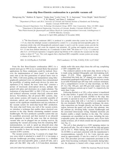
The <strong>vacuum</strong> system (see Fig. 1) consists of a s<strong>in</strong>gle fourway<br />
cross which is attached to a small 8 L/s ion pump, a<br />
four-p<strong>in</strong> feedthrough provid<strong>in</strong>g connections to a rubidium<br />
dispenser and nonevaporable getter, a p<strong>in</strong>ch-off tube, and a<br />
glass <strong>cell</strong> (the BEC <strong>chip</strong> <strong>cell</strong>). A 0.5-mm-thick alum<strong>in</strong>um<br />
nitride wafer (the atom <strong>chip</strong>) closes the <strong>cell</strong> top, complet<strong>in</strong>g<br />
a UHV compatible seal.<br />
The conductor pattern on the atom <strong>chip</strong>, shown <strong>in</strong> Fig. 2,<br />
is made us<strong>in</strong>g standard lithographic and electroplat<strong>in</strong>g techniques<br />
[3–6,9]. When augmented with an external<br />
y-directional bias field, the “U”-shaped wire creates a threedimensional<br />
quadrupole field and the “Z”-shaped wire results<br />
<strong>in</strong> an Ioffe-Pritchard-type (IP) trap with a nonzero m<strong>in</strong>imum.<br />
(For a comprehensive review on <strong>chip</strong> microtraps, see Refs.<br />
[9–11].) The 100-m- and 200-m-wide copper wires can<br />
support cont<strong>in</strong>uous currents up to 4 and 5 A, respectively, for<br />
more than 5 m<strong>in</strong>.<br />
Follow<strong>in</strong>g Reichel et al. [9], a silver mirror is transferred<br />
to the <strong>chip</strong> surface. A quartz <strong>cell</strong> with an <strong>in</strong>ner cross section<br />
of 11 cm is epoxied (Epotek 353ND) to the <strong>chip</strong>; this<br />
assembly is epoxied <strong>in</strong> turn to a UHV glass-to-metal transition<br />
us<strong>in</strong>g a glass disk with a 1 cm bore to compensate for<br />
the size mismatch. With this assembly technique, the atom<strong>chip</strong><br />
connections are brought directly out from the <strong>vacuum</strong><br />
region, between the quartz <strong>cell</strong> and the <strong>chip</strong> substrate, <strong>in</strong>to<br />
the ambient air, obviat<strong>in</strong>g bulky <strong>vacuum</strong> feedthroughs and<br />
the associated <strong>in</strong>tra<strong>vacuum</strong> wir<strong>in</strong>g. Standard electronic p<strong>in</strong><br />
headers enable a simple <strong>in</strong>terface to the <strong>chip</strong>. The various<br />
components are assembled on the cross, <strong>in</strong>clud<strong>in</strong>g the nonevaporable<br />
getter, the rubidium dispenser, and a Pyrex helix<br />
(made <strong>in</strong>-house), all of which extend <strong>in</strong>to the glass transition<br />
(see Fig. 1).<br />
The <strong>cell</strong> is then attached to a UHV pump<strong>in</strong>g station via<br />
the p<strong>in</strong>ch-off tube. The <strong>cell</strong> is baked with the <strong>chip</strong> and quartz<br />
<strong>cell</strong> at 150 °C. While bak<strong>in</strong>g, the getter (SAES ST172/HI/<br />
16-10/300C) is activated consistent with the manufacturer’s<br />
recommendations, typically 5 A for 3-m<strong>in</strong> <strong>in</strong>tervals separated<br />
by approximately 15 m<strong>in</strong> for a total of 15 m<strong>in</strong> activation.<br />
This procedure prevents components proximate to the<br />
getter from becom<strong>in</strong>g overheated. Occasionally dur<strong>in</strong>g bakeout,<br />
the dispenser is heated with a large current 6 A for<br />
1050-2947/2004/70(5)/053606(4)/$22.50 70 053606-1<br />
©2004 The American Physical Society
DU et al. PHYSICAL REVIEW A 70, 053606 (2004)<br />
FIG. 2. The atom <strong>chip</strong> and its wire pattern. Hatch marks <strong>in</strong>dicate<br />
placement of the <strong>cell</strong> (outside edges) on the <strong>chip</strong>. (a) View of the<br />
whole <strong>chip</strong> pattern; (b) center detail of wires where the BEC is<br />
produced. The U wire (I U , 200 m wide) is used to create <strong>chip</strong><br />
MOT, and the Z wire (shown <strong>in</strong> gray, I Z , 100 m wide) is used to<br />
create an IP type magnetic trap by apply<strong>in</strong>g a y-bias field. The other<br />
wires seen <strong>in</strong> (a) are not used <strong>in</strong> this experiment.<br />
FIG. 1. Portable m<strong>in</strong>iature <strong>vacuum</strong> <strong>cell</strong> for the production of a<br />
<strong>chip</strong> BEC. (a) Complete <strong>vacuum</strong> <strong>cell</strong> system, (b) detail of <strong>cell</strong><br />
assembly.<br />
30 s periods. After bakeout, the small ion pump 8 L/s is<br />
turned on and the BEC <strong>cell</strong> is p<strong>in</strong>ched-off from the pump<strong>in</strong>g<br />
station. Gauge pressure on the station side of the p<strong>in</strong>ch-off<br />
tube before p<strong>in</strong>ch-off is below 310 −11 torr. Shortly after<br />
p<strong>in</strong>ch-off, the small ion pump current is below m<strong>in</strong>imum<br />
readout, <strong>in</strong>dicat<strong>in</strong>g a pressure of less than 110 −10 torr. After<br />
p<strong>in</strong>ch-off, the BEC <strong>cell</strong> <strong>vacuum</strong> system is <strong>portable</strong> with<br />
an approximate size of 303015 cm. The <strong>cell</strong> system is<br />
then fitted <strong>in</strong>to a relatively small, fiber-coupled optical bench<br />
with the various optical beams, cameras, and magnetic coils<br />
prealigned to accept the <strong>cell</strong>.<br />
To achieve large atom number <strong>in</strong> the magneto-optical trap<br />
(MOT) and to meet the UHV requirements of <strong>Bose</strong>-<strong>E<strong>in</strong>ste<strong>in</strong></strong><br />
<strong>condensation</strong>, we rapidly modulate the rubidium partial pressure<br />
us<strong>in</strong>g light-<strong>in</strong>duced atomic desorption (LIAD) [13–15]<br />
us<strong>in</strong>g two uv lamps (Norland 5011, 75W) placed 7 cm from<br />
the <strong>cell</strong>. We use mirror MOT lifetime measurements as an<br />
<strong>in</strong>dication of the pressure <strong>in</strong> the <strong>cell</strong>. The lifetime is measured<br />
by turn<strong>in</strong>g off the uv lamps and fitt<strong>in</strong>g the decay<strong>in</strong>g<br />
MOT florescence to an exponential. Typical measured lifetimes<br />
are on the order of 30 s. We verify the MOT lifetime is<br />
not determ<strong>in</strong>ed by the Rb pressure decay after the LIAD<br />
load<strong>in</strong>g. This is done by not<strong>in</strong>g the number loaded <strong>in</strong>to the<br />
MOT after <strong>in</strong>troduc<strong>in</strong>g a delay between uv lamp turn-off and<br />
MOT field turn-on. By this method, we observe the Rb partial<br />
pressure <strong>in</strong> the <strong>cell</strong> decays very rapidly compared to the<br />
053606-2
ATOM-CHIP BOSE-EINSTEIN CONDENSATION IN A… PHYSICAL REVIEW A 70, 053606 (2004)<br />
FIG. 3. <strong>Bose</strong>-<strong>E<strong>in</strong>ste<strong>in</strong></strong> <strong>condensation</strong> is observed. (a) Absorption images are taken after a 5 ms time of flight (TOF) with different f<strong>in</strong>al rf<br />
frequencies. From left to right: (1) =3.5 MHz, N=4210 3 , T=4.4 K, 610 −4 ; (2) =3.0 MHz, N=2010 3 , T=1.4 K, <br />
710 −3 ; (3) =2.9 MHz, N=1010 3 , T=515 nK, 10 −1 ; (4) =2.85 MHz, N=310 3 , T=230 nK, 10. (b) TOF images of<br />
BEC cloud after release with f<strong>in</strong>al rf frequency =2.85 MHz. From left to right: TOF (1) t=1 ms, (2) t=3 ms, (3) t=5 ms, (4) t=7 ms, and<br />
(5) t=9 ms. The nonisotropic shape dur<strong>in</strong>g TOF is a key signature of BEC. [The images <strong>in</strong> (a) are vertically offset relative to (b) no.3so<br />
that they are centered.]<br />
MOT lifetime, and thus the MOT lifetime is determ<strong>in</strong>ed by<br />
the background pressure <strong>in</strong> the <strong>cell</strong>. From the MOT lifetime,<br />
we <strong>in</strong>fer the background pressure <strong>in</strong> the absence of the uv<br />
sources to be 10 −10 torr. From the MOT load<strong>in</strong>g 1/e time<br />
1 s, we estimate the uv light-<strong>in</strong>duced pressure <strong>in</strong>crease to<br />
be a factor of 30.<br />
We use a mirror-MOT [12] for the first stage of cool<strong>in</strong>g<br />
and trapp<strong>in</strong>g. The laser powers of cool<strong>in</strong>g and repump<strong>in</strong>g<br />
beams are 30 mW and 6 mW, respectively, with a beam diameter<br />
of 8 mm. The MOT is loaded by apply<strong>in</strong>g LIAD for<br />
3 s to <strong>in</strong>crease the rubidium vapor pressure followed by a 5 s<br />
hold<strong>in</strong>g time after uv light exposure to improve the pressure<br />
<strong>in</strong> the <strong>cell</strong>. The MOT loaded <strong>in</strong> this way typically traps about<br />
6–710 6 87 Rb atoms with a temperature of 200 K,<br />
2 mm away from the surface. The atoms then undergo a<br />
compressed MOT (CMOT) stage: the cool<strong>in</strong>g laser red detun<strong>in</strong>g<br />
jumps from 10 MHz to 23 MHz and repump<strong>in</strong>g<br />
power is reduced from 6 mW to 100 W, followed by<br />
ramp<strong>in</strong>g the quadrupole field gradient from<br />
14 G/cm to 21 G/cm <strong>in</strong> 20 ms. At the same time, by adjust<strong>in</strong>g<br />
bias fields, the atoms are moved toward the surface<br />
where the quadruple field is replaced with the field generated<br />
by the U wire (I U =2 A and B y =1 G). After 8 ms <strong>in</strong> the U<br />
wire <strong>chip</strong> CMOT, the atoms have a temperature of 100 K.<br />
We then apply 1.7 ms of polarization gradient cool<strong>in</strong>g by<br />
<strong>in</strong>creas<strong>in</strong>g the cool<strong>in</strong>g laser red detun<strong>in</strong>g to 70 MHz and<br />
switch<strong>in</strong>g off all magnetic fields. This further cools atoms to<br />
20 K. No substantial atom loss is observed dur<strong>in</strong>g the<br />
MOT transfer and cool<strong>in</strong>g steps.<br />
After cool<strong>in</strong>g and trapp<strong>in</strong>g, we optically pump the atoms<br />
<strong>in</strong>to the F=2,m F =2 state <strong>in</strong> preparation for load<strong>in</strong>g <strong>in</strong>to the<br />
Z trap. About 2.5–310 6 atoms are loaded <strong>in</strong>to the Z trap<br />
by switch<strong>in</strong>g I Z =4 A and B y =14 G with<strong>in</strong> 10 ms. Immediately<br />
after the load<strong>in</strong>g, the x,y,z bias fields ramp from<br />
0,14,0 G to −4,60,0 G with<strong>in</strong> 100 ms. The magnetic<br />
trap lifetime is about 3–5 s. The approximate factor of 10<br />
difference between the MOT lifetime and the magnetic trap<br />
lifetime is caused by the difference of trap depth [18,19].<br />
After compression, we commence forced evaporation by the<br />
application of an rf field. At the same time, the trap is further<br />
compressed by reduc<strong>in</strong>g I Z from 4 A to 2.75 A <strong>in</strong> 2 s. The<br />
f<strong>in</strong>al trap position is 82 m away from the surface with trap<br />
frequencies of 23,3600,3600 Hz. Forced rf evaporation<br />
takes place through four logarithmic sweeps. The first rf<br />
sweep starts from 45 MHz to 13 MHz for 2.46 s. It is then<br />
followed by a 1 s sweep from 13 MHz to 5 MHz, a 500 ms<br />
sweep from 5 MHz to 3.5 MHz, and a f<strong>in</strong>al 250 ms sweep<br />
from 3.5 MHz to 2.85 MHz. At the end of the f<strong>in</strong>al sweep,<br />
we observe a <strong>Bose</strong>-<strong>E<strong>in</strong>ste<strong>in</strong></strong> condensate of 2000 87 Rb atoms<br />
at a transition temperature of about 300 nK [Fig. 3(a)]. As<br />
shown <strong>in</strong> Fig. 3(b), the anisotropic shape dur<strong>in</strong>g 9 ms TOF<br />
(time of flight) is a clear signature of a <strong>Bose</strong>-<strong>E<strong>in</strong>ste<strong>in</strong></strong> condensate.<br />
A4 K/s heat<strong>in</strong>g rate that is <strong>in</strong>dependent of density leads<br />
to a 100 ms BEC lifetime. Lower<strong>in</strong>g the trap frequencies by<br />
chang<strong>in</strong>g I Z from 2.75 A to 0.65 A, and B y from<br />
60 G to 14.5 G, reduces the heat<strong>in</strong>g rate to 0.5 K/s,<br />
which corresponds to a BEC lifetime of 300 ms. The total<br />
atom number <strong>in</strong> the trap is conserved dur<strong>in</strong>g the BEC lifetime.<br />
This suggests the heat<strong>in</strong>g is not caused by three-body<br />
recomb<strong>in</strong>ation, but by another mechanism.<br />
Two additional remarks are perhaps appropriate. First, <strong>in</strong><br />
many BEC <strong>vacuum</strong> systems a titanium sublimation pump is<br />
utilized to help achieve and ma<strong>in</strong>ta<strong>in</strong> ultrahigh <strong>vacuum</strong>. The<br />
effective pump<strong>in</strong>g of hydrogen is particularly important<br />
where heated rubidium dispensers are used because they also<br />
release substantial amounts of hydrogen. Our work suggests<br />
that the nonevaporable getter can serve the same purpose as<br />
the sublimation pump, at least <strong>in</strong> these small <strong>cell</strong>s. The nonevaporable<br />
getter is rated by the manufacturer to have a<br />
pump<strong>in</strong>g speed of 1 L/s and a large hydrogen capacity,<br />
1 torr L at room temperature. Second, our first <strong>cell</strong> designs<br />
with quartz <strong>cell</strong>s were unable to obta<strong>in</strong> sufficient atom numbers<br />
<strong>in</strong> the MOT through the LIAD technique. We <strong>in</strong>troduced<br />
a Pyrex helix <strong>in</strong>to the <strong>cell</strong> to <strong>in</strong>crease the surface area from<br />
053606-3
DU et al. PHYSICAL REVIEW A 70, 053606 (2004)<br />
which to desorb rubidium. Pyrex was chosen because prior<br />
LIAD experiments [13–15] were successfully performed us<strong>in</strong>g<br />
Pyrex. The helix shape, made <strong>in</strong>-house, was chosen arbitarily.<br />
Probably any shape that <strong>in</strong>creases the surface area<br />
for desorption will suffice. In the hopes of elim<strong>in</strong>at<strong>in</strong>g the<br />
bulky uv lamps, we attempted LIAD us<strong>in</strong>g blue LED’s as<br />
well as laser light at =532 nm 100 mW and 408 nm<br />
10 mW. None were as effective as the <strong>in</strong>candescent lamps<br />
(150 W total). We were able to capture rubidium atoms even<br />
with the LED’s, suggest<strong>in</strong>g the possibility of a more efficient<br />
and compact LIAD source.<br />
The achievement of BEC demonstrates the viability of<br />
small and <strong>portable</strong> <strong>chip</strong>-based <strong>vacuum</strong> <strong>cell</strong>s for atom <strong>chip</strong><br />
applications. Our results suggest that a BEC suitable <strong>vacuum</strong><br />
<strong>cell</strong> can be made substantially smaller still. In particular, all<br />
of the key elements except for the ion pump reside with<strong>in</strong> the<br />
glass-to-metal transition region, as shown <strong>in</strong> Fig. 1(b). The<br />
8 L/s ion pump is <strong>in</strong> fact already limited by the <strong>cell</strong> structure<br />
itself to a pump<strong>in</strong>g speed of about 2 1 L/s. Thus, we expect<br />
it is possible to reduce the total volume of the <strong>vacuum</strong> system<br />
to well less than 0.5 L, dom<strong>in</strong>ated by a small ion pump.<br />
As the <strong>cell</strong> itself becomes smaller, many of the practical<br />
parameters also improve, such as the size and power requirements<br />
of the magnetic coils. On the other hand, the MOT<br />
capture volume is small, result<strong>in</strong>g <strong>in</strong> a small MOT and subsequent<br />
small BEC. It should be noted that a small BEC does<br />
not prohibit its utility [16,17].<br />
In summary, we have successfully demonstrated <strong>Bose</strong>-<br />
<strong>E<strong>in</strong>ste<strong>in</strong></strong> <strong>condensation</strong> <strong>in</strong> a compact and <strong>portable</strong> <strong>vacuum</strong><br />
system. The size reduction and simplification are largely due<br />
to the techniques that allow all cool<strong>in</strong>g steps to take place <strong>in</strong><br />
a s<strong>in</strong>gle small chamber and the <strong>chip</strong>-based electrical<br />
feedthroughs, which greatly facilitate <strong>chip</strong> connections. In<br />
our experiments, we have succeeded <strong>in</strong> realiz<strong>in</strong>g a “plug-<strong>in</strong>”<br />
concept where the atom <strong>chip</strong> <strong>vacuum</strong> <strong>cell</strong> is plugged <strong>in</strong>to an<br />
exist<strong>in</strong>g optical and electronic system. Through this concept,<br />
we hope that atom <strong>chip</strong> development and experiments can<br />
proceed more rapidly.<br />
The authors thank E. A. Cornell, D. J<strong>in</strong>, Y. J. Wang, T.<br />
Kishimoto, S. Inoyoe, and J. Goldw<strong>in</strong> for helpful discussions.<br />
This work was supported <strong>in</strong> part by ARO and the<br />
Office of the Secretary of Defense through a MURI program<br />
<strong>in</strong> Ultracold <strong>Atom</strong> Optics Science and Technology (Grant<br />
No. DAAD19-00-1-0163); this work was also made possible<br />
by fund<strong>in</strong>g from the Office of Naval Research (Grant No.<br />
N00014-03-1-0551) and the National Science Foundation<br />
(Grant No. PHY-0096822). M.B.S. gratefully acknowledges<br />
support from the NSF-IGERT program. D.Z.A. gratefully acknowledges<br />
support of the Alexander von Humboldt Foundation.<br />
[1] M. H. Anderson, J. R. Ensher, M. R. Matthews, C. E. Wieman,<br />
and E. A. Cornell, Science 269, 198 (1995).<br />
[2] K. B. Davis, M.-O. Mewes, M. R. Andrews, N. J. van Druten,<br />
D. S. Durfee, D. M. Kurn, and W. Ketterle, Phys. Rev. Lett.<br />
75, 3969 (1995).<br />
[3] D. Müller, D. Z. Anderson, R. J. Grow, P. D. D. Schw<strong>in</strong>dt, and<br />
E. A. Cornell, Phys. Rev. Lett. 83, 5194 (1999).<br />
[4] N. H. Dekker, C. S. Lee, V. Lorent, J. H. Thywissen, S. P.<br />
Smith, M. Drndi, R. M. Westervelt, and M. Prentiss, Phys.<br />
Rev. Lett. 84, 1124 (2000).<br />
[5] D. Müller et al., Opt. Lett. 25, 1382 (2000).<br />
[6] D. Cassettari, B. Hessmo, R. Folman, T. Maier, and J.<br />
Schmiedmayer, Phys. Rev. Lett. 85, 5483 (2000).<br />
[7] W. Hänsel, P. Hommelhoff, T. W. Hänsch, and J. Reichel, Nature<br />
(London) 413, 498 (2001).<br />
[8] H. Ott, J. Fortagh, G. Schlotterbeck, A. Grossmann, and C.<br />
Zimmermann, Phys. Rev. Lett. 87, 230401 (2001).<br />
[9] J. Reichel, W. Hänsel, P. Hommelhoff, and T. W. Hänsch,<br />
Appl. Phys. B: Lasers Opt. 72, 81(2001).<br />
[10] R. Folman, P. Krüger, and J. Schmiedmayer, J. Denschlag, and<br />
C. Henkel, Adv. At., Mol., Opt. Phys. 48, 263 (2002).<br />
[11] J. Reichel, Appl. Phys. B: Lasers Opt. 74, 469 (2002).<br />
[12] J. Reichel, W. Hänsel, and T. W. Hänsch, Phys. Rev. Lett. 83,<br />
3398 (1999).<br />
[13] B. P. Anderson and M. A. Kasevich, Phys. Rev. A 63, 023404<br />
(2001).<br />
[14] E. B. Alexandrov, M. V. Balabas, D. Budkler, D. English, D. F.<br />
Kimball, C.-H. Li, and V. V. Yashchuk, Phys. Rev. A 66,<br />
042903 (2002).<br />
[15] S. N. Autov, R. Calabrese, V. Guidi, B. Mai, A. G. Rudavets,<br />
E. Scansani, L. Tomassetti, V. Biancalana, A. Burchianti, C.<br />
Mar<strong>in</strong>elli, E. Mariotti, L. Moi, and S. Veronesi, Phys. Rev. A<br />
67, 053401 (2003).<br />
[16] Y. L<strong>in</strong>, I. Teper, C. Ch<strong>in</strong>, and V. Vuletic, Phys. Rev. Lett. 92,<br />
050404 (2004).<br />
[17] P. Treutle<strong>in</strong>, P. Hommelhoff, T. Ste<strong>in</strong>metz, T. W. Hänsch, and<br />
J. Reichel, Phys. Rev. Lett. 92, 203005 (2004).<br />
[18] J. E. Bjorkholm, Phys. Rev. A 38, 1599 (1988).<br />
[19] C. Monroe, W. Swann, H. Rob<strong>in</strong>son, and C. Wieman, Phys.<br />
Rev. Lett. 65, 1571 (1990).<br />
053606-4
