A Practical Guide to SPM
A Practical Guide to SPM
A Practical Guide to SPM

Create successful ePaper yourself
Turn your PDF publications into a flip-book with our unique Google optimized e-Paper software.
20<br />
protein, attached <strong>to</strong> the tip, unfolds, often one molecular bond at a<br />
time. The resulting force-distance curve will show a series of snap-back<br />
points in the retraction curve, each representing the breaking of a<br />
chemical bond.<br />
Surface Modification Techniques<br />
Normally, an <strong>SPM</strong> is used <strong>to</strong> image a surface without altering it.<br />
However, AFMs and STMs can also be used <strong>to</strong> deliberately modify a<br />
surface. This modification is accomplished with specialized <strong>SPM</strong><br />
software that provides additional ways <strong>to</strong> control the motion of the<br />
scanner and thus the probe or the sample.<br />
Nanolithography<br />
Nanolithography is “drawing” a nanometer-scale pattern on a sample<br />
surface using an <strong>SPM</strong> tip. This can be done by mechanically scribing<br />
the surface by applying excessive force with an AFM tip or by<br />
applying highly localized electric fields <strong>to</strong> oxidize the surface with an<br />
AFM or STM tip. Nanolithography software allows the user <strong>to</strong> create<br />
programs that control tip movements <strong>to</strong> draw a pre-defined pattern or<br />
<strong>to</strong> draw as freely as when writing by hand with a pen — point-andclick<br />
nanolithography (Figure 6-3). Nanolithography with an AFM or<br />
STM includes recipe-driven modes, or modes in which the nanolithographed<br />
pattern is that of a bitmap or vec<strong>to</strong>r-based graphic object<br />
imported in<strong>to</strong> the <strong>SPM</strong> software.<br />
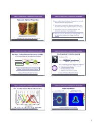
Figure 6-3. Point-and-click nanolithography.<br />
Nanoindentation, Nanoscratching, Wear Testing<br />
Nanoindentation is a way of measuring mechanical properties by<br />
nanoindenting a sample with an AFM tip (often a hard diamond tip)<br />
<strong>to</strong> investigate hardness. Nanoscratching and wear testing utilize the<br />
same hardware <strong>to</strong> drag a tip across the surface with the explicit intent<br />
of creating and then visualizing scratches, surface de-laminations, etc.<br />
Please see Veeco Instruments’ application notes on this subject.<br />
Nanomanipulation<br />
Nanomanipulation with AFM requires specialized hardware and<br />
software. Advanced software provides the user with flexible control<br />
and measurement of in-plane (X,Y) and out-of-plane (Z) position and<br />
movement of the <strong>SPM</strong> probe, using highly accurate positioning<br />
hardware and feedback schemes. It allows direct, precise<br />
manipulation of nanoscale objects, such as nanotubes and<br />
nanoparticles in the plane of the sample surface, and of objects like<br />
macromolecules in and out of the plane of the sample surface.