A Practical Guide to SPM
A Practical Guide to SPM
A Practical Guide to SPM

Create successful ePaper yourself
Turn your PDF publications into a flip-book with our unique Google optimized e-Paper software.
17<br />
VI. Non-imaging Modes<br />
<strong>SPM</strong>s are most commonly thought of as <strong>to</strong>ols for generating images of<br />
a sample's surface. However, <strong>SPM</strong>s can also be used <strong>to</strong> measure<br />
material properties at a single X,Y point on the sample surface. (In the<br />
<strong>SPM</strong> literature, this is often referred <strong>to</strong> as <strong>SPM</strong> spectroscopy, which we<br />
adopt here, and which is quite different from the traditional definition<br />
of spectroscopy in the sciences.) <strong>SPM</strong>s are also used <strong>to</strong> alter — rather<br />
than measure — the sample surface. Examples include nanolithography,<br />
nanomanipulation, molecular pulling, and nanoindentation.<br />
These non-imaging modes of <strong>SPM</strong>s are increasingly used<br />
in surface science. In this chapter, we describe the most popular nonimaging<br />
<strong>SPM</strong> modes.<br />
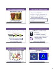
Spectroscopy<br />
Scanning Tunneling Spectroscopy (STS)<br />
A scanning tunneling microscope (STM) can be used as a<br />
spectroscopy <strong>to</strong>ol, probing the electronic properties of a material with<br />
a<strong>to</strong>mic resolution in the X-Y plane of the sample surface. This technique<br />
is called scanning tunneling spectroscopy (STS). By comparison,<br />
traditional spectroscopy techniques like XPS (x-ray pho<strong>to</strong>electron<br />
spectroscopy), UPS (ultraviolet pho<strong>to</strong>electron spectroscopy), and IPES<br />
(inverse pho<strong>to</strong>-emission spectroscopy) detect and average the data<br />
originating from a relatively large area: a few microns <strong>to</strong> a few<br />
millimeters across.<br />
STS studies the local electronic structure of a sample’s surface. The<br />
electronic structure of an a<strong>to</strong>m depends upon its a<strong>to</strong>mic species (e.g.,<br />
whether it is a gallium a<strong>to</strong>m or an arsenic a<strong>to</strong>m) and its local<br />
environment (how many neighboring a<strong>to</strong>ms it has, what kind of a<strong>to</strong>ms<br />
they are, and the symmetry of their distribution).<br />
STS encompasses many methods. For example, at constant tip-sample<br />
separation, we can ramp the bias voltage with the tip positioned over<br />
a feature of interest while recording the tunneling current. This results<br />
in current vs. voltage (I-V) curves, which characterize the electronic<br />
structure at a specific X,Y location. An STM can be set up <strong>to</strong> perform<br />
STS (collect I-V curves) at numerous points across the sample surface,<br />
providing a three-dimensional map similar <strong>to</strong> force volume imaging in<br />
AFM, which is also described in this chapter.<br />
Force Spectroscopy<br />
An AFM can be used as a spectroscopy <strong>to</strong>ol, probing the tip-sample<br />
interaction at a given X,Y location on the sample surface. In <strong>SPM</strong><br />
literature, this is typically called force spectroscopy because the<br />
interaction results in a force (as opposed <strong>to</strong> a current in STS). This<br />
method typically produces a force vs. distance curve, which is a plot<br />
of the force on an AFM cantilever (via the tip) in the Z direction as a<br />
function of the tip-sample separation in Z. Force vs. distance curves<br />
were first used <strong>to</strong> measure the vertical force the AFM tip applies <strong>to</strong> the