Carbon Nanomaterials (PDF)
Carbon Nanomaterials (PDF)
Carbon Nanomaterials (PDF)

You also want an ePaper? Increase the reach of your titles
YUMPU automatically turns print PDFs into web optimized ePapers that Google loves.
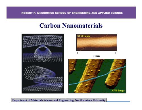
<strong>Carbon</strong> <strong>Nanomaterials</strong><br />
STM Image<br />
7 nm<br />
AFM Image<br />
Department of Materials Science and Engineering, Northwestern University
Fullerenes<br />
• C 60<br />
was established by mass spectrographic analysis by Kroto and Smalley in 1985<br />
• C 60<br />
is called a buckminsterfullerene or buckyball due to resemblance to geodesic<br />
domes designed and built by R. Buckminster Fuller<br />
G. Timp, Nanotechnology, Chapter 7<br />
Department of Materials Science and Engineering, Northwestern University
Endofullerenes<br />
• Endohedral doping of fullerenes leads to the formation of a dipole moment that<br />
influences solubility and other properties.<br />
G. Timp, Nanotechnology, Chapter 7<br />
Department of Materials Science and Engineering, Northwestern University
Electronic Structure of Molecular and Solid C 60<br />
G. Timp, Nanotechnology, Chapter 7<br />
Department of Materials Science and Engineering, Northwestern University
Dangling<br />
Bonds<br />
Single Molecule STM Spectroscopy of C 60<br />
3-D STM Topograph<br />
C 60<br />
70 Å x 70 Å<br />
Structure of C 60<br />
Spectroscopic variation among surface features<br />
Si<br />
dI/dV (A.U.)<br />
1.0<br />
0.8<br />
0.6<br />
0.4<br />
C 60<br />
Si Dangling Bond<br />
H-passivated Si<br />
LUMO peak<br />
Ge<br />
0.2<br />
0.0<br />
-2 -1 0 1 2<br />
Energy (eV)<br />
Calculated local density of states for Si(100)<br />
Department of Materials Science and Engineering, Northwestern University
Rolled Up From Graphene Sheets:<br />
<strong>Carbon</strong> Nanotubes<br />
G. Timp, Nanotechnology, Chapter 7<br />
Department of Materials Science and Engineering, Northwestern University
<strong>Carbon</strong> Nanotube Synthesis:<br />
<strong>Carbon</strong> Arc Discharge<br />
P. G. Collins and Ph. Avouris, Scientific American, 283, 62 (2000).<br />
Department of Materials Science and Engineering, Northwestern University
<strong>Carbon</strong> Nanotube Synthesis:<br />
Chemical Vapor Deposition<br />
P. G. Collins and Ph. Avouris, Scientific American, 283, 62 (2000).<br />
Department of Materials Science and Engineering, Northwestern University
<strong>Carbon</strong> Nanotube Synthesis:<br />
Laser Ablation<br />
P. G. Collins and Ph. Avouris, Scientific American, 283, 62 (2000).<br />
Department of Materials Science and Engineering, Northwestern University
Chirality of <strong>Carbon</strong> Nanotubes<br />
G. Timp, Nanotechnology, Chapter 7<br />
Department of Materials Science and Engineering, Northwestern University
Energy Band Diagrams of <strong>Carbon</strong> Nanotubes<br />
G. Timp, Nanotechnology, Chapter 7<br />
Department of Materials Science and Engineering, Northwestern University
Electrical Properties of Graphite<br />
P. G. Collins and Ph. Avouris, Scientific American, 283, 62 (2000).<br />
Department of Materials Science and Engineering, Northwestern University
Electrical Properties of Straight Nanotubes<br />
P. G. Collins and Ph. Avouris, Scientific American, 283, 62 (2000).<br />
Department of Materials Science and Engineering, Northwestern University
Electrical Properties of Twisted Nanotubes<br />
P. G. Collins and Ph. Avouris, Scientific American, 283, 62 (2000).<br />
Department of Materials Science and Engineering, Northwestern University
Bandgap of Semiconducting Nanotubes<br />
G. Timp, Nanotechnology, Chapter 7<br />
Department of Materials Science and Engineering, Northwestern University
Electrical Properties of MWNTs<br />
• MWNT bandgap is proportional to 1/d At room temperature,<br />
MWNTs behave like metals since d ~ 10 nm<br />
• Only the outermost shell carries current in an undamaged MWNT<br />
Department of Materials Science and Engineering, Northwestern University
Other Properties of SWNTs<br />
P. G. Collins and Ph. Avouris, Scientific American, 283, 62 (2000).<br />
Department of Materials Science and Engineering, Northwestern University
Other Properties of SWNTs<br />
P. G. Collins and Ph. Avouris, Scientific American, 283, 62 (2000).<br />
Department of Materials Science and Engineering, Northwestern University
Nanotubes as Interconnects<br />
P. G. Collins and Ph. Avouris, Scientific American, 283, 62 (2000).<br />
Department of Materials Science and Engineering, Northwestern University
Current Carrying Capacity of MWNTs<br />
Although a cross-sectional view of a MWNT shows several<br />
cylindrical shells, only the outermost shell carries current in<br />
an undamaged MWNT.<br />
Department of Materials Science and Engineering, Northwestern University
Representative MWNT I-V Curve:<br />
8<br />
Current density (x10 13 A/m 2 )<br />
6<br />
4<br />
2<br />
Maximum current density: 6.8 x 10 13 A/m 2<br />
Maximum electric field: 1.6 x 10 7 V/m<br />
0<br />
0<br />
2<br />
4<br />
6 8 10<br />
Electric field (x10 6 V/m)<br />
12<br />
14<br />
16<br />
Maximum current densities of potential interconnect materials:<br />
• Metals: 10 10 –10 12 A/m 2<br />
• Superconductors: J c ~ 10 12 A/m 2<br />
• MWNTs: >5×10 13 A/m 2<br />
Department of Materials Science and Engineering, Northwestern University
Electrically Stressed MWNTs<br />
Before Electrical Stress<br />
After Failure<br />
1 µm 2 AFM image<br />
1 µm 2 AFM image<br />
Experimental method: Monitor the current as a function of time<br />
while stressing the MWNT at a fixed voltage.<br />
Department of Materials Science and Engineering, Northwestern University
Multiwalled <strong>Carbon</strong> Nanotube Failure<br />
P. G. Collins, et al., Phys. Rev. Lett., 86, 3128 (2001).<br />
Department of Materials Science and Engineering, Northwestern University
Device Applications of Nanotube Junctions<br />
G. Timp, Nanotechnology, Chapter 7<br />
Department of Materials Science and Engineering, Northwestern University
Engineering <strong>Carbon</strong> Nanotubes<br />
Using Electrical Breakdown<br />
P. G. Collins, et al., Science, 292, 706 (2001).<br />
Department of Materials Science and Engineering, Northwestern University
Engineering <strong>Carbon</strong> Nanotubes<br />
Using Electrical Breakdown<br />
P. G. Collins, et al., Science, 292, 706 (2001).<br />
Department of Materials Science and Engineering, Northwestern University
Electronic Applications of SWNTs<br />
Field Effect Transistors<br />
Field Emission Displays<br />
P. G. Collins and Ph. Avouris, Scientific American, 283, 62 (2000).<br />
Department of Materials Science and Engineering, Northwestern University
Nanotube Complementary Logic<br />
V. Derycke, et al., Nano Letters, 1, 453 (2001).<br />
Department of Materials Science and Engineering, Northwestern University
Nanotube Complementary Logic<br />
V. Derycke, et al., Nano Letters, 1, 453 (2001).<br />
Department of Materials Science and Engineering, Northwestern University
Other Applications of Nanotubes<br />
P. G. Collins and Ph. Avouris, Scientific American, 283, 62 (2000).<br />
Department of Materials Science and Engineering, Northwestern University
Other Applications of Nanotubes<br />
P. G. Collins and Ph. Avouris, Scientific American, 283, 62 (2000).<br />
Department of Materials Science and Engineering, Northwestern University
Density of States<br />
In general, the density of states in d-dimensions is:<br />
⎛<br />
D(<br />
E)<br />
= ⎜<br />
⎝<br />
L ⎞<br />
⎟<br />
2π<br />
⎠<br />
d<br />
∫<br />
δ ( k(<br />
E)<br />
−k)<br />
dk<br />
∇ ( E)<br />
k<br />
d<br />
At band edges, ∇ ( E)<br />
= 0<br />
k<br />
van Hove singularities in the density of states<br />
T. W. Odom, et al., J. Phys. Chem. B, 104, 2794 (2000).<br />
Department of Materials Science and Engineering, Northwestern University
Nanotube 1-D Density of States<br />
The van Hove singularities assume different forms based on the<br />
dimensionality of the system:<br />
The 1-D nature of nanotubes leads to peaks in the density of states.<br />
T. W. Odom, et al., J. Phys. Chem. B, 104, 2794 (2000).<br />
Department of Materials Science and Engineering, Northwestern University
STM Measurements of Nanotube<br />
van Hove Singularities<br />
J. W. G. Wilder, et al., Nature, 391, 59 (1998).<br />
Department of Materials Science and Engineering, Northwestern University
Implications of van Hove Singularities<br />
for Nanotube Optical Properties<br />
S. M. Bachilo, et al., Science, 298, 2361 (2002).<br />
Department of Materials Science and Engineering, Northwestern University
Separating <strong>Carbon</strong> Nanotubes in Solution<br />
M. J. O’Connell, et al., Science, 297, 593 (2002).<br />
Department of Materials Science and Engineering, Northwestern University
Band Gap Absorption and Fluorescence from<br />
Individual Single-Walled <strong>Carbon</strong> Nanotubes<br />
M. J. O’Connell, et al., Science, 297, 593 (2002).<br />
Department of Materials Science and Engineering, Northwestern University
Excitation at the E 22 Transition<br />
M. J. O’Connell, et al., Science, 297, 593 (2002).<br />
Department of Materials Science and Engineering, Northwestern University
Structure-Assigned Optical Spectra<br />
S. M. Bachilo, et al., Science, 298, 2361 (2002).<br />
Department of Materials Science and Engineering, Northwestern University
Ambipolar <strong>Carbon</strong> Nanotube FET<br />
Fig. 1. (A) Schematic diagram of the<br />
ambipolar s-SWNT device structure. (B)<br />
Electrical characterization of a typical<br />
ambipolar device. A plot of the drain<br />
current versus Vg for a grounded source<br />
and a small drain potential of1Vis shown.<br />
The data indicate ambipolar behavior. (C)<br />
Plot of the drain current versus Vd for a<br />
grounded source and a gate potential of 5<br />
V for the device used in the optical<br />
measurements. The inset shows the data<br />
on a logarithmic scale. (D) Calculated<br />
band structure for carbon nanotube FET<br />
devices with Vd = 4 V and Vg halfway<br />
between the source and drain voltages.<br />
J. A. Misewich, et al., Science, 300, 783 (2003).<br />
Department of Materials Science and Engineering, Northwestern University
Infrared Emission from an Ambipolar Nanotube FET<br />
Fig. 2. Optical emission from an ambipolar<br />
carbon nanotube FET detected with an IR<br />
camera. The upper plane is a color-coded IR<br />
image of the carbon nanotube FET. The<br />
contact pads and thin wires leading to the<br />
carbon nanotube channel are shown in yellow.<br />
The lower plane is the surface plot of the IR<br />
emission image taken under conditions of<br />
simultaneous e– and h+ injection into the<br />
carbon nanotube. The emission was localized<br />
at the position of the carbon nanotube. (Inset)<br />
SEM showing the device structure in the<br />
region of the nanotube emitter.<br />
J. A. Misewich, et al., Science, 300, 783 (2003).<br />
Department of Materials Science and Engineering, Northwestern University
Characterization of Stimulated Emission<br />
from Encapsulated SWNTs<br />
M. S. Arnold, et al., Nano Letters, 3, 1549 (2003).<br />
Department of Materials Science and Engineering, Northwestern University
Filter<br />
Pulsed pump from Ti:sapphire<br />
laser (300 fs pulse width)<br />
Probe from CW<br />
fiber laser (λ=1053 nm)<br />
60dB<br />
ESA or oscilloscope<br />
Sample (stirred)<br />
Experimental setup<br />
Probe modulation [dBm]<br />
-20<br />
Pump & probe on<br />
-40<br />
Probe on<br />
-60<br />
-80<br />
Pump on<br />
-100<br />
75.72 75.74 75.76 75.78 75.80<br />
RF Frequency [MHz]<br />
Stimulated emission [mV]<br />
30<br />
20<br />
10<br />
0<br />
-10<br />
0 10 20 30 40 50<br />
Time [ns]<br />
Probe modulation in frequency domain<br />
Temporal response of probe modulation<br />
Department of Materials Science and Engineering, Northwestern University
Effect of Aggregation and pH<br />
• Aggregation of isolated nanotubes<br />
by lyophilization and re-suspension<br />
drastically reduces probe modulation<br />
intensity by a factor of 122.<br />
• Photobleaching disappears at acidic<br />
pH and is reversibly restored at<br />
neutral and basic pH, consistent with<br />
protonation of nanotube sidewalls at<br />
acidic pH.<br />
M. S. Arnold, et al., Nano Letters, 3, 1549 (2003).<br />
Department of Materials Science and Engineering, Northwestern University
Pump Spectral Dependence<br />
• The measured E 22 transition<br />
width of 65 meV is consistent with<br />
fast electron-electron scattering on<br />
the 300 fs time scale.<br />
• The feature near 1.4 eV is likely<br />
due to a Raman effect (the<br />
measured difference between<br />
pump and probe energies is ~<br />
1600 cm -1 , which matches the G-<br />
band Raman mode in SWNTs).<br />
M. S. Arnold, et al., Nano Letters, 3, 1549 (2003).<br />
Department of Materials Science and Engineering, Northwestern University
Probe Spectral Dependence<br />
• The probe modulation<br />
spectrum is slightly red-shifted<br />
from the absorbance spectrum<br />
by 45 cm -1 .<br />
• From a Lorentzian fit, the<br />
width of the E 11 transition is<br />
only 10 meV compared with 65<br />
meV as measured for the E 22<br />
transition.<br />
M. S. Arnold, et al., Nano Letters, 3, 1549 (2003).<br />
Department of Materials Science and Engineering, Northwestern University
Polarization Dependence<br />
Co-polarized pump and probe lead to greater photobleaching than<br />
cross-polarized as expected for a 1-D system.<br />
M. S. Arnold, et al., Nano Letters, 3, 1549 (2003).<br />
Department of Materials Science and Engineering, Northwestern University
Pump Saturation Effects<br />
• At low pump intensities below 10<br />
W/cm 2 , linear behavior is observed.<br />
• Saturation of the probe modulation<br />
is consistent with:<br />
‣ Increased multi-particle Auger<br />
recombination for large carrier<br />
densities.<br />
‣ Exciton-exciton annihilation<br />
effects.<br />
‣ Saturation and filling of a finite<br />
number of states.<br />
M. S. Arnold, et al., Nano Letters, 3, 1549 (2003).<br />
Department of Materials Science and Engineering, Northwestern University
Probe Saturation Effects<br />
• x S corresponds to the probe intensity<br />
for which the rate of stimulated<br />
recombination is equal to the intrinsic<br />
rate of recombination.<br />
•An increase in x s at large pump<br />
intensities is consistent with an increase<br />
in the effective interband recombination<br />
rate due to enhanced Auger<br />
recombination for large carrier densities.<br />
M. S. Arnold, et al., Nano Letters, 3, 1549 (2003).<br />
Department of Materials Science and Engineering, Northwestern University
Degenerate Pump-Probe Measurements<br />
Normalized modulation<br />
1.0<br />
0.8<br />
0.6<br />
0.4<br />
0.2<br />
Decay<br />
E 11<br />
E 22<br />
Degenerate pump-probe<br />
optical setup.<br />
0.0<br />
0<br />
40<br />
80<br />
delay (ps)<br />
120<br />
160<br />
Time-resolved relaxation at E 11 (975 nm)<br />
and E 22 (740 nm) optical transitions.<br />
Department of Materials Science and Engineering, Northwestern University
Temporal Relaxation at E 11<br />
Semi-log relaxation at E 11 (975 nm)<br />
Department of Materials Science and Engineering, Northwestern University
An Estimate of the Optical Gain<br />
~ 10%<br />
instantaneous<br />
decrease in<br />
absorption<br />
To reach optical<br />
transparency,<br />
SWNTs need to<br />
be separated<br />
by electronic<br />
bandstructure<br />
Department of Materials Science and Engineering, Northwestern University
DNA Encapsulated SWNTs<br />
M. Zheng, et al., Nature Mat., 2, 338 (2003). M. Zheng, et al., Science, 302, 1545 (2003).<br />
Department of Materials Science and Engineering, Northwestern University
SPM of DNA Encapsulated<br />
SWNTs on Silicon Surfaces<br />
Ambient AFM of ssDNA-NT on Si(111)-1x1:H<br />
UHV STM of ssDNA-NT on Si(100)-2x1:H<br />
Pitch ~12 nm<br />
Pitch ~12 nm<br />
Atomic force microscopy, scanning tunneling microscopy<br />
Department of Materials Science and Engineering, Northwestern University
Optical Absorption Spectra for<br />
DNA Encapsulated SWNTs<br />
Optical absorbance<br />
spectrum:<br />
Department of Materials Science and Engineering, Northwestern University
Density of DNA Encapsulated SWNTs<br />
Density of SWNTs in vacuum:<br />
ρ NT<br />
:=<br />
4 ρ s<br />
D<br />
Density of DNA encapsulated SWNTs:<br />
ρ s<br />
π D +<br />
ρ NT<br />
:=<br />
ρ s<br />
= areal density of graphite = 7.66×10 -8 g/cm 2<br />
ρ ext<br />
= volume density of hydrated DNA in iodixanol = 1.12 g/cm 3<br />
ρ π ⎛ ⎛<br />
ext ⎝ ⎜ ⎜<br />
⎝<br />
π ⎛ ⎝ ⎜<br />
D<br />
2<br />
D<br />
2<br />
+ t<br />
⎞<br />
⎟<br />
⎠<br />
+ t<br />
⎞<br />
⎟<br />
⎠<br />
2<br />
2<br />
−<br />
D 2<br />
4<br />
⎞<br />
⎟<br />
⎠<br />
M. S. Arnold, et al., Nano Letters, 5, 713 (2005).<br />
Department of Materials Science and Engineering, Northwestern University
Density Gradient Centrifugation of<br />
DNA Encapsulated SWNTs<br />
Density of DNA encapsulated SWNTs:<br />
1.11 – 1.17 g/cm 3<br />
→ DNA hydration layer thickness of 2 – 3 nm<br />
M. S. Arnold, et al., Nano Letters, 5, 713 (2005).<br />
Department of Materials Science and Engineering, Northwestern University
Separation of DNA Encapsulated<br />
SWNTs by Diameter<br />
M. S. Arnold, et al., Nano Letters, 5, 713 (2005).<br />
Department of Materials Science and Engineering, Northwestern University
Correlating Diameter and Density<br />
• Density of DNA encapsulated SWNTs increases with increasing diameter.<br />
• Separation is most effective at small diameters.<br />
M. S. Arnold, et al., Nano Letters, 5, 713 (2005).<br />
Department of Materials Science and Engineering, Northwestern University