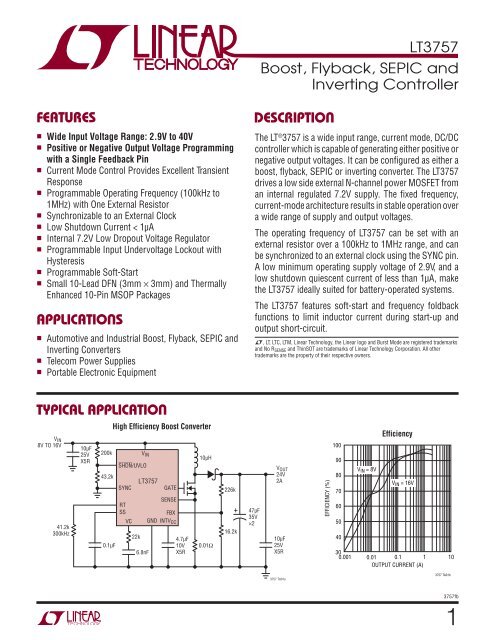
LT3757 - Boost, Flyback, SEPIC and Inverting Controller
LT3757 - Boost, Flyback, SEPIC and Inverting Controller
LT3757 - Boost, Flyback, SEPIC and Inverting Controller

You also want an ePaper? Increase the reach of your titles
YUMPU automatically turns print PDFs into web optimized ePapers that Google loves.
<strong>LT3757</strong><br />
<strong>Boost</strong>, <strong>Flyback</strong>, <strong>SEPIC</strong> <strong>and</strong><br />
<strong>Inverting</strong> <strong>Controller</strong><br />
Features<br />
n Wide Input Voltage Range: 2.9V to 40V<br />
n Positive or Negative Output Voltage Programming<br />
with a Single Feedback Pin<br />
n Current Mode Control Provides Excellent Transient<br />
Response<br />
n Programmable Operating Frequency (100kHz to<br />
1MHz) with One External Resistor<br />
n Synchronizable to an External Clock<br />
n Low Shutdown Current < 1µA<br />
n Internal 7.2V Low Dropout Voltage Regulator<br />
n Programmable Input Undervoltage Lockout with<br />
Hysteresis<br />
n Programmable Soft-Start<br />
n Small 10-Lead DFN (3mm × 3mm) <strong>and</strong> Thermally<br />
Enhanced 10-Pin MSOP Packages<br />
Applications<br />
n Automotive <strong>and</strong> Industrial <strong>Boost</strong>, <strong>Flyback</strong>, <strong>SEPIC</strong> <strong>and</strong><br />
<strong>Inverting</strong> Converters<br />
n Telecom Power Supplies<br />
n Portable Electronic Equipment<br />
Description<br />
The LT ® 3757 is a wide input range, current mode, DC/DC<br />
controller which is capable of generating either positive or<br />
negative output voltages. It can be configured as either a<br />
boost, flyback, <strong>SEPIC</strong> or inverting converter. The <strong>LT3757</strong><br />
drives a low side external N-channel power MOSFET from<br />
an internal regulated 7.2V supply. The fixed frequency,<br />
current-mode architecture results in stable operation over<br />
a wide range of supply <strong>and</strong> output voltages.<br />
The operating frequency of <strong>LT3757</strong> can be set with an<br />
external resistor over a 100kHz to 1MHz range, <strong>and</strong> can<br />
be synchronized to an external clock using the SYNC pin.<br />
A low minimum operating supply voltage of 2.9V, <strong>and</strong> a<br />
low shutdown quiescent current of less than 1µA, make<br />
the <strong>LT3757</strong> ideally suited for battery-operated systems.<br />
The <strong>LT3757</strong> features soft-start <strong>and</strong> frequency foldback<br />
functions to limit inductor current during start-up <strong>and</strong><br />
output short-circuit.<br />
L, LT, LTC, LTM, Linear Technology, the Linear logo <strong>and</strong> Burst Mode are registered trademarks<br />
<strong>and</strong> No R SENSE <strong>and</strong> ThinSOT are trademarks of Linear Technology Corporation. All other<br />
trademarks are the property of their respective owners.<br />
Typical Application<br />
V IN<br />
8V TO 16V<br />
41.2k<br />
300kHz<br />
10µF<br />
25V<br />
X5R<br />
200k<br />
43.2k<br />
0.1µF<br />
High Efficiency <strong>Boost</strong> Converter<br />
V IN<br />
SHDN/UVLO<br />
SYNC<br />
RT<br />
SS<br />
VC<br />
22k<br />
<strong>LT3757</strong><br />
6.8nF<br />
GATE<br />
SENSE<br />
FBX<br />
GND INTV CC<br />
4.7µF<br />
10V<br />
X5R<br />
10µH<br />
0.01Ω<br />
226k<br />
+<br />
16.2k<br />
47µF<br />
35V<br />
2<br />
V OUT<br />
24V<br />
2A<br />
10µF<br />
25V<br />
X5R<br />
EFFICIENCY (%)<br />
100<br />
90<br />
80<br />
70<br />
60<br />
50<br />
40<br />
30<br />
0.001<br />
Efficiency<br />
V IN = 8V<br />
V IN = 16V<br />
0.01 0.1 1<br />
OUTPUT CURRENT (A)<br />
10<br />
3757 TA01a<br />
3757 TA01b<br />
3757fb
<strong>LT3757</strong><br />
Absolute Maximum Ratings<br />
V IN , SHDN/UVLO (Note 6).........................................40V<br />
INTV CC .....................................................V IN + 0.3V, 20V<br />
GATE......................................................... INTV CC + 0.3V<br />
SYNC...........................................................................8V<br />
VC, SS.........................................................................3V<br />
RT.............................................................................1.5V<br />
SENSE....................................................................±0.3V<br />
FBX.................................................................. –6V to 6V<br />
(Note 1)<br />
Operating Temperature Range (Notes 2, 8)<br />
<strong>LT3757</strong>E............................................. –40°C to 125°C<br />
<strong>LT3757</strong>I.............................................. –40°C to 125°C<br />
<strong>LT3757</strong>H............................................. –40°C to 150°C<br />
<strong>LT3757</strong>MP.......................................... –55°C to 125°C<br />
Storage Temperature Range<br />
DFN.................................................... –65°C to 125°C<br />
MSOP................................................. –65°C to 150°C<br />
Lead Temperature (Soldering, 10 sec)<br />
MSOP................................................................300°C<br />
Pin Configuration<br />
TOP VIEW<br />
VC<br />
FBX<br />
SS<br />
RT<br />
SYNC<br />
1 10 V IN<br />
2<br />
3 11<br />
9<br />
8<br />
SHDN/UVLO<br />
INTV CC<br />
4<br />
5<br />
7<br />
6<br />
GATE<br />
SENSE<br />
DD PACKAGE<br />
10-LEAD (3mm 3mm) PLASTIC DFN<br />
T JMAX = 125°C, θ JA = 43°C/W<br />
EXPOSED PAD (PIN 11) IS GND, MUST BE SOLDERED TO PCB<br />
VC<br />
FBX<br />
SS<br />
RT<br />
SYNC<br />
1<br />
2<br />
3<br />
4<br />
5<br />
TOP VIEW<br />
11<br />
10<br />
9<br />
8<br />
7<br />
6<br />
V IN<br />
SHDN/UVLO<br />
INTV CC<br />
GATE<br />
SENSE<br />
MSE PACKAGE<br />
10-LEAD PLASTIC MSOP<br />
T JMAX = 150°C, θ JA = 40°C/W<br />
EXPOSED PAD (PIN 11) IS GND, MUST BE SOLDERED TO PCB<br />
Order Information<br />
LEAD FREE FINISH TAPE AND REEL PART MARKING* PACKAGE DESCRIPTION TEMPERATURE RANGE<br />
<strong>LT3757</strong>EDD#PBF <strong>LT3757</strong>EDD#TRPBF LDYW 10-Lead (3mm × 3mm) Plastic DFN –40°C to 125°C<br />
<strong>LT3757</strong>IDD#PBF <strong>LT3757</strong>IDD#TRPBF LDYW 10-Lead (3mm × 3mm) Plastic DFN –40°C to 125°C<br />
<strong>LT3757</strong>EMSE#PBF <strong>LT3757</strong>EMSE#TRPBF LTDYX 10-Lead (3mm × 3mm) Plastic MSOP –40°C to 125°C<br />
<strong>LT3757</strong>IMSE#PBF <strong>LT3757</strong>IMSE#TRPBF LTDYX 10-Lead (3mm × 3mm) Plastic MSOP –40°C to 125°C<br />
<strong>LT3757</strong>HMSE#PBF <strong>LT3757</strong>HMSE#TRPBF LTDYX 10-Lead (3mm × 3mm) Plastic MSOP –40°C to 150°C<br />
<strong>LT3757</strong>MPMSE#PBF <strong>LT3757</strong>MPMSE#TRPBF LTDYX 10-Lead (3mm × 3mm) Plastic MSOP –55°C to 125°C<br />
Consult LTC Marketing for parts specified with wider operating temperature ranges. *The temperature grade is identified by a label on the shipping container.<br />
For more information on lead free part marking, go to: http://www.linear.com/leadfree/<br />
For more information on tape <strong>and</strong> reel specifications, go to: http://www.linear.com/tape<strong>and</strong>reel/<br />
<br />
3757fb
<strong>LT3757</strong><br />
Electrical Characteristics The l denotes the specifications which apply over the full operating temperature<br />
range, otherwise specifications are at T A = 25°C. V IN = 24V, SHDN/UVLO = 24V, SENSE = 0V, unless otherwise noted.<br />
PARAMETER CONDITIONS MIN TYP MAX UNITS<br />
V IN Operating Range 2.9 40 V<br />
V IN Shutdown I Q<br />
SHDN/UVLO = 0V<br />
SHDN/UVLO = 1.15V<br />
0.1 1<br />
6<br />
V IN Operating I Q V C = 0.3V, R T = 41.2k 1.6 2.2 mA<br />
V IN Operating I Q with Internal LDO Disabled V C = 0.3V, R T = 41.2k, INTV CC = 7.5V 280 400 µA<br />
SENSE Current Limit Threshold l 100 110 120 mV<br />
SENSE Input Bias Current Current Out of Pin –65 µA<br />
Error Amplifier<br />
FBX Regulation Voltage (V FBX(REG) ) V FBX > 0V (Note 3)<br />
V FBX < 0V (Note 3)<br />
FBX Overvoltage Lockout V FBX > 0V (Note 4)<br />
V FBX < 0V (Note 4)<br />
l<br />
l<br />
1.569<br />
–0.816<br />
6<br />
7<br />
FBX Pin Input Current V FBX = 1.6V (Note 3)<br />
V FBX = –0.8V (Note 3) –10<br />
1.6<br />
–0.80<br />
8<br />
11<br />
1.631<br />
–0.784<br />
10<br />
14<br />
70 100<br />
10<br />
Transconductance g m (∆I VC /∆V FBX ) (Note 3) 230 µS<br />
VC Output Impedance (Note 3) 5 MΩ<br />
V FBX Line Regulation [∆V FBX /(∆V IN • V FBX(REG) )] V FBX > 0V, 2.9V < V IN < 40V (Notes 3, 7)<br />
V FBX < 0V, 2.9V < V IN < 40V (Notes 3, 7)<br />
0.002<br />
0.0025<br />
VC Current Mode Gain (∆V VC /∆V SENSE ) 5.5 V/V<br />
VC Source Current V FBX = 0V, V C = 1.5V –15 µA<br />
VC Sink Current V FBX = 1.7V<br />
V FBX = –0.85V<br />
Oscillator<br />
Switching Frequency R T = 41.2k to GND, V FBX = 1.6V<br />
R T = 140k to GND, V FBX = 1.6V<br />
R T = 10.5k to GND, V FBX = 1.6V<br />
12<br />
11<br />
270 300<br />
100<br />
1000<br />
0.056<br />
0.05<br />
µA<br />
µA<br />
V<br />
V<br />
%<br />
%<br />
nA<br />
nA<br />
%/V<br />
%/V<br />
µA<br />
µA<br />
330 kHz<br />
kHz<br />
kHz<br />
RT Voltage V FBX = 1.6V 1.2 V<br />
Minimum Off-Time 220 ns<br />
Minimum On-Time 220 ns<br />
SYNC Input Low 0.4 V<br />
SYNC Input High 1.5 V<br />
SS Pull-Up Current SS = 0V, Current Out of Pin –10 µA<br />
Low Dropout Regulator<br />
INTV CC Regulation Voltage l 7 7.2 7.4 V<br />
INTV CC Undervoltage Lockout Threshold<br />
Falling INTV CC<br />
UVLO Hysteresis<br />
2.6 2.7<br />
0.1<br />
2.8 V<br />
V<br />
INTV CC Overvoltage Lockout Threshold 16 17.5 V<br />
INTV CC Current Limit<br />
V IN = 40V<br />
V IN = 15V<br />
30 40<br />
95<br />
55 mA<br />
mA<br />
INTV CC Load Regulation (∆V INTVCC / V INTVCC ) 0 < I INTVCC < 20mA, V IN = 8V –0.9 –0.5 %<br />
INTV CC Line Regulation ∆V INTVCC /(V INTVCC • ∆V IN ) 8V < V IN < 40V 0.008 0.03 %/V<br />
Dropout Voltage (V IN – V INTVCC ) V IN = 6V, I INTVCC = 20mA 400 mV<br />
3757fb
<strong>LT3757</strong><br />
Electrical Characteristics The l denotes the specifications which apply over the full operating temperature<br />
range, otherwise specifications are at T A = 25°C. V IN = 24V, SHDN/UVLO = 24V, SENSE = 0V, unless otherwise noted.<br />
PARAMETER CONDITIONS MIN TYP MAX UNITS<br />
INTV CC Current in Shutdown SHDN/UVLO = 0V, INTV CC = 8V 16 µA<br />
INTV CC Voltage to Bypass Internal LDO 7.5 V<br />
Logic Inputs<br />
SHDN/UVLO Threshold Voltage Falling V IN = INTV CC = 8V l 1.17 1.22 1.27 V<br />
SHDN/UVLO Input Low Voltage I(V IN ) Drops Below 1µA 0.4 V<br />
SHDN/UVLO Pin Bias Current Low SHDN/UVLO = 1.15V 1.7 2 2.5 µA<br />
SHDN/UVLO Pin Bias Current High SHDN/UVLO = 1.30V 10 100 nA<br />
Gate Driver<br />
t r Gate Driver Output Rise Time C L = 3300pF (Note 5), INTV CC = 7.5V 22 ns<br />
t f Gate Driver Output Fall Time C L = 3300pF (Note 5), INTV CC = 7.5V 20 ns<br />
Gate V OL 0.05 V<br />
Gate V OH<br />
INTV CC<br />
–0.05<br />
V<br />
Note 1: Stresses beyond those listed under Absolute Maximum Ratings<br />
may cause permanent damage to the device. Exposure to any Absolute<br />
Maximum Rating condition for extended periods may affect device<br />
reliability <strong>and</strong> lifetime.<br />
Note 2: The <strong>LT3757</strong>E is guaranteed to meet performance specifications<br />
from the 0°C to 125°C junction temperature. Specifications over the –40°C<br />
to 125°C operating junction temperature range are assured by design,<br />
characterization <strong>and</strong> correlation with statistical process controls. The<br />
<strong>LT3757</strong>I is guaranteed over the full –40°C to 125°C operating junction<br />
temperature range. The <strong>LT3757</strong>H is guaranteed over the full –40°C to 150°C<br />
operating junction temperature range. High junction temperatures degrade<br />
operating lifetimes. Operating lifetime is derated at junction temperatures<br />
greater than 125°C. The <strong>LT3757</strong>MP is 100% tested <strong>and</strong> guaranteed over the<br />
full –55°C to 125°C operating junction temperature range.<br />
Note 3: The <strong>LT3757</strong> is tested in a feedback loop which servos V FBX to the<br />
reference voltages (1.6V <strong>and</strong> –0.8V) with the VC pin forced to 1.3V.<br />
Note 4: FBX overvoltage lockout is measured at V FBX(OVERVOLTAGE) relative<br />
to regulated V FBX(REG) .<br />
Note 5: Rise <strong>and</strong> fall times are measured at 10% <strong>and</strong> 90% levels.<br />
Note 6: For V IN below 6V, the SHDN/UVLO pin must not exceed V IN .<br />
Note 7: SHDN/UVLO = 1.33V when V IN = 2.9V.<br />
Note 8: The <strong>LT3757</strong> includes overtemperature protection that is intended<br />
to protect the device during momentary overload conditions. Junction<br />
temperature will exceed the maximum operating junction temperature<br />
when overtemperature protection is active. Continuous operation above<br />
the specified maximum operating junction temperature may impair device<br />
reliability.<br />
Typical Performance Characteristics<br />
T A = 25°C, unless otherwise noted.<br />
1605<br />
Positive Feedback Voltage<br />
vs Temperature, V IN<br />
–788<br />
Negative Feedback Voltage<br />
vs Temperature, V IN<br />
1.8<br />
Quiescent Current<br />
vs Temperature, V IN<br />
REGULATED FEEDBACK VOLTAGE (mV)<br />
1600<br />
1595<br />
1590<br />
1585<br />
1580<br />
–75 –50<br />
V IN = 8V<br />
V IN = 24V<br />
V IN = 40V<br />
V IN = INTV CC = 2.9V<br />
SHDN/UVLO = 1.33V<br />
–25 0 25 50 75 100 125 150<br />
TEMPERATURE (°C)<br />
3757 G01<br />
REGULATED FEEDBACK VOLTAGE (mV)<br />
–790<br />
–792<br />
–794<br />
–796<br />
–798<br />
–800<br />
–802<br />
V IN = INTV CC = 2.9V<br />
SHDN/UVLO = 1.33V<br />
V IN = 24V<br />
V IN = 8V<br />
V IN = 40V<br />
–804<br />
–75 –50 –25 0 25 50 75 100 125 150<br />
TEMPERATURE (°C)<br />
3757 G02<br />
QUIESCENT CURRENT (mA)<br />
1.7<br />
V IN = 40V<br />
V IN = 24V<br />
1.6<br />
1.5<br />
V IN = INTV CC = 2.9V<br />
1.4<br />
–75 –50 –25 0 25 50 75 100 125 150<br />
TEMPERATURE (°C)<br />
3757 G03<br />
<br />
3757fb
Typical Performance Characteristics<br />
T A = 25°C, unless otherwise noted.<br />
<strong>LT3757</strong><br />
I Q (mA)<br />
35<br />
30<br />
25<br />
20<br />
15<br />
10<br />
5<br />
Dynamic Quiescent Current<br />
vs Switching Frequency<br />
C L = 3300pF<br />
R T (kΩ)<br />
1000<br />
100<br />
R T vs Switching Frequency<br />
NORMALIZED FREQUENCY (%)<br />
120<br />
100<br />
80<br />
60<br />
40<br />
20<br />
Normalized Switching Frequency<br />
vs FBX<br />
0<br />
0<br />
100 200 300 400 500 600 700 800 900 1000<br />
SWITCHING FREQUENCY (KHz)<br />
10<br />
0<br />
100 200 300 400 500 600 700 800 900 1000<br />
SWITCHING FREQUENCY (KHz)<br />
0<br />
–0.8<br />
–0.4 0 0.4 0.8<br />
FBX VOLTAGE (V)<br />
1.2 1.6<br />
3757 G04<br />
3757 G05<br />
3757 G06<br />
330<br />
Switching Frequency<br />
vs Temperature<br />
R T = 41.2K<br />
120<br />
SENSE Current Limit Threshold<br />
vs Temperature<br />
115<br />
SENSE Current Limit Threshold<br />
vs Duty Cycle<br />
SWITCHING FREQUENCY (kHz)<br />
320<br />
310<br />
300<br />
290<br />
280<br />
SENSE THRESHOLD (mV)<br />
115<br />
110<br />
105<br />
SENSE THRESHOLD (mV)<br />
110<br />
105<br />
100<br />
270<br />
–75 –50 –25 0 25 50 75 100 125 150<br />
TEMPERATURE (°C)<br />
3757 G07<br />
100<br />
–75 –50 –25 0 25 50 75 100 125 150<br />
TEMPERATURE (°C)<br />
3757 G08<br />
95<br />
0<br />
20 40 60 80<br />
DUTY CYCLE (%)<br />
3757 G09<br />
100<br />
1.28<br />
SHDN/UVLO Threshold<br />
vs Temperature<br />
40<br />
SHDN/UVLO Current vs Voltage<br />
2.4<br />
SHDN/UVLO Hysteresis Current<br />
vs Temperature<br />
SHDN/UVLO VOLTAGE (V)<br />
1.26<br />
1.24<br />
1.22<br />
1.20<br />
SHDN/UVLO RISING<br />
SHDN/UVLO FALLING<br />
SHDN/UVLO CURRENT (µA)<br />
30<br />
20<br />
10<br />
I SHDN/UVLO (µA)<br />
2.2<br />
2.0<br />
1.8<br />
1.18<br />
–75 –50 –25 0 25 50 75 100 125 150<br />
TEMPERATURE (°C)<br />
3757 G10<br />
0<br />
0<br />
10 20 30<br />
SHDN/UVLO VOLTAGE (V)<br />
3757 G11<br />
40<br />
1.6<br />
–75 –50 –25 0 25 50 75 100 125 150<br />
TEMPERATURE (°C)<br />
3757 G12<br />
3757fb
<strong>LT3757</strong><br />
Typical Performance Characteristics<br />
T A = 25°C, unless otherwise noted.<br />
7.4<br />
INTV CC vs Temperature<br />
90<br />
80<br />
INTV CC Minimum Output Current<br />
vs V IN<br />
T J = 150°C<br />
INTV CC Load Regulation<br />
7.3<br />
V IN = 8V<br />
INTV CC (V)<br />
7.3<br />
7.2<br />
7.1<br />
INTV CC CURRENT (mA)<br />
70<br />
60<br />
50<br />
40<br />
30<br />
20<br />
10<br />
INTV CC = 6V<br />
INTV CC = 4.5V<br />
INTV CC VOLTAGE (V)<br />
7.2<br />
7.1<br />
7<br />
6.9<br />
7.0<br />
–75 –50 –25 0 25 50 75 100 125 150<br />
TEMPERATURE (°C)<br />
3757 G13<br />
0<br />
0<br />
5 10 15 20 25 30 35<br />
V IN (V)<br />
3757 G14<br />
40<br />
6.8<br />
0<br />
10 20 30 40 50 60 70<br />
INTV CC LOAD (mA)<br />
3757 G15<br />
INTV CC VOLTAGE (V)<br />
7.30<br />
7.25<br />
7.20<br />
7.15<br />
INTV CC Line Regulation<br />
DROPOUT VOLTAGE (mV)<br />
700<br />
600<br />
500<br />
400<br />
300<br />
200<br />
100<br />
INTV CC Dropout Voltage<br />
vs Current, Temperature<br />
V IN = 6V<br />
125°C<br />
150°C<br />
75°C<br />
25°C<br />
0°C<br />
–55°C<br />
TIME (ns)<br />
90<br />
80<br />
70<br />
60<br />
50<br />
40<br />
30<br />
20<br />
10<br />
Gate Drive Rise<br />
<strong>and</strong> Fall Time vs C L<br />
INTV CC = 7.2V<br />
RISE TIME<br />
FALL TIME<br />
7.10<br />
0<br />
5 10 15 20 25 30 35 40<br />
V IN (V)<br />
3757 G16<br />
0<br />
0<br />
5 10 15 20<br />
INTV CC LOAD (mA)<br />
3757 G17<br />
0<br />
0<br />
5 10 15 20 25 30<br />
C L (nF)<br />
3757 G18<br />
30<br />
25<br />
Gate Drive Rise<br />
<strong>and</strong> Fall Time vs INTV CC<br />
C L = 3300pF<br />
RISE TIME<br />
Typical Start-Up Waveforms<br />
V IN = 12V<br />
V OUT<br />
10V/DIV<br />
FBX Frequency Foldback<br />
Waveforms During Overcurrent<br />
V IN = 12V<br />
TIME (ns)<br />
20<br />
15<br />
10<br />
FALL TIME<br />
V OUT<br />
5V/DIV<br />
I L1A + I L1B<br />
5A/DIV<br />
V SW<br />
20V/DIV<br />
I L1A + I L1B<br />
5A/DIV<br />
5<br />
0<br />
3<br />
6 9 12 15<br />
INTV CC (V)<br />
2ms/DIV<br />
PAGE 31 CIRCUIT<br />
3757 G20<br />
50µs/DIV<br />
PAGE 31 CIRCUIT<br />
3757 G21<br />
3757 G19<br />
<br />
3757fb
Pin Functions<br />
VC (Pin 1): Error Amplifier Compensation Pin. Used to<br />
stabilize the voltage loop with an external RC network.<br />
FBX (Pin 2): Positive <strong>and</strong> Negative Feedback Pin. Receives<br />
the feedback voltage from the external resistor divider<br />
across the output. Also modulates the frequency during<br />
start-up <strong>and</strong> fault conditions when FBX is close to GND.<br />
SS (Pin 3): Soft-Start Pin. This pin modulates compensation<br />
pin voltage (VC) clamp. The soft-start interval is set<br />
with an external capacitor. The pin has a 10µA (typical)<br />
pull-up current source to an internal 2.5V rail. The softstart<br />
pin is reset to GND by an undervoltage condition<br />
at SHDN/UVLO, an INTV CC undervoltage or overvoltage<br />
condition or an internal thermal lockout.<br />
RT (Pin 4): Switching Frequency Adjustment Pin. Set the<br />
frequency using a resistor to GND. Do not leave this pin<br />
open.<br />
SYNC (Pin 5): Frequency Synchronization Pin. Used to<br />
synchronize the switching frequency to an outside clock.<br />
If this feature is used, an R T resistor should be chosen to<br />
program a switching frequency 20% slower than the SYNC<br />
pulse frequency. Tie the SYNC pin to GND if this feature is<br />
not used. SYNC is ignored when FBX is close to GND.<br />
SENSE (Pin 6): The Current Sense Input for the Control<br />
Loop. Kelvin connect this pin to the positive terminal of<br />
the switch current sense resistor in the source of the<br />
N-channel MOSFET. The negative terminal of the current<br />
sense resistor should be connected to GND plane close<br />
to the IC.<br />
<strong>LT3757</strong><br />
GATE (Pin 7): N-Channel MOSFET Gate Driver Output.<br />
Switches between INTV CC <strong>and</strong> GND. Driven to GND when<br />
IC is shut down, during thermal lockout or when INTV CC is<br />
above or below the OV or UV thresholds, respectively.<br />
INTV CC (Pin 8): Regulated Supply for Internal Loads <strong>and</strong><br />
Gate Driver. Supplied from V IN <strong>and</strong> regulated to 7.2V (typical).<br />
INTV CC must be bypassed with a minimum of 4.7µF<br />
capacitor placed close to pin. INTV CC can be connected<br />
directly to V IN , if V IN is less than 17.5V. INTV CC can also<br />
be connected to a power supply whose voltage is higher<br />
than 7.5V, <strong>and</strong> lower than V IN , provided that supply does<br />
not exceed 17.5V.<br />
SHDN/UVLO (Pin 9): Shutdown <strong>and</strong> Undervoltage Detect<br />
Pin. An accurate 1.22V (nominal) falling threshold with<br />
externally programmable hysteresis detects when power<br />
is okay to enable switching. Rising hysteresis is generated<br />
by the external resistor divider <strong>and</strong> an accurate internal<br />
2µA pull-down current. An undervoltage condition resets<br />
sort-start. Tie to 0.4V, or less, to disable the device <strong>and</strong><br />
reduce V IN quiescent current below 1µA.<br />
V IN (Pin 10): Input Supply Pin. Must be locally bypassed<br />
with a 0.22µF, or larger, capacitor placed close to the<br />
pin.<br />
Exposed Pad (Pin 11): Ground. This pin also serves as the<br />
negative terminal of the current sense resistor. The Exposed<br />
Pad must be soldered directly to the local ground plane.<br />
3757fb
+<br />
–<br />
+<br />
–<br />
+<br />
–<br />
•<br />
<strong>LT3757</strong><br />
Block Diagram<br />
L1<br />
C DC<br />
D1<br />
V IN<br />
R4<br />
9<br />
R3<br />
+<br />
C IN<br />
10<br />
L2<br />
• FBX<br />
R2<br />
R1<br />
+<br />
C OUT2<br />
V OUT<br />
C OUT1<br />
2.5V<br />
I S1<br />
2µA<br />
A10<br />
SHDN/UVLO<br />
1.22V<br />
V IN<br />
1<br />
VC<br />
I S3<br />
2.5V<br />
I S2<br />
10µA<br />
Q3<br />
INTERNAL<br />
REGULATOR<br />
AND UVLO<br />
UVLO<br />
C C2 R C<br />
C<br />
2.7V UP<br />
C1<br />
A11<br />
1.72V –<br />
TSD<br />
2.6V DOWN<br />
+<br />
165˚C<br />
DRIVER<br />
G6<br />
SR1<br />
A12<br />
–<br />
VC<br />
A7<br />
G5<br />
R O G2<br />
–0.88V +<br />
S<br />
G4<br />
G3<br />
A9<br />
A8<br />
–<br />
+<br />
–<br />
+<br />
17.5V<br />
CURRENT<br />
LIMIT<br />
7.2V LDO<br />
INTV CC<br />
GATE<br />
8<br />
7<br />
C VCC<br />
M1<br />
Q2<br />
PWM<br />
COMPARATOR<br />
FBX<br />
FBX<br />
2<br />
1.6V<br />
–0.8V<br />
+<br />
–<br />
+<br />
–<br />
A1<br />
A2<br />
1.25V<br />
A3<br />
G1<br />
SLOPE<br />
V ISENSE<br />
RAMP<br />
RAMP<br />
GENERATOR<br />
100kHz-1MHz<br />
OSCILLATOR<br />
A6<br />
A5<br />
–<br />
+<br />
+<br />
–<br />
108mV<br />
SENSE<br />
6<br />
GND<br />
11<br />
R SENSE<br />
FREQUENCY<br />
FOLDBACK<br />
FREQ<br />
FOLDBACK<br />
1.25V<br />
+<br />
+<br />
–<br />
A4<br />
FREQ<br />
PROG<br />
Q1<br />
SYNC<br />
RT<br />
3 5 4<br />
SSC SS<br />
3757 F01<br />
R T<br />
Figure 1. <strong>LT3757</strong> Block Diagram Working as a <strong>SEPIC</strong> Converter<br />
<br />
3757fb
Applications Information<br />
Main Control Loop<br />
The <strong>LT3757</strong> uses a fixed frequency, current mode control<br />
scheme to provide excellent line <strong>and</strong> load regulation. Operation<br />
can be best understood by referring to the Block<br />
Diagram in Figure 1.<br />
The start of each oscillator cycle sets the SR latch (SR1) <strong>and</strong><br />
turns on the external power MOSFET switch M1 through<br />
driver G2. The switch current flows through the external<br />
current sensing resistor R SENSE <strong>and</strong> generates a voltage<br />
proportional to the switch current. This current sense<br />
voltage V ISENSE (amplified by A5) is added to a stabilizing<br />
slope compensation ramp <strong>and</strong> the resulting sum (SLOPE)<br />
is fed into the positive terminal of the PWM comparator A7.<br />
When SLOPE exceeds the level at the negative input of A7<br />
(VC pin), SR1 is reset, turning off the power switch. The<br />
level at the negative input of A7 is set by the error amplifier<br />
A1 (or A2) <strong>and</strong> is an amplified version of the difference<br />
between the feedback voltage (FBX pin) <strong>and</strong> the reference<br />
voltage (1.6V or –0.8V, depending on the configuration).<br />
In this manner, the error amplifier sets the correct peak<br />
switch current level to keep the output in regulation.<br />
The <strong>LT3757</strong> has a switch current limit function. The current<br />
sense voltage is input to the current limit comparator A6.<br />
If the SENSE pin voltage is higher than the sense current<br />
limit threshold V SENSE(MAX) (110mV, typical), A6 will reset<br />
SR1 <strong>and</strong> turn off M1 immediately.<br />
The <strong>LT3757</strong> is capable of generating either positive or<br />
negative output voltage with a single FBX pin. It can be<br />
configured as a boost, flyback or <strong>SEPIC</strong> converter to generate<br />
positive output voltage, or as an inverting converter<br />
to generate negative output voltage. When configured as<br />
a <strong>SEPIC</strong> converter, as shown in Figure 1, the FBX pin is<br />
pulled up to the internal bias voltage of 1.6V by a voltage<br />
divider (R1 <strong>and</strong> R2) connected from V OUT to GND.<br />
Comparator A2 becomes inactive <strong>and</strong> comparator A1<br />
performs the inverting amplification from FBX to VC. When<br />
the <strong>LT3757</strong> is in an inverting configuration, the FBX pin<br />
<strong>LT3757</strong><br />
is pulled down to –0.8V by a voltage divider connected<br />
from V OUT to GND. Comparator A1 becomes inactive <strong>and</strong><br />
comparator A2 performs the noninverting amplification<br />
from FBX to VC.<br />
The <strong>LT3757</strong> has overvoltage protection functions to<br />
protect the converter from excessive output voltage<br />
overshoot during start-up or recovery from a short-circuit<br />
condition. An overvoltage comparator A11 (with 20mV<br />
hysteresis) senses when the FBX pin voltage exceeds the<br />
positive regulated voltage (1.6V) by 8% <strong>and</strong> provides a<br />
reset pulse. Similarly, an overvoltage comparator A12<br />
(with 10mV hysteresis) senses when the FBX pin voltage<br />
exceeds the negative regulated voltage (–0.8V) by 11%<br />
<strong>and</strong> provides a reset pulse. Both reset pulses are sent to<br />
the main RS latch (SR1) through G6 <strong>and</strong> G5. The power<br />
MOSFET switch M1 is actively held off for the duration of<br />
an output overvoltage condition.<br />
Programming Turn-On <strong>and</strong> Turn-Off Thresholds with<br />
the SHDN/UVLO Pin<br />
The SHDN/UVLO pin controls whether the <strong>LT3757</strong> is<br />
enabled or is in shutdown state. A micropower 1.22V<br />
reference, a comparator A10 <strong>and</strong> a controllable current<br />
source I S1 allow the user to accurately program the supply<br />
voltage at which the IC turns on <strong>and</strong> off. The falling<br />
value can be accurately set by the resistor dividers R3<br />
<strong>and</strong> R4. When SHDN/UVLO is above 0.7V, <strong>and</strong> below the<br />
1.22V threshold, the small pull-down current source I S1<br />
(typical 2µA) is active.<br />
The purpose of this current is to allow the user to program<br />
the rising hysteresis. The Block Diagram of the comparator<br />
<strong>and</strong> the external resistors is shown in Figure 1. The typical<br />
falling threshold voltage <strong>and</strong> rising threshold voltage can<br />
be calculated by the following equations:<br />
R R<br />
VVIN , FALLING<br />
. • ( 3+<br />
4<br />
= 1 22<br />
)<br />
R4<br />
V = 2µA<br />
• R3+ V IN , FALLING<br />
VIN,<br />
RISING<br />
3757fb
<strong>LT3757</strong><br />
Applications Information<br />
For applications where the SHDN/UVLO pin is only used<br />
as a logic input, the SHDN/UVLO pin can be connected<br />
directly to the input voltage V IN for always-on operation.<br />
INTV CC Regulator Bypassing <strong>and</strong> Operation<br />
An internal, low dropout (LDO) voltage regulator produces<br />
the 7.2V INTV CC supply which powers the gate driver, as<br />
shown in Figure 1. If a low input voltage operation is expected<br />
(e.g., supplying power from a lithium-ion battery<br />
or a 3.3V logic supply), low threshold MOSFETs should<br />
be used. The <strong>LT3757</strong> contains an undervoltage lockout<br />
comparator A8 <strong>and</strong> an overvoltage lockout comparator<br />
A9 for the INTV CC supply. The INTV CC undervoltage (UV)<br />
threshold is 2.7V (typical), with 100mV hysteresis, to<br />
ensure that the MOSFETs have sufficient gate drive voltage<br />
before turning on. The logic circuitry within the <strong>LT3757</strong> is<br />
also powered from the internal INTV CC supply.<br />
The INTV CC overvoltage (OV) threshold is set to be 17.5V<br />
(typical) to protect the gate of the power MOSFET. When<br />
INTV CC is below the UV threshold, or above the OV threshold,<br />
the GATE pin will be forced to GND <strong>and</strong> the soft-start<br />
operation will be triggered.<br />
The INTV CC regulator must be bypassed to ground immediately<br />
adjacent to the IC pins with a minimum of 4.7µF<br />
ceramic capacitor. Good bypassing is necessary to supply<br />
the high transient currents required by the MOSFET gate<br />
driver.<br />
In an actual application, most of the IC supply current is<br />
used to drive the gate capacitance of the power MOSFET.<br />
The on-chip power dissipation can be a significant concern<br />
when a large power MOSFET is being driven at a high<br />
frequency <strong>and</strong> the V IN voltage is high. It is important to<br />
limit the power dissipation through selection of MOSFET<br />
<strong>and</strong>/or operating frequency so the <strong>LT3757</strong> does not exceed<br />
its maximum junction temperature rating. The junction<br />
temperature T J can be estimated using the following<br />
equations:<br />
T J = T A + P IC • θ JA<br />
T A = ambient temperature<br />
θ JA = junction-to-ambient thermal resistance<br />
10<br />
P IC = IC power consumption<br />
= V IN • (I Q + I DRIVE )<br />
I Q = V IN operation I Q = 1.6mA<br />
I DRIVE = average gate drive current = f • Q G<br />
f = switching frequency<br />
Q G = power MOSFET total gate charge<br />
The <strong>LT3757</strong> uses packages with an Exposed Pad for enhanced<br />
thermal conduction. With proper soldering to the<br />
Exposed Pad on the underside of the package <strong>and</strong> a full<br />
copper plane underneath the device, thermal resistance<br />
(θ JA ) will be about 43°C/W for the DD package <strong>and</strong> 40°C/W<br />
for the MSE package. For an ambient board temperature of<br />
T A = 70°C <strong>and</strong> maximum junction temperature of 125°C,<br />
the maximum I DRIVE (I DRIVE(MAX) ) of the DD package can<br />
be calculated as:<br />
I<br />
DRIVE( MAX)<br />
( TJ<br />
− TA)<br />
1.<br />
28W<br />
= − IQ<br />
= −1.<br />
6mA<br />
( θ • V ) V<br />
JA<br />
IN<br />
The <strong>LT3757</strong> has an internal INTV CC I DRIVE current limit<br />
function to protect the IC from excessive on-chip power<br />
dissipation. The I DRIVE current limit decreases as the V IN<br />
increases (see the INTV CC Minimum Output Current vs V IN<br />
graph in the Typical Performance Characteristics section).<br />
If I DRIVE reaches the current limit, INTV CC voltage will fall<br />
<strong>and</strong> may trigger the soft-start.<br />
Based on the preceding equation <strong>and</strong> the INTV CC Minimum<br />
Output Current vs V IN graph, the user can calculate the<br />
maximum MOSFET gate charge the <strong>LT3757</strong> can drive at<br />
a given V IN <strong>and</strong> switch frequency. A plot of the maximum<br />
Q G vs V IN at different frequencies to guarantee a minimum<br />
4.5V INTV CC is shown in Figure 2.<br />
As illustrated in Figure 2, a trade-off between the operating<br />
frequency <strong>and</strong> the size of the power MOSFET may be needed<br />
in order to maintain a reliable IC junction temperature.<br />
Prior to lowering the operating frequency, however, be<br />
sure to check with power MOSFET manufacturers for their<br />
most recent low Q G , low R DS(ON) devices. Power MOSFET<br />
manufacturing technologies are continually improving, with<br />
newer <strong>and</strong> better performance devices being introduced<br />
almost yearly.<br />
IN<br />
3757fb
<strong>LT3757</strong><br />
Applications Information<br />
300<br />
250<br />
<strong>LT3757</strong><br />
INTV CC<br />
D VCC<br />
R VCC<br />
V OUT<br />
200<br />
300kHz<br />
GND<br />
C VCC<br />
4.7µF<br />
Q G (nC)<br />
150<br />
3757 F03<br />
100<br />
50<br />
0<br />
0<br />
1MHz<br />
5 10 15 20 25 30 35 40<br />
V IN (V)<br />
3757 F02<br />
Figure 3. Connecting INTV CC to V OUT<br />
or not the INTV CC pin is connected to an external voltage<br />
source, it is always necessary to have the driver circuitry<br />
bypassed with a 4.7µF low ESR ceramic capacitor to ground<br />
immediately adjacent to the INTV CC <strong>and</strong> GND pins.<br />
Figure 2. Recommended Maximum Q G vs V IN at Different<br />
Frequencies to Ensure INTV CC Higher Than 4.5V<br />
An effective approach to reduce the power consumption<br />
of the internal LDO for gate drive is to tie the INTV CC pin<br />
to an external voltage source high enough to turn off the<br />
internal LDO regulator.<br />
If the input voltage V IN does not exceed the absolute<br />
maximum rating of both the power MOSFET gate-source<br />
voltage (V GS ) <strong>and</strong> the INTV CC overvoltage lockout threshold<br />
voltage (17.5V), the INTV CC pin can be shorted directly<br />
to the V IN pin. In this condition, the internal LDO will be<br />
turned off <strong>and</strong> the gate driver will be powered directly<br />
from the input voltage, V IN . With the INTV CC pin shorted to<br />
V IN , however, a small current (around 16µA) will load the<br />
INTV CC in shutdown mode. For applications that require<br />
the lowest shutdown mode input supply current, do not<br />
connect the INTV CC pin to V IN .<br />
In <strong>SEPIC</strong> or flyback applications, the INTV CC pin can be<br />
connected to the output voltage V OUT through a blocking<br />
diode, as shown in Figure 3, if V OUT meets the following<br />
conditions:<br />
1. V OUT < V IN (pin voltage)<br />
2. 7.2 < V OUT < 17.5V<br />
3. V OUT < maximum V GS rating of power MOSFET<br />
A resistor R VCC can be connected, as shown in Figure 3, to<br />
limit the inrush current from V OUT . Regardless of whether<br />
Operating Frequency <strong>and</strong> Synchronization<br />
The choice of operating frequency may be determined<br />
by on-chip power dissipation, otherwise it is a trade-off<br />
between efficiency <strong>and</strong> component size. Low frequency<br />
operation improves efficiency by reducing gate drive current<br />
<strong>and</strong> MOSFET <strong>and</strong> diode switching losses. However,<br />
lower frequency operation requires a physically larger<br />
inductor. Switching frequency also has implications for<br />
loop compensation. The <strong>LT3757</strong> uses a constant-frequency<br />
architecture that can be programmed over a 100kHz to<br />
1000kHz range with a single external resistor from the<br />
RT pin to ground, as shown in Figure 1. The RT pin must<br />
have an external resistor to GND for proper operation of<br />
the <strong>LT3757</strong>. A table for selecting the value of R T for a given<br />
operating frequency is shown in Table 1.<br />
Table 1. Timing Resistor (R T ) Value<br />
OSCILLATOR FREQUENCY (kHz)<br />
R T (kΩ)<br />
100 140<br />
200 63.4<br />
300 41.2<br />
400 30.9<br />
500 24.3<br />
600 19.6<br />
700 16.5<br />
800 14<br />
900 12.1<br />
1000 10.5<br />
3757fb<br />
11
<strong>LT3757</strong><br />
Applications Information<br />
The operating frequency of the <strong>LT3757</strong> can be synchronized<br />
to an external clock source. By providing a digital clock<br />
signal into the SYNC pin, the <strong>LT3757</strong> will operate at the<br />
SYNC clock frequency. If this feature is used, an R T resistor<br />
should be chosen to program a switching frequency 20%<br />
slower than SYNC pulse frequency. The SYNC pulse should<br />
have a minimum pulse width of 200ns. Tie the SYNC pin<br />
to GND if this feature is not used.<br />
Duty Cycle Consideration<br />
Switching duty cycle is a key variable defining converter<br />
operation. As such, its limits must be considered. Minimum<br />
on-time is the smallest time duration that the <strong>LT3757</strong> is<br />
capable of turning on the power MOSFET. This time is<br />
generally about 220ns (typical) (see Minimum On-Time<br />
in the Electrical Characteristics table). In each switching<br />
cycle, the <strong>LT3757</strong> keeps the power switch off for at least<br />
220ns (typical) (see Minimum Off-Time in the Electrical<br />
Characteristics table).<br />
The minimum on-time <strong>and</strong> minimum off-time <strong>and</strong> the<br />
switching frequency define the minimum <strong>and</strong> maximum<br />
switching duty cycles a converter is able to generate:<br />
Minimum duty cycle = minimum on-time • frequency<br />
Maximum duty cycle = 1 – (minimum off-time • frequency)<br />
Programming the Output Voltage<br />
The output voltage (V OUT ) is set by a resistor divider, as<br />
shown in Figure 1. The positive <strong>and</strong> negative V OUT are set<br />
by the following equations:<br />
V<br />
V<br />
OUT,<br />
POSITIVE<br />
OUT,<br />
NEGATIVE<br />
⎛ R2⎞<br />
= 1. 6V<br />
• +<br />
⎝<br />
⎜1<br />
R1⎠<br />
⎟<br />
⎛ R2⎞<br />
= – 0. 8V<br />
• +<br />
⎝<br />
⎜1<br />
R1⎠<br />
⎟<br />
The resistors R1 <strong>and</strong> R2 are typically chosen so that<br />
the error caused by the current flowing into the FBX pin<br />
during normal operation is less than 1% (this translates<br />
to a maximum value of R1 at about 158k).<br />
Soft-Start<br />
The <strong>LT3757</strong> contains several features to limit peak switch<br />
currents <strong>and</strong> output voltage (V OUT ) overshoot during<br />
start-up or recovery from a fault condition. The primary<br />
purpose of these features is to prevent damage to external<br />
components or the load.<br />
High peak switch currents during start-up may occur in<br />
switching regulators. Since V OUT is far from its final value,<br />
the feedback loop is saturated <strong>and</strong> the regulator tries to<br />
charge the output capacitor as quickly as possible, resulting<br />
in large peak currents. A large surge current may cause<br />
inductor saturation or power switch failure.<br />
The <strong>LT3757</strong> addresses this mechanism with the SS pin. As<br />
shown in Figure 1, the SS pin reduces the power MOSFET<br />
current by pulling down the VC pin through Q2. In this way<br />
the SS allows the output capacitor to charge gradually toward<br />
its final value while limiting the start-up peak currents.<br />
The typical start-up waveforms are shown in the Typical<br />
Performance Characteristics section. The inductor current<br />
I L slewing rate is limited by the soft-start function.<br />
Besides start-up, soft-start can also be triggered by the<br />
following faults:<br />
1. INTV CC > 17.5V<br />
2. INTV CC < 2.6V<br />
3. Thermal lockout<br />
Any of these three faults will cause the <strong>LT3757</strong> to stop<br />
switching immediately. The SS pin will be discharged by<br />
Q3. When all faults are cleared <strong>and</strong> the SS pin has been<br />
discharged below 0.2V, a 10µA current source I S2 starts<br />
charging the SS pin, initiating a soft-start operation.<br />
The soft-start interval is set by the soft-start capacitor<br />
selection according to the equation:<br />
T<br />
SS<br />
1.<br />
25V<br />
= CSS<br />
•<br />
10µA<br />
12<br />
3757fb
Applications Information<br />
FBX Frequency Foldback<br />
When V OUT is very low during start-up or a short-circuit<br />
fault on the output, the switching regulator must operate<br />
at low duty cycles to maintain the power switch current<br />
within the current limit range, since the inductor current<br />
decay rate is very low during switch off time. The minimum<br />
on-time limitation may prevent the switcher from attaining<br />
a sufficiently low duty cycle at the programmed switching<br />
frequency. So, the switch current will keep increasing<br />
through each switch cycle, exceeding the programmed<br />
current limit. To prevent the switch peak currents from<br />
exceeding the programmed value, the <strong>LT3757</strong> contains<br />
a frequency foldback function to reduce the switching<br />
frequency when the FBX voltage is low (see the Normalized<br />
Switching Frequency vs FBX graph in the Typical<br />
Performance Characteristics section).<br />
The typical frequency foldback waveforms are shown in<br />
the Typical Performance Characteristics section. The frequency<br />
foldback function prevents I L from exceeding the<br />
programmed limits because of the minimum on-time.<br />
During frequency foldback, external clock synchronization<br />
is disabled to prevent interference with frequency<br />
reducing operation.<br />
Thermal Lockout<br />
If <strong>LT3757</strong> die temperature reaches 165°C (typical), the<br />
part will go into thermal lockout. The power switch will<br />
be turned off. A soft-start operation will be triggered. The<br />
part will be enabled again when the die temperature has<br />
dropped by 5°C (nominal).<br />
Loop Compensation<br />
Loop compensation determines the stability <strong>and</strong> transient<br />
performance. The <strong>LT3757</strong> uses current mode control to<br />
regulate the output which simplifies loop compensation.<br />
The optimum values depend on the converter topology, the<br />
<strong>LT3757</strong><br />
component values <strong>and</strong> the operating conditions (including<br />
the input voltage, load current, etc.). To compensate the<br />
feedback loop of the <strong>LT3757</strong>, a series resistor-capacitor<br />
network is usually connected from the VC pin to GND.<br />
Figure 1 shows the typical VC compensation network. For<br />
most applications, the capacitor should be in the range of<br />
470pF to 22nF, <strong>and</strong> the resistor should be in the range of<br />
5k to 50k. A small capacitor is often connected in parallel<br />
with the RC compensation network to attenuate the<br />
V C voltage ripple induced from the output voltage ripple<br />
through the internal error amplifier. The parallel capacitor<br />
usually ranges in value from 10pF to 100pF. A practical<br />
approach to design the compensation network is to start<br />
with one of the circuits in this data sheet that is similar<br />
to your application, <strong>and</strong> tune the compensation network<br />
to optimize the performance. Stability should then be<br />
checked across all operating conditions, including load<br />
current, input voltage <strong>and</strong> temperature.<br />
SENSE Pin Programming<br />
For control <strong>and</strong> protection, the <strong>LT3757</strong> measures the<br />
power MOSFET current by using a sense resistor (R SENSE )<br />
between GND <strong>and</strong> the MOSFET source. Figure 4 shows a<br />
typical waveform of the sense voltage (V SENSE ) across the<br />
sense resistor. It is important to use Kelvin traces between<br />
the SENSE pin <strong>and</strong> R SENSE , <strong>and</strong> to place the IC GND as<br />
close as possible to the GND terminal of the R SENSE for<br />
proper operation.<br />
V SENSE<br />
V SENSE(MAX)<br />
DT S<br />
V SENSE = V SENSE(MAX)<br />
V SENSE(PEAK)<br />
T S<br />
Figure 4. The Sense Voltage During a Switching Cycle<br />
t<br />
3757 F04<br />
3757fb<br />
13
<strong>LT3757</strong><br />
Applications Information<br />
Due to the current limit function of the SENSE pin, R SENSE<br />
should be selected to guarantee that the peak current sense<br />
voltage V SENSE(PEAK) during steady state normal operation<br />
is lower than the SENSE current limit threshold (see the<br />
Electrical Characteristics table). Given a 20% margin,<br />
V SENSE(PEAK) is set to be 80mV. Then, the maximum<br />
switch ripple current percentage can be calculated using<br />
the following equation:<br />
∆V<br />
c =<br />
SENSE<br />
80mV<br />
− 0. 5•<br />
∆V<br />
SENSE<br />
c is used in subsequent design examples to calculate inductor<br />
value. ∆V SENSE is the ripple voltage across R SENSE .<br />
The <strong>LT3757</strong> switching controller incorporates 100ns timing<br />
interval to blank the ringing on the current sense signal<br />
immediately after M1 is turned on. This ringing is caused<br />
by the parasitic inductance <strong>and</strong> capacitance of the PCB<br />
trace, the sense resistor, the diode, <strong>and</strong> the MOSFET. The<br />
100ns timing interval is adequate for most of the <strong>LT3757</strong><br />
applications. In the applications that have very large <strong>and</strong><br />
long ringing on the current sense signal, a small RC filter<br />
can be added to filter out the excess ringing. Figure 5<br />
shows the RC filter on SENSE pin. It is usually sufficient<br />
to choose 22Ω for R FLT <strong>and</strong> 2.2nF to 10nF for C FLT .<br />
Keep R FLT ’s resistance low. Remember that there is 65µA<br />
(typical) flowing out of the SENSE pin. Adding R FLT will<br />
affect the SENSE current limit threshold:<br />
V SENSE_ILIM = 108mV – 65µA • R FLT<br />
Application Circuits<br />
The <strong>LT3757</strong> can be configured as different topologies. The<br />
first topology to be analyzed will be the boost converter,<br />
followed by the flyback, <strong>SEPIC</strong> <strong>and</strong> inverting converters.<br />
<strong>Boost</strong> Converter: Switch Duty Cycle <strong>and</strong> Frequency<br />
The <strong>LT3757</strong> can be configured as a boost converter for<br />
the applications where the converter output voltage is<br />
higher than the input voltage. Remember that boost converters<br />
are not short-circuit protected. Under a shorted<br />
output condition, the inductor current is limited only by<br />
the input supply capability. For applications requiring a<br />
step-up converter that is short-circuit protected, please<br />
refer to the Applications Information section covering<br />
<strong>SEPIC</strong> converters.<br />
The conversion ratio as a function of duty cycle is<br />
V<br />
V<br />
OUT<br />
IN<br />
1<br />
=<br />
1 − D<br />
in continuous conduction mode (CCM).<br />
For a boost converter operating in CCM, the duty cycle<br />
of the main switch can be calculated based on the output<br />
voltage (V OUT ) <strong>and</strong> the input voltage (V IN ). The maximum<br />
duty cycle (D MAX ) occurs when the converter has the<br />
minimum input voltage:<br />
D<br />
MAX<br />
V<br />
=<br />
OUT<br />
−<br />
IN( MIN)<br />
V<br />
V<br />
OUT<br />
GATE<br />
<strong>LT3757</strong><br />
SENSE<br />
GND<br />
R FLT<br />
C FLT<br />
M1<br />
R SENSE<br />
Discontinuous conduction mode (DCM) provides higher<br />
conversion ratios at a given frequency at the cost of reduced<br />
efficiencies <strong>and</strong> higher switching currents.<br />
3757 F05<br />
Figure 5. The RC Filter on SENSE Pin<br />
14<br />
3757fb
Applications Information<br />
<strong>Boost</strong> Converter: Inductor <strong>and</strong> Sense Resistor Selection<br />
For the boost topology, the maximum average inductor<br />
current is:<br />
<strong>LT3757</strong><br />
Based on these equations, the user should choose the<br />
inductors having sufficient saturation <strong>and</strong> RMS current<br />
ratings.<br />
Set the sense voltage at I<br />
IL ( MAX) = IO ( MAX) • 1<br />
L(PEAK) to be the minimum of the<br />
1 −<br />
SENSE current limit threshold with a 20% margin. The<br />
DMAX<br />
sense resistor value can then be calculated to be:<br />
mV<br />
RSENSE<br />
= 80<br />
1<br />
IL ( PEAK)<br />
∆IL = c • IL ( MAX) = c • IO ( MAX)<br />
•<br />
1−DMAX<br />
<strong>Boost</strong> Converter: Power MOSFET Selection<br />
Important parameters for the power MOSFET include the<br />
drain-source voltage rating (V DS ), the threshold voltage<br />
(V GS(TH) ), the on-resistance (R DS(ON) ), the gate to source<br />
<strong>and</strong> gate to drain charges (Q GS <strong>and</strong> Q GD ), the maximum<br />
drain current (I D(MAX) ) <strong>and</strong> the MOSFET’s thermal<br />
resistances (R θJC <strong>and</strong> R θJA ).<br />
The power MOSFET will see full output voltage, plus a<br />
diode forward voltage, <strong>and</strong> any additional ringing across<br />
its drain-to-source during its off-time. It is recommended<br />
to choose a MOSFET whose B VDSS is higher than V OUT by<br />
a safety margin (a 10V safety margin is usually sufficient).<br />
The power dissipated by the MOSFET in a boost converter is:<br />
P FET = I 2 L(MAX) • R DS(ON) • D MAX + 2 • V 2 OUT • I L(MAX)<br />
• C RSS • f /1A<br />
V<br />
The first term in the preceding equation represents the<br />
IN( MIN)<br />
L = • D<br />
conduction losses in the device, <strong>and</strong> the second term, the<br />
MAX<br />
∆IL<br />
• f<br />
switching loss. C RSS is the reverse transfer capacitance,<br />
which is usually specified in the MOSFET characteristics.<br />
For maximum efficiency, R DS(ON) <strong>and</strong> C RSS should be<br />
⎛ c⎞<br />
IL ( PEAK) = IL ( MAX)<br />
• +<br />
⎝<br />
⎜1 minimized. From a known power dissipated in the power<br />
2 ⎠<br />
⎟<br />
MOSFET, its junction temperature can be obtained using<br />
2<br />
IL ( RMS) = IL ( MAX)<br />
• 1+ c the following equation:<br />
T 12 J = T A + P FET • θ JA = T A + P FET • (θ JC + θ CA )<br />
Then, the ripple current can be calculated by:<br />
The constant c in the preceding equation represents the<br />
percentage peak-to-peak ripple current in the inductor,<br />
relative to I L(MAX) .<br />
The inductor ripple current has a direct effect on the choice<br />
of the inductor value. Choosing smaller values of ∆I L<br />
requires large inductances <strong>and</strong> reduces the current loop<br />
gain (the converter will approach voltage mode). Accepting<br />
larger values of ∆I L provides fast transient response <strong>and</strong><br />
allows the use of low inductances, but results in higher input<br />
current ripple <strong>and</strong> greater core losses. It is recommended<br />
that c fall within the range of 0.2 to 0.6.<br />
Given an operating input voltage range, <strong>and</strong> having chosen<br />
the operating frequency <strong>and</strong> ripple current in the inductor,<br />
the inductor value of the boost converter can be determined<br />
using the following equation:<br />
The peak <strong>and</strong> RMS inductor current are:<br />
3757fb<br />
15
<strong>LT3757</strong><br />
Applications Information<br />
T J must not exceed the MOSFET maximum junction<br />
temperature rating. It is recommended to measure the<br />
MOSFET temperature in steady state to ensure that absolute<br />
maximum ratings are not exceeded.<br />
<strong>Boost</strong> Converter: Output Diode Selection<br />
To maximize efficiency, a fast switching diode with low<br />
forward drop <strong>and</strong> low reverse leakage is desirable. The<br />
peak reverse voltage that the diode must withst<strong>and</strong> is<br />
equal to the regulator output voltage plus any additional<br />
ringing across its anode-to-cathode during the on-time.<br />
The average forward current in normal operation is equal<br />
to the output current, <strong>and</strong> the peak current is equal to:<br />
⎛ c⎞<br />
ID ( PEAK) = IL ( PEAK) = + • IL ( MAX)<br />
⎝<br />
⎜1 2 ⎠ ⎟<br />
It is recommended that the peak repetitive reverse voltage<br />
rating V RRM is higher than V OUT by a safety margin (a 10V<br />
safety margin is usually sufficient).<br />
The power dissipated by the diode is:<br />
P D = I O(MAX) • V D<br />
<strong>and</strong> the diode junction temperature is:<br />
T J = T A + P D • R θJA<br />
The R θJA to be used in this equation normally includes<br />
the R θJC for the device plus the thermal resistance from<br />
the board to the ambient temperature in the enclosure. T J<br />
must not exceed the diode maximum junction temperature<br />
rating.<br />
<strong>Boost</strong> Converter: Output Capacitor Selection<br />
Contributions of ESR (equivalent series resistance), ESL<br />
(equivalent series inductance) <strong>and</strong> the bulk capacitance<br />
must be considered when choosing the correct output<br />
capacitors for a given output ripple voltage. The effect of<br />
these three parameters (ESR, ESL <strong>and</strong> bulk C) on the output<br />
voltage ripple waveform for a typical boost converter is<br />
illustrated in Figure 6.<br />
V OUT<br />
(AC)<br />
t ON t OFF<br />
V COUT<br />
RINGING DUE TO<br />
TOTAL INDUCTANCE<br />
V ESR (BOARD + CAP)<br />
3757 F05<br />
Figure 6. The Output Ripple Waveform of a <strong>Boost</strong> Converter<br />
The choice of component(s) begins with the maximum<br />
acceptable ripple voltage (expressed as a percentage of<br />
the output voltage), <strong>and</strong> how this ripple should be divided<br />
between the ESR step ∆V ESR <strong>and</strong> the charging/discharging<br />
∆V COUT . For the purpose of simplicity, we will choose<br />
2% for the maximum output ripple, to be divided equally<br />
between ∆V ESR <strong>and</strong> ∆V COUT . This percentage ripple will<br />
change, depending on the requirements of the application,<br />
<strong>and</strong> the following equations can easily be modified.<br />
For a 1% contribution to the total ripple voltage, the ESR<br />
of the output capacitor can be determined using the following<br />
equation:<br />
ESR<br />
COUT<br />
V<br />
≤ 0. 01•<br />
I<br />
OUT<br />
D( PEAK)<br />
16<br />
3757fb
Applications Information<br />
For the bulk C component, which also contributes 1% to<br />
the total ripple:<br />
C<br />
OUT<br />
IO ( MAX)<br />
≥<br />
0. 01• V • f<br />
OUT<br />
The output capacitor in a boost regulator experiences high<br />
RMS ripple currents, as shown in Figure 6. The RMS ripple<br />
current rating of the output capacitor can be determined<br />
using the following equation:<br />
I<br />
( ) ≥ IO ( MAX) •<br />
RMS COUT<br />
D<br />
1−<br />
MAX<br />
D<br />
MAX<br />
Multiple capacitors are often paralleled to meet ESR requirements.<br />
Typically, once the ESR requirement is satisfied, the<br />
capacitance is adequate for filtering <strong>and</strong> has the required<br />
RMS current rating. Additional ceramic capacitors in parallel<br />
are commonly used to reduce the effect of parasitic<br />
inductance in the output capacitor, which reduces high<br />
frequency switching noise on the converter output.<br />
<strong>Boost</strong> Converter: Input Capacitor Selection<br />
The input capacitor of a boost converter is less critical<br />
than the output capacitor, due to the fact that the inductor<br />
is in series with the input, <strong>and</strong> the input current waveform<br />
is continuous. The input voltage source impedance<br />
determines the size of the input capacitor, which is typically<br />
in the range of 10µF to 100µF. A low ESR capacitor<br />
is recommended, although it is not as critical as for the<br />
output capacitor.<br />
The RMS input capacitor ripple current for a boost converter<br />
is:<br />
I RMS(CIN) = 0.3 • ∆I L<br />
<strong>LT3757</strong><br />
<strong>Flyback</strong> Converter Applications<br />
The <strong>LT3757</strong> can be configured as a flyback converter for the<br />
applications where the converters have multiple outputs,<br />
high output voltages or isolated outputs. Figure 7 shows<br />
a simplified flyback converter.<br />
The flyback converter has a very low parts count for multiple<br />
outputs, <strong>and</strong> with prudent selection of turns ratio, can<br />
have high output/input voltage conversion ratios with a<br />
desirable duty cycle. However, it has low efficiency due to<br />
the high peak currents, high peak voltages <strong>and</strong> consequent<br />
power loss. The flyback converter is commonly used for<br />
an output power of less than 50W.<br />
The flyback converter can be designed to operate either<br />
in continuous or discontinuous mode. Compared to continuous<br />
mode, discontinuous mode has the advantage of<br />
smaller transformer inductances <strong>and</strong> easy loop compensation,<br />
<strong>and</strong> the disadvantage of higher peak-to-average<br />
current <strong>and</strong> lower efficiency. In the high output voltage<br />
applications, the flyback converters can be designed<br />
to operate in discontinuous mode to avoid using large<br />
transformers.<br />
SUGGESTED<br />
RCD SNUBBER<br />
N P :N<br />
D S<br />
V IN<br />
+ –<br />
C IN<br />
V SN C SN R SN<br />
I D<br />
L P L S<br />
+<br />
3757 F06<br />
D SN<br />
<strong>LT3757</strong><br />
GATE<br />
SENSE<br />
GND<br />
I SW<br />
+<br />
M<br />
V DS<br />
–<br />
R SENSE<br />
+<br />
+<br />
–<br />
C OUT<br />
Figure 7. A Simplified <strong>Flyback</strong> Converter<br />
3757fb<br />
17
<strong>LT3757</strong><br />
Applications Information<br />
<strong>Flyback</strong> Converter: Switch Duty Cycle <strong>and</strong> Turns Ratio<br />
The flyback converter conversion ratio in the continuous<br />
mode operation is:<br />
V<br />
V<br />
OUT<br />
IN<br />
N<br />
=<br />
N<br />
S<br />
P<br />
D<br />
• 1− D<br />
where N S /N P is the second to primary turns ratio.<br />
Figure 8 shows the waveforms of the flyback converter<br />
in discontinuous mode operation. During each switching<br />
period T S , three subintervals occur: DT S , D2T S , D3T S .<br />
During DT S , M is on, <strong>and</strong> D is reverse-biased. During<br />
D2T S , M is off, <strong>and</strong> L S is conducting current. Both L P <strong>and</strong><br />
L S currents are zero during D3T S .<br />
The flyback converter conversion ratio in the discontinuous<br />
mode operation is:<br />
V<br />
V<br />
OUT<br />
IN<br />
V DS<br />
I SW<br />
I D<br />
N D<br />
=<br />
S<br />
•<br />
N D2<br />
P<br />
I D(MAX)<br />
I SW(MAX)<br />
DT S D2T S D3T S<br />
T S<br />
t<br />
3757 F07<br />
According to the preceding equations, the user has relative<br />
freedom in selecting the switch duty cycle or turns ratio to<br />
suit a given application. The selections of the duty cycle<br />
<strong>and</strong> the turns ratio are somewhat iterative processes, due<br />
to the number of variables involved. The user can choose<br />
either a duty cycle or a turns ratio as the start point. The<br />
following trade-offs should be considered when selecting<br />
the switch duty cycle or turns ratio, to optimize the<br />
converter performance. A higher duty cycle affects the<br />
flyback converter in the following aspects:<br />
• Lower MOSFET RMS current I SW(RMS) , but higher<br />
MOSFET V DS peak voltage<br />
• Lower diode peak reverse voltage, but higher diode<br />
RMS current I D(RMS)<br />
• Higher transformer turns ratio (N P /N S )<br />
The choice,<br />
D 1<br />
=<br />
D+<br />
D2<br />
3<br />
(for discontinuous mode operation with a given D3) gives<br />
the power MOSFET the lowest power stress (the product<br />
of RMS current <strong>and</strong> peak voltage). However, in the high<br />
output voltage applications, a higher duty cycle may be<br />
adopted to limit the large peak reverse voltage of the<br />
diode. The choice,<br />
D 2<br />
=<br />
D+<br />
D2<br />
3<br />
(for discontinuous mode operation with a given D3) gives<br />
the diode the lowest power stress (the product of RMS<br />
current <strong>and</strong> peak voltage). An extreme high or low duty<br />
cycle results in high power stress on the MOSFET or diode,<br />
<strong>and</strong> reduces efficiency. It is recommended to choose a<br />
duty cycle, D, between 20% <strong>and</strong> 80%.<br />
Figure 8. Waveforms of the <strong>Flyback</strong> Converter<br />
in Discontinuous Mode Operation<br />
18<br />
3757fb
Applications Information<br />
<strong>Flyback</strong> Converter: Transformer Design for<br />
Discontinuous Mode Operation<br />
The transformer design for discontinuous mode of operation<br />
is chosen as presented here. According to Figure 8,<br />
the minimum D3 (D3 MIN ) occurs when the converter<br />
has the minimum V IN <strong>and</strong> the maximum output power<br />
(P OUT ). Choose D3 MIN to be equal to or higher than 10%<br />
to guarantee the converter is always in discontinuous<br />
mode operation (choosing higher D3 allows the use<br />
of low inductances, but results in a higher switch peak<br />
current).<br />
The user can choose a D MAX as the start point. Then, the<br />
maximum average primary currents can be calculated by<br />
the following equation:<br />
POUT ( MAX)<br />
ILP( MAX) = ISW( MAX)<br />
=<br />
D • V • h<br />
MAX<br />
IN( MIN)<br />
where h is the converter efficiency.<br />
If the flyback converter has multiple outputs, P OUT(MAX)<br />
is the sum of all the output power.<br />
The maximum average secondary current is:<br />
IOUT ( MAX)<br />
ILS ( MAX) = ID ( MAX)<br />
=<br />
D2<br />
where:<br />
D2 = 1 – D MAX – D3<br />
the primary <strong>and</strong> secondary RMS currents are:<br />
I<br />
= 2• I •<br />
LP( RMS) LP( MAX)<br />
I<br />
= 2• I •<br />
LS( RMS) LS( MAX)<br />
D<br />
MAX<br />
3<br />
D2<br />
3<br />
<strong>LT3757</strong><br />
According to Figure 8, the primary <strong>and</strong> secondary peak<br />
currents are:<br />
I LP(PEAK) = I SW(PEAK) = 2 • I LP(MAX)<br />
I LS(PEAK) = I D(PEAK) = 2 • I LS(MAX)<br />
The primary <strong>and</strong> second inductor values of the flyback<br />
converter transformer can be determined using the following<br />
equations:<br />
L<br />
P<br />
D<br />
=<br />
2 2<br />
MAX IN( MAX)<br />
• V • h<br />
2• P • f<br />
2<br />
OUT( MAX)<br />
D2<br />
•( V<br />
L<br />
O<br />
S<br />
=<br />
UT<br />
+ VD)<br />
2 • IOUT ( MAX)<br />
• f<br />
The primary to second turns ratio is:<br />
N<br />
N<br />
P<br />
S<br />
=<br />
L<br />
L<br />
P<br />
S<br />
<strong>Flyback</strong> Converter: Snubber Design<br />
Transformer leakage inductance (on either the primary<br />
or secondary) causes a voltage spike to occur after the<br />
MOSFET turn-off. This is increasingly prominent at higher<br />
load currents, where more stored energy must be dissipated.<br />
In some cases a snubber circuit will be required<br />
to avoid overvoltage breakdown at the MOSFET’s drain<br />
node. There are different snubber circuits, <strong>and</strong> Application<br />
Note 19 is a good reference on snubber design. An RCD<br />
snubber is shown in Figure 7.<br />
The snubber resistor value (R SN ) can be calculated by the<br />
following equation:<br />
R<br />
SN<br />
2<br />
N<br />
V<br />
SN<br />
− VSN • VOUT<br />
•<br />
N<br />
= 2 •<br />
2<br />
I • L • f<br />
SW( PEAK)<br />
LK<br />
P<br />
S<br />
3757fb<br />
19
<strong>LT3757</strong><br />
Applications Information<br />
where V SN is the snubber capacitor voltage. A smaller<br />
V SN results in a larger snubber loss. A reasonable V SN is<br />
2 to 2.5 times of:<br />
V<br />
OUT<br />
N<br />
• N<br />
S<br />
P<br />
L LK is the leakage inductance of the primary winding,<br />
which is usually specified in the transformer characteristics.<br />
L LK can be obtained by measuring the primary<br />
inductance with the secondary windings shorted. The<br />
snubber capacitor value (C CN ) can be determined using<br />
the following equation:<br />
C<br />
CN<br />
V<br />
=<br />
SN<br />
∆ V • R • f<br />
SN<br />
CN<br />
where ∆V SN is the voltage ripple across C CN . A reasonable<br />
∆V SN is 5% to 10% of V SN . The reverse voltage rating of<br />
D SN should be higher than the sum of V SN <strong>and</strong> V IN(MAX) .<br />
<strong>Flyback</strong> Converter: Sense Resistor Selection<br />
In a flyback converter, when the power switch is turned<br />
on, the current flowing through the sense resistor<br />
(I SENSE ) is:<br />
I SENSE = I LP<br />
Set the sense voltage at I LP(PEAK) to be the minimum of<br />
the SENSE current limit threshold with a 20% margin. The<br />
sense resistor value can then be calculated to be:<br />
R<br />
SENSE<br />
= 80 mV<br />
ILP ( PEAK )<br />
<strong>Flyback</strong> Converter: Power MOSFET Selection<br />
For the flyback configuration, the MOSFET is selected with<br />
a V DC rating high enough to h<strong>and</strong>le the maximum V IN , the<br />
reflected secondary voltage <strong>and</strong> the voltage spike due to<br />
the leakage inductance. Approximate the required MOSFET<br />
V DC rating using:<br />
BV DSS > V DS(PEAK)<br />
where:<br />
V = V + V<br />
DS( PEAK) IN( MAX)<br />
SN<br />
The power dissipated by the MOSFET in a flyback converter<br />
is:<br />
P FET = I 2 M(RMS) • R DS(ON) + 2 • V 2 DS(PEAK) • I L(MAX) •<br />
C RSS • f /1A<br />
The first term in this equation represents the conduction<br />
losses in the device, <strong>and</strong> the second term, the switching<br />
loss. C RSS is the reverse transfer capacitance, which is<br />
usually specified in the MOSFET characteristics.<br />
From a known power dissipated in the power MOSFET, its<br />
junction temperature can be obtained using the following<br />
equation:<br />
T J = T A + P FET • θ JA = T A + P FET • (θ JC + θ CA )<br />
T J must not exceed the MOSFET maximum junction<br />
temperature rating. It is recommended to measure the<br />
MOSFET temperature in steady state to ensure that absolute<br />
maximum ratings are not exceeded.<br />
20<br />
3757fb
Applications Information<br />
<strong>Flyback</strong> Converter: Output Diode Selection<br />
The output diode in a flyback converter is subject to large<br />
RMS current <strong>and</strong> peak reverse voltage stresses. A fast<br />
switching diode with a low forward drop <strong>and</strong> a low reverse<br />
leakage is desired. Schottky diodes are recommended if<br />
the output voltage is below 100V.<br />
Approximate the required peak repetitive reverse voltage<br />
rating V RRM using:<br />
V<br />
RRM<br />
N<br />
><br />
S<br />
VIN MAX<br />
+ V<br />
N<br />
• ( )<br />
P<br />
OUT<br />
The power dissipated by the diode is:<br />
P D = I O(MAX) • V D<br />
<strong>and</strong> the diode junction temperature is:<br />
T J = T A + P D • R θJA<br />
The R θJA to be used in this equation normally includes<br />
the R θJC for the device, plus the thermal resistance from<br />
the board to the ambient temperature in the enclosure. T J<br />
must not exceed the diode maximum junction temperature<br />
rating.<br />
<strong>Flyback</strong> Converter: Output Capacitor Selection<br />
The output capacitor of the flyback converter has a similar<br />
operation condition as that of the boost converter. Refer to<br />
the <strong>Boost</strong> Converter: Output Capacitor Selection section<br />
for the calculation of C OUT <strong>and</strong> ESR COUT .<br />
The RMS ripple current rating of the output capacitors<br />
in discontinuous operation can be determined using the<br />
following equation:<br />
I<br />
D<br />
( ), IO( MAX) • 4−( 3• 2)<br />
≥<br />
3•<br />
D2<br />
RMS COUT DISCONTINUOUS<br />
<strong>LT3757</strong><br />
<strong>Flyback</strong> Converter: Input Capacitor Selection<br />
The input capacitor in a flyback converter is subject to<br />
a large RMS current due to the discontinuous primary<br />
current. To prevent large voltage transients, use a low<br />
ESR input capacitor sized for the maximum RMS current.<br />
The RMS ripple current rating of the input capacitors in<br />
discontinuous operation can be determined using the<br />
following equation:<br />
I<br />
RMS( CIN),<br />
DISCONTINUOUS<br />
P<br />
≥<br />
V<br />
OUT( MAX)<br />
IN( MIN) •<br />
h •<br />
4−( 3• DMAX<br />
)<br />
3•<br />
D<br />
MAX<br />
<strong>SEPIC</strong> Converter Applications<br />
The <strong>LT3757</strong> can be configured as a <strong>SEPIC</strong> (single-ended<br />
primary inductance converter), as shown in Figure 1. This<br />
topology allows for the input to be higher, equal, or lower<br />
than the desired output voltage. The conversion ratio as<br />
a function of duty cycle is:<br />
V<br />
+ V<br />
V<br />
OUT<br />
IN<br />
D<br />
D<br />
= 1−<br />
D<br />
in continuous conduction mode (CCM).<br />
In a <strong>SEPIC</strong> converter, no DC path exists between the input<br />
<strong>and</strong> output. This is an advantage over the boost converter<br />
for applications requiring the output to be disconnected<br />
from the input source when the circuit is in shutdown.<br />
Compared to the flyback converter, the <strong>SEPIC</strong> converter<br />
has the advantage that both the power MOSFET <strong>and</strong> the<br />
output diode voltages are clamped by the capacitors (C IN ,<br />
C DC <strong>and</strong> C OUT ), therefore, there is less voltage ringing<br />
across the power MOSFET <strong>and</strong> the output diodes. The<br />
<strong>SEPIC</strong> converter requires much smaller input capacitors<br />
than those of the flyback converter. This is due to the fact<br />
3757fb<br />
21
<strong>LT3757</strong><br />
Applications Information<br />
that, in the <strong>SEPIC</strong> converter, the inductor L1 is in series<br />
with the input, <strong>and</strong> the ripple current flowing through the<br />
input capacitor is continuous.<br />
In a <strong>SEPIC</strong> converter, the switch current is equal to I L1 +<br />
ISW ( MAX) = IL ( MAX) + IL ( MAX) = IO ( MAX) • 1<br />
1 2<br />
1−DMAX<br />
<strong>and</strong> the peak switch current is:<br />
⎛<br />
ISW ( PEAK) = + IO ( MAX)<br />
⎝<br />
⎜ 1 c⎞<br />
⎠<br />
⎟ • • 1<br />
2 1−DMAX<br />
VOUT<br />
+ VD<br />
MAX<br />
=<br />
VIN ( MIN) + VOUT + VD<br />
∆I SW = c • I SW(MAX)<br />
The inductor ripple currents ∆I L1 <strong>and</strong> ∆I L2 are identical:<br />
∆I L1 = ∆I L2 = 0.5 • ∆I SW<br />
DMAX<br />
L1( MAX) =<br />
IN( MAX) =<br />
O( MAX)<br />
•<br />
1−DMAX<br />
L2(<br />
MAX) =I O ( MAX )<br />
<strong>SEPIC</strong> Converter: Switch Duty Cycle <strong>and</strong> Frequency<br />
For a <strong>SEPIC</strong> converter operating in CCM, the duty cycle<br />
of the main switch can be calculated based on the output<br />
voltage (V OUT ), the input voltage (V IN ) <strong>and</strong> the diode<br />
forward voltage (V D ).<br />
The maximum duty cycle (D MAX ) occurs when the converter<br />
has the minimum input voltage:<br />
D<br />
<strong>SEPIC</strong> Converter: Inductor <strong>and</strong> Sense Resistor Selection<br />
As shown in Figure 1, the <strong>SEPIC</strong> converter contains two<br />
inductors: L1 <strong>and</strong> L2. L1 <strong>and</strong> L2 can be independent, but<br />
can also be wound on the same core, since identical voltages<br />
are applied to L1 <strong>and</strong> L2 throughout the switching<br />
cycle.<br />
For the <strong>SEPIC</strong> topology, the current through L1 is the<br />
converter input current. Based on the fact that, ideally, the<br />
output power is equal to the input power, the maximum<br />
average inductor currents of L1 <strong>and</strong> L2 are:<br />
I I I<br />
I<br />
I L2 when the power switch is on, therefore, the maximum<br />
average switch current is defined as:<br />
The constant c in the preceding equations represents the<br />
percentage peak-to-peak ripple current in the switch, relative<br />
to I SW(MAX) , as shown in Figure 9. Then, the switch<br />
ripple current ∆I SW can be calculated by:<br />
The inductor ripple current has a direct effect on the<br />
choice of the inductor value. Choosing smaller values of<br />
∆I L requires large inductances <strong>and</strong> reduces the current<br />
loop gain (the converter will approach voltage mode).<br />
Accepting larger values of ∆I L allows the use of low inductances,<br />
but results in higher input current ripple <strong>and</strong><br />
greater core losses. It is recommended that c falls in the<br />
range of 0.2 to 0.4.<br />
I SW<br />
I SW = I SW(MAX)<br />
I SW(MAX)<br />
DT S<br />
t<br />
T S<br />
3757 F08<br />
Figure 9. The Switch Current Waveform of the <strong>SEPIC</strong> Converter<br />
22<br />
3757fb
Applications Information<br />
Given an operating input voltage range, <strong>and</strong> having chosen<br />
the operating frequency <strong>and</strong> ripple current in the inductor,<br />
the inductor value (L1 <strong>and</strong> L2 are independent) of the<br />
<strong>SEPIC</strong> converter can be determined using the following<br />
equation:<br />
VIN ( MIN)<br />
L1= L2=<br />
• D<br />
0 . 5 • ∆I<br />
• f<br />
SW<br />
MAX<br />
For most <strong>SEPIC</strong> applications, the equal inductor values<br />
will fall in the range of 1µH to 100µH.<br />
By making L1 = L2, <strong>and</strong> winding them on the same core, the<br />
value of inductance in the preceding equation is replaced<br />
by 2L, due to mutual inductance:<br />
V<br />
L =<br />
∆I<br />
IN( MIN)<br />
SW<br />
• D<br />
• f<br />
MAX<br />
This maintains the same ripple current <strong>and</strong> energy storage<br />
in the inductors. The peak inductor currents are:<br />
I L1(PEAK) = I L1(MAX) + 0.5 • ∆I L1<br />
I L2(PEAK) = I L2(MAX) + 0.5 • ∆I L2<br />
The RMS inductor currents are:<br />
I<br />
I<br />
L<br />
( ) = L ( MAX) • 1 + c<br />
12<br />
L1 RMS 1<br />
where:<br />
c<br />
L<br />
L 1= ∆ 1<br />
IL1( MAX)<br />
I<br />
I<br />
2<br />
1<br />
I 1<br />
L<br />
( ) = ( ) • + c<br />
12<br />
L2 RMS L2<br />
MAX<br />
where:<br />
c L 2<br />
I<br />
= ∆ L2<br />
IL2<br />
( MAX)<br />
2<br />
2<br />
<strong>LT3757</strong><br />
Based on the preceding equations, the user should choose<br />
the inductors having sufficient saturation <strong>and</strong> RMS current<br />
ratings.<br />
In a <strong>SEPIC</strong> converter, when the power switch is turned on,<br />
the current flowing through the sense resistor (I SENSE ) is<br />
the switch current.<br />
Set the sense voltage at I SENSE(PEAK) to be the minimum<br />
of the SENSE current limit threshold with a 20% margin.<br />
The sense resistor value can then be calculated to be:<br />
R<br />
SENSE<br />
= 80 mV<br />
ISW ( PEAK )<br />
<strong>SEPIC</strong> Converter: Power MOSFET Selection<br />
For the <strong>SEPIC</strong> configuration, choose a MOSFET with a<br />
V DC rating higher than the sum of the output voltage <strong>and</strong><br />
input voltage by a safety margin (a 10V safety margin is<br />
usually sufficient).<br />
The power dissipated by the MOSFET in a <strong>SEPIC</strong> converter<br />
is:<br />
P FET = I 2 SW(MAX) • R DS(ON) • D MAX<br />
+ 2 • (V IN(MIN) + V OUT ) 2 • I L(MAX) • C RSS • f /1A<br />
The first term in this equation represents the conduction<br />
losses in the device, <strong>and</strong> the second term, the switching<br />
loss. C RSS is the reverse transfer capacitance, which is<br />
usually specified in the MOSFET characteristics.<br />
For maximum efficiency, R DS(ON) <strong>and</strong> C RSS should be<br />
minimized. From a known power dissipated in the power<br />
MOSFET, its junction temperature can be obtained using<br />
the following equation:<br />
T J = T A + P FET • θ JA = T A + P FET • (θ JC + θ CA )<br />
T J must not exceed the MOSFET maximum junction<br />
temperature rating. It is recommended to measure the<br />
MOSFET temperature in steady state to ensure that absolute<br />
maximum ratings are not exceeded.<br />
3757fb<br />
23
<strong>LT3757</strong><br />
Applications Information<br />
<strong>SEPIC</strong> Converter: Output Diode Selection<br />
To maximize efficiency, a fast switching diode with a low<br />
forward drop <strong>and</strong> low reverse leakage is desirable. The<br />
average forward current in normal operation is equal to<br />
the output current, <strong>and</strong> the peak current is equal to:<br />
I<br />
⎛<br />
= + • IO MAX<br />
⎝<br />
⎜ 1 c⎞<br />
⎠<br />
⎟ • 1<br />
2 1−D<br />
D( PEAK) ( )<br />
MAX<br />
It is recommended that the peak repetitive reverse voltage<br />
rating V RRM is higher than V OUT + V IN(MAX) by a safety<br />
margin (a 10V safety margin is usually sufficient).<br />
The power dissipated by the diode is:<br />
P D = I O(MAX) • V D<br />
<strong>and</strong> the diode junction temperature is:<br />
T J = T A + P D • R θJA<br />
The R θJA used in this equation normally includes the R θJC<br />
for the device, plus the thermal resistance from the board,<br />
to the ambient temperature in the enclosure. T J must not<br />
exceed the diode maximum junction temperature rating.<br />
C DC has nearly a rectangular current waveform. During<br />
the switch off-time, the current through C DC is I IN , while<br />
approximately –I O flows during the on-time. The RMS<br />
rating of the coupling capacitor is determined by the following<br />
equation:<br />
I<br />
> I<br />
RMS( CDC) O( MAX)<br />
V<br />
•<br />
V<br />
OUT<br />
+ V<br />
IN( MIN)<br />
A low ESR <strong>and</strong> ESL, X5R or X7R ceramic capacitor works<br />
well for C DC .<br />
<strong>Inverting</strong> Converter Applications<br />
The <strong>LT3757</strong> can be configured as a dual-inductor inverting<br />
topology, as shown in Figure 10. The V OUT to V IN<br />
ratio is:<br />
V<br />
OUT<br />
V<br />
− V<br />
IN<br />
D<br />
D<br />
= − 1−<br />
D<br />
in continuous conduction mode (CCM).<br />
D<br />
<strong>SEPIC</strong> Converter: Output <strong>and</strong> Input Capacitor Selection<br />
The selections of the output <strong>and</strong> input capacitors of the<br />
<strong>SEPIC</strong> converter are similar to those of the boost converter.<br />
Please refer to the <strong>Boost</strong> Converter, Output Capacitor<br />
Selection <strong>and</strong> <strong>Boost</strong> Converter, Input Capacitor Selection<br />
sections.<br />
V IN<br />
C IN<br />
L1<br />
+<br />
<strong>LT3757</strong><br />
GATE<br />
SENSE<br />
GND<br />
C DC<br />
+ –<br />
M1<br />
R SENSE<br />
L2<br />
D1 C OUT<br />
+<br />
–<br />
V OUT<br />
+<br />
3757 F09<br />
<strong>SEPIC</strong> Converter: Selecting the DC Coupling Capacitor<br />
The DC voltage rating of the DC coupling capacitor (C DC ,<br />
as shown in Figure 1) should be larger than the maximum<br />
input voltage:<br />
Figure 10. A Simplified <strong>Inverting</strong> Converter<br />
V CDC > V IN(MAX)<br />
24<br />
3757fb
Applications Information<br />
<strong>Inverting</strong> Converter: Switch Duty Cycle <strong>and</strong> Frequency<br />
For an inverting converter operating in CCM, the duty cycle<br />
of the main switch can be calculated based on the negative<br />
output voltage (V OUT ) <strong>and</strong> the input voltage (V IN ).<br />
The maximum duty cycle (D MAX ) occurs when the converter<br />
has the minimum input voltage:<br />
D<br />
MAX<br />
VOUT<br />
− V<br />
=<br />
D<br />
VOUT − VD − VIN( MIN)<br />
<strong>Inverting</strong> Converter: Inductor, Sense Resistor, Power<br />
MOSFET, Output Diode <strong>and</strong> Input Capacitor Selections<br />
The selections of the inductor, sense resistor, power<br />
MOSFET, output diode <strong>and</strong> input capacitor of an inverting<br />
converter are similar to those of the <strong>SEPIC</strong> converter. Please<br />
refer to the corresponding <strong>SEPIC</strong> converter sections.<br />
<strong>Inverting</strong> Converter: Output Capacitor Selection<br />
The inverting converter requires much smaller output<br />
capacitors than those of the boost, flyback <strong>and</strong> <strong>SEPIC</strong><br />
converters for similar output ripples. This is due to the fact<br />
that, in the inverting converter, the inductor L2 is in series<br />
with the output, <strong>and</strong> the ripple current flowing through the<br />
output capacitors are continuous. The output ripple voltage<br />
is produced by the ripple current of L2 flowing through the<br />
ESR <strong>and</strong> bulk capacitance of the output capacitor:<br />
⎛<br />
1<br />
∆VOUT ( P– P) = ∆IL2<br />
• ⎜ESRCOUT<br />
+<br />
⎝ 8 • f • C<br />
OUT<br />
⎞<br />
⎟<br />
⎠<br />
<strong>LT3757</strong><br />
After specifying the maximum output ripple, the user can<br />
select the output capacitors according to the preceding<br />
equation.<br />
The ESR can be minimized by using high quality X5R or<br />
X7R dielectric ceramic capacitors. In many applications,<br />
ceramic capacitors are sufficient to limit the output voltage<br />
ripple.<br />
The RMS ripple current rating of the output capacitor<br />
needs to be greater than:<br />
I RMS(COUT) > 0.3 • ∆I L2<br />
<strong>Inverting</strong> Converter: Selecting the DC Coupling Capacitor<br />
The DC voltage rating of the DC coupling capacitor<br />
(C DC , as shown in Figure 10) should be larger than the<br />
maximum input voltage minus the output voltage (negative<br />
voltage):<br />
V CDC > V IN(MAX) – V OUT<br />
C DC has nearly a rectangular current waveform. During<br />
the switch off-time, the current through C DC is I IN , while<br />
approximately –I O flows during the on-time. The RMS<br />
rating of the coupling capacitor is determined by the following<br />
equation:<br />
D<br />
I I<br />
MAX<br />
RMS( CDC) > O( MAX) • 1−D<br />
MAX<br />
A low ESR <strong>and</strong> ESL, X5R or X7R ceramic capacitor works<br />
well for C DC .<br />
3757fb<br />
25
<strong>LT3757</strong><br />
Applications Information<br />
Board Layout<br />
The high speed operation of the <strong>LT3757</strong> dem<strong>and</strong>s careful<br />
attention to board layout <strong>and</strong> component placement. The<br />
Exposed Pad of the package is the only GND terminal of<br />
the IC, <strong>and</strong> is important for thermal management of the<br />
IC. Therefore, it is crucial to achieve a good electrical <strong>and</strong><br />
thermal contact between the Exposed Pad <strong>and</strong> the ground<br />
plane of the board. For the <strong>LT3757</strong> to deliver its full output<br />
power, it is imperative that a good thermal path be provided<br />
to dissipate the heat generated within the package.<br />
It is recommended that multiple vias in the printed circuit<br />
board be used to conduct heat away from the IC <strong>and</strong> into<br />
a copper plane with as much area as possible.<br />
To prevent radiation <strong>and</strong> high frequency resonance<br />
problems, proper layout of the components connected<br />
to the IC is essential, especially the power paths with<br />
higher di/dt. The following high di/dt loops of different<br />
topologies should be kept as tight as possible to reduce<br />
inductive ringing:<br />
• In boost configuration, the high di/dt loop contains<br />
the output capacitor, the sensing resistor, the power<br />
MOSFET <strong>and</strong> the Schottky diode.<br />
• In flyback configuration, the high di/dt primary loop<br />
contains the input capacitor, the primary winding, the<br />
power MOSFET <strong>and</strong> the sensing resistor. The high<br />
di/dt secondary loop contains the output capacitor, the<br />
secondary winding <strong>and</strong> the output diode.<br />
• In <strong>SEPIC</strong> configuration, the high di/dt loop contains<br />
the power MOSFET, sense resistor, output capacitor,<br />
Schottky diode <strong>and</strong> the coupling capacitor.<br />
• In inverting configuration, the high di/dt loop contains<br />
power MOSFET, sense resistor, Schottky diode <strong>and</strong> the<br />
coupling capacitor.<br />
C IN<br />
V IN<br />
C C1<br />
C C2<br />
R C<br />
R3<br />
L1<br />
R1<br />
R2<br />
1<br />
2<br />
<strong>LT3757</strong><br />
10<br />
9<br />
R4<br />
R SS<br />
3<br />
8<br />
C VCC<br />
R T<br />
4<br />
7<br />
VIAS TO GROUND<br />
PLANE<br />
5<br />
6<br />
1<br />
2<br />
R S 3<br />
4<br />
C OUT2<br />
C OUT1<br />
M1<br />
8<br />
7<br />
6<br />
5<br />
D1<br />
V OUT<br />
3757 F10<br />
Figure 11. 8V to 16V Input, 24V/2A Output <strong>Boost</strong> Converter Suggested Layout<br />
26<br />
3757fb
<strong>LT3757</strong><br />
Applications Information<br />
Check the stress on the power MOSFET by measuring its<br />
drain-to-source voltage directly across the device terminals<br />
(reference the ground of a single scope probe directly to<br />
the source pad on the PC board). Beware of inductive<br />
ringing, which can exceed the maximum specified voltage<br />
rating of the MOSFET. If this ringing cannot be avoided,<br />
<strong>and</strong> exceeds the maximum rating of the device, either<br />
choose a higher voltage device or specify an avalancherated<br />
power MOSFET.<br />
The small-signal components should be placed away from<br />
high frequency switching nodes. For optimum load regulation<br />
<strong>and</strong> true remote sensing, the top of the output voltage<br />
sensing resistor divider should connect independently to<br />
the top of the output capacitor (Kelvin connection), staying<br />
away from any high dV/dt traces. Place the divider resistors<br />
near the <strong>LT3757</strong> in order to keep the high impedance<br />
FBX node short.<br />
Figure 11 shows the suggested layout of the 8V to 16V<br />
Input, 24V/2A Output <strong>Boost</strong> Converter.<br />
Recommended Component Manufacturers<br />
Some of the recommended component manufacturers<br />
are listed in Table 2.<br />
Table 2. Recommended Component Manufacturers<br />
VENDOR COMPONENTS WEB ADDRESS<br />
AVX Capacitors avx.com<br />
BH Electronics<br />
Inductors,<br />
Transformers<br />
bhelectronics.com<br />
Coilcraft Inductors coilcraft.com<br />
Cooper Bussmann Inductors bussmann.com<br />
Diodes, Inc Diodes diodes.com<br />
Fairchild MOSFETs fairchildsemi.com<br />
General<br />
Semiconductor<br />
Diodes<br />
generalsemiconductor.com<br />
International Rectifier MOSFETs, Diodes irf.com<br />
IRC Sense Resistors irctt.com<br />
Kemet Capacitors kemet.com<br />
Magnetics Inc Toroid Cores mag-inc.com<br />
Microsemi Diodes microsemi.com<br />
Murata-Erie<br />
Inductors,<br />
Capacitors<br />
murata.co.jp<br />
Nichicon Capacitors nichicon.com<br />
On Semiconductor Diodes onsemi.com<br />
Panasonic Capacitors panasonic.com<br />
Sanyo Capacitors sanyo.co.jp<br />
Sumida Inductors sumida.com<br />
Taiyo Yuden Capacitors t-yuden.com<br />
TDK<br />
Capacitors,<br />
Inductors<br />
component.tdk.com<br />
Thermalloy Heat Sinks aavidthermalloy.com<br />
Tokin Capacitors nec-tokinamerica.com<br />
Toko Inductors tokoam.com<br />
United Chemicon Capacitors chemi-com.com<br />
Vishay/Dale Resistors vishay.com<br />
Vishay/Siliconix MOSFETs vishay.com<br />
Vishay/Sprague Capacitors vishay.com<br />
Würth Electronik Inductors we-online.com<br />
Zetex<br />
Small-Signal<br />
Discretes<br />
zetex.com<br />
3757fb<br />
27
<strong>LT3757</strong><br />
Typical Applications<br />
3.3V Input, 5V/10A Output <strong>Boost</strong> Converter<br />
V IN<br />
3.3V<br />
C IN<br />
22µF<br />
6.3V<br />
2<br />
49.9k<br />
34k<br />
SHDN/UVLO<br />
SYNC<br />
<strong>LT3757</strong><br />
V IN<br />
INTV CC<br />
GATE<br />
L1<br />
0.5µH<br />
C VCC<br />
4.7µF<br />
10V<br />
X5R<br />
M1<br />
D1<br />
34k<br />
1%<br />
V OUT<br />
5V<br />
10A<br />
41.2k<br />
300kHz<br />
0.1µF<br />
RT<br />
SS<br />
FBX<br />
SENSE<br />
VC GND<br />
6.8k<br />
22nF<br />
22Ω<br />
2.2nF<br />
0.004Ω<br />
1W<br />
15.8k<br />
1%<br />
+<br />
C OUT1<br />
150µF<br />
6.3V<br />
4<br />
C OUT2<br />
22µF<br />
6.3V<br />
X5R<br />
4<br />
C IN : TAIYO YUDEN JMK325BJ226MM<br />
C OUT1 : PANASONIC EEFUEOJ151R<br />
C OUT2 : TAIYO YUDEN JMK325BJ226MM<br />
D1: MBRB2515L<br />
L1: VISHAY SILICONIX IHLP-5050FD-01<br />
M1: VISHAY SILICONIX SI4448DY<br />
3757 TA02a<br />
Efficiency vs Output Current<br />
100<br />
90<br />
80<br />
EFFICIENCY (%)<br />
70<br />
60<br />
50<br />
40<br />
30<br />
20<br />
0.001<br />
0.01 0.1 1 10<br />
OUTPUT CURRENT (A)<br />
3757 TA02b<br />
28<br />
3757fb
Typical Applications<br />
8V to 16V Input, 24V/2A Output <strong>Boost</strong> Converter<br />
<strong>LT3757</strong><br />
V IN<br />
8V TO 16V<br />
R T<br />
41.2k<br />
300kHz<br />
C IN<br />
10µF<br />
25V<br />
X5R<br />
C C2<br />
100pF<br />
C SS<br />
0.1µF<br />
R3<br />
200k<br />
R4<br />
43.2k<br />
V IN<br />
SHDN/UVLO<br />
SYNC<br />
RT<br />
SS<br />
VC<br />
<strong>LT3757</strong><br />
GND<br />
R C<br />
22k<br />
C C1<br />
6.8nF<br />
GATE<br />
SENSE<br />
FBX<br />
INTV CC<br />
C VCC<br />
4.7µF<br />
10V<br />
X5R<br />
L1<br />
10µH<br />
M1<br />
D1<br />
R S<br />
0.01Ω<br />
1W<br />
R2<br />
226k<br />
1%<br />
R1<br />
16.2k<br />
1%<br />
+<br />
C OUT1<br />
47µF<br />
35V<br />
4<br />
V OUT<br />
24V<br />
2A<br />
C OUT2<br />
10µF<br />
25V<br />
X5R<br />
C IN , C OUT2 : MURATA GRM31CR61E106KA12<br />
C OUT1 : KEMET T495X476K035AS<br />
D1: ON SEMI MBRS340T3G<br />
L1: VISHAY SILICONIX IHLP-5050FD-01 10µH<br />
M1: VISHAY SILICONIX Si4840BDP<br />
3757 TA03a<br />
100<br />
Efficiency vs Output Current<br />
Load Step Response at V IN = 12V<br />
EFFICIENCY (%)<br />
90<br />
80<br />
70<br />
60<br />
50<br />
V IN = 8V<br />
V IN = 16V<br />
V OUT<br />
500mV/DIV<br />
(AC)<br />
I 1.6A OUT<br />
1A/DIV<br />
0.4A<br />
40<br />
500µs/DIV<br />
3757 TA03c<br />
30<br />
0.001<br />
0.01 0.1 1<br />
OUTPUT CURRENT (A)<br />
3757 TA03b<br />
10<br />
3757fb<br />
29
<strong>LT3757</strong><br />
Typical Applications<br />
High Voltage <strong>Flyback</strong> Power Supply<br />
DANGER! HIGH VOLTAGE OPERATION BY HIGH VOLTAGE TRAINED PERSONNEL ONLY<br />
V IN<br />
5V TO 12V<br />
C IN<br />
150µF<br />
6.3V<br />
2<br />
105k<br />
SHDN/UVLO<br />
V IN<br />
22Ω<br />
T1<br />
1:10<br />
•<br />
•<br />
D1<br />
1.50M<br />
1%<br />
V OUT<br />
350V<br />
10mA<br />
46.4k<br />
SYNC<br />
<strong>LT3757</strong><br />
INTV CC<br />
GATE<br />
C VCC<br />
47µF<br />
25V<br />
X5R<br />
220pF<br />
V SW<br />
M1<br />
1M<br />
1%<br />
1M<br />
1%<br />
C OUT<br />
68nF<br />
2<br />
RT<br />
SS<br />
VC<br />
GND<br />
SENSE<br />
FBX<br />
22Ω<br />
140k<br />
100kHz<br />
6.8k<br />
10nF<br />
0.02Ω<br />
16.2k<br />
1%<br />
0.1µF<br />
22nF<br />
100pF<br />
C IN : MURATA GRM32DR61C106K<br />
C OUT : TDK C3225X7R2J683K<br />
D1: VISHAY SILICONIX GSD2004S DUAL DIODE CONNECTED IN SERIES<br />
M1: VISHAY SILICONIX Si7850DP<br />
T1: TDK DCT15EFD-U44S003<br />
3757 TA04a<br />
Start-Up Waveforms<br />
Switching Waveforms<br />
V OUT<br />
5V/DIV<br />
(AC)<br />
V OUT<br />
100V/DIV<br />
V SW<br />
20V/DIV<br />
2ms/DIV<br />
3757 TA04b<br />
5µs/DIV<br />
3757 TA04c<br />
30<br />
3757fb
Typical Applications<br />
5.5V to 36V Input, 12V/2A Output <strong>SEPIC</strong> Converter<br />
<strong>LT3757</strong><br />
V IN<br />
5.5V TO 36V C IN<br />
4.7µF<br />
50V<br />
2<br />
41.2k<br />
300kHz<br />
0.1µF<br />
105k<br />
46.4k<br />
V IN<br />
SHDN/UVLO<br />
SYNC<br />
RT<br />
SS<br />
VC<br />
10k<br />
<strong>LT3757</strong><br />
6.8nF<br />
GATE<br />
SENSE<br />
FBX<br />
GND INTV CC<br />
4.7µF<br />
10V<br />
X5R<br />
•<br />
L1A<br />
M1<br />
0.008Ω<br />
1W<br />
C DC<br />
4.7µF<br />
50V, X5R, 2<br />
I L1B<br />
L1B<br />
•<br />
D1<br />
105k<br />
1%<br />
+<br />
15.8k<br />
1%<br />
C OUT1<br />
47µF<br />
20V<br />
2<br />
V OUT<br />
12V<br />
2A<br />
C OUT2<br />
10µF<br />
25V<br />
X5R<br />
V SW<br />
I L1A<br />
500µs/DIV<br />
C IN , C DC : TAIYO YUDEN UMK316BJ475KL<br />
C OUT1 : KEMET T495X476K020AS<br />
C OUT2 : TAIYO YUDEN TMK432BJ106MM<br />
D1: ON SEMI MBRS360T3G<br />
L1A, L1B: COILTRONICS DRQ127-3R3 (*COUPLED INDUCTORS)<br />
M1: VISHAY SILICONIX Si7460DP<br />
3757 TA05a<br />
100<br />
Efficiency vs Output Current<br />
Load Step Waveforms<br />
EFFICIENCY (%)<br />
90<br />
80<br />
70<br />
60<br />
50<br />
40<br />
V IN = 8V<br />
V IN = 16V<br />
V OUT<br />
200mV/DIV<br />
(AC)<br />
I 1.6A OUT<br />
1A/DIV<br />
0.4A<br />
30<br />
3757 TA05c<br />
20<br />
0.001<br />
0.01 0.1 1<br />
OUTPUT CURRENT (A)<br />
10<br />
3757 TA05b<br />
Start-Up Waveforms<br />
Frequency Foldback Waveforms When Output Short-Circuits<br />
V IN = 12V<br />
V OUT<br />
10V/DIV<br />
V IN = 12V<br />
V OUT<br />
5V/DIV<br />
V SW<br />
20V/DIV<br />
I L1A + I L1B<br />
5A/DIV<br />
I L1A + I L1B<br />
5A/DIV<br />
2ms/DIV<br />
3757 TA05d<br />
50µs/DIV<br />
3757 TA05e<br />
3757fb<br />
31
<strong>LT3757</strong><br />
Typical Applications<br />
5V to 12V Input, ±12V/0.2A Output <strong>SEPIC</strong> Converter<br />
V IN<br />
5V TO 12V<br />
+<br />
C IN2<br />
47µF<br />
16V<br />
30.9k<br />
400kHz<br />
C IN1<br />
1µF<br />
16V, X5R<br />
0.1µF<br />
105k<br />
46.4k<br />
100pF<br />
SHDN/UVLO<br />
SYNC<br />
RT<br />
SS<br />
VC<br />
22k<br />
V IN<br />
<strong>LT3757</strong><br />
6.8nF<br />
GND<br />
GATE<br />
SENSE<br />
FBX<br />
INTV CC<br />
C VCC<br />
4.7µF<br />
10V<br />
X5R<br />
•<br />
T1<br />
1,2,3,4<br />
M1<br />
0.02Ω<br />
C DC1<br />
4.7µF<br />
16V, X5R<br />
C DC2<br />
4.7µF<br />
16V<br />
X5R<br />
5<br />
•<br />
D1<br />
D2<br />
6<br />
•<br />
3757 TA06<br />
1.05k<br />
1%<br />
158Ω<br />
1%<br />
C OUT2<br />
4.7µF<br />
16V, X5R<br />
3<br />
C OUT2<br />
4.7µF<br />
16V, X5R<br />
3<br />
V OUT1<br />
12V<br />
0.4A<br />
GND<br />
V OUT2<br />
–12V<br />
0.4A<br />
D1, D2: MBRS140T3<br />
T1: COILTRONICS VP1-0076 (*PRIMARY = 4 WINDINGS IN PARALLEL)<br />
M1: SILICONIX/VISHAY Si4840BDY<br />
Nonisolated <strong>Inverting</strong> SLIC Supply<br />
VP5-0155 (PRIMARY = 3 WINDINGS IN PARALLEL)<br />
V IN<br />
5V TO 16V<br />
C IN<br />
22µF<br />
25V, X5R<br />
2<br />
R2<br />
105k<br />
R1<br />
46.4k<br />
V IN<br />
SHDN/UVLO<br />
<strong>LT3757</strong><br />
SYNC<br />
GATE<br />
SENSE<br />
RT<br />
FBX<br />
SS<br />
VC GND INTV CC<br />
C2<br />
10µF<br />
50V<br />
X5R<br />
M1<br />
Si7850DP<br />
•<br />
T1<br />
1,2,3<br />
4<br />
•<br />
5<br />
•<br />
D1<br />
DFLS160<br />
D2<br />
DFLS160<br />
C3<br />
22µF<br />
25V<br />
X5R<br />
C4<br />
22µF<br />
25V<br />
X5R<br />
GND<br />
V OUT1<br />
–24V<br />
200mA<br />
C OUT<br />
3.3µF<br />
100V<br />
63.4k<br />
200kHz<br />
0.1µF<br />
100pF<br />
9.1k<br />
10nF<br />
C VCC<br />
4.7µF<br />
10V, X5R<br />
15.8k<br />
0.012Ω<br />
0.5W<br />
464k<br />
6<br />
•<br />
D3<br />
DFLS160<br />
C5<br />
22µF<br />
25V<br />
X5R<br />
V OUT1<br />
–72V<br />
200mA<br />
3757 TA07<br />
32<br />
3757fb
Package Description<br />
DD Package<br />
10-Lead Plastic DFN (3mm × 3mm)<br />
(Reference LTC DWG # 05-08-1699 Rev B)<br />
<strong>LT3757</strong><br />
0.70 0.05<br />
3.55 0.05<br />
2.15 0.05<br />
1.65 0.05<br />
(2 SIDES)<br />
PACKAGE<br />
OUTLINE<br />
0.25 0.05<br />
0.50<br />
BSC<br />
2.38 0.05<br />
(2 SIDES)<br />
RECOMMENDED SOLDER PAD PITCH AND DIMENSIONS<br />
R = 0.125<br />
TYP<br />
6<br />
10<br />
0.40 0.10<br />
PIN 1<br />
TOP MARK<br />
(SEE NOTE 6)<br />
0.200 REF<br />
3.00 0.10<br />
(4 SIDES)<br />
0.75 0.05<br />
0.00 – 0.05<br />
1.65 0.10<br />
(2 SIDES)<br />
(DD) DFN REV B 0309<br />
5<br />
1<br />
0.25 0.05<br />
0.50 BSC<br />
2.38 0.10<br />
(2 SIDES)<br />
BOTTOM VIEW—EXPOSED PAD<br />
NOTE:<br />
1. DRAWING TO BE MADE A JEDEC PACKAGE OUTLINE M0-229 VARIATION OF (WEED-2).<br />
CHECK THE LTC WEBSITE DATA SHEET FOR CURRENT STATUS OF VARIATION ASSIGNMENT<br />
2. DRAWING NOT TO SCALE<br />
3. ALL DIMENSIONS ARE IN MILLIMETERS<br />
4. DIMENSIONS OF EXPOSED PAD ON BOTTOM OF PACKAGE DO NOT INCLUDE<br />
MOLD FLASH. MOLD FLASH, IF PRESENT, SHALL NOT EXCEED 0.15mm ON ANY SIDE<br />
5. EXPOSED PAD SHALL BE SOLDER PLATED<br />
6. SHADED AREA IS ONLY A REFERENCE FOR PIN 1 LOCATION ON THE<br />
TOP AND BOTTOM OF PACKAGE<br />
3757fb<br />
33
<strong>LT3757</strong><br />
Package Description<br />
MSE Package<br />
10-Lead Plastic MSOP, Exposed Die Pad<br />
(Reference LTC DWG # 05-08-1664 Rev C)<br />
2.794 0.102<br />
(.110 .004)<br />
0.889 0.127<br />
(.035 .005)<br />
BOTTOM VIEW OF<br />
EXPOSED PAD OPTION<br />
2.06 0.102<br />
1<br />
(.081 .004)<br />
1.83 0.102<br />
(.072 .004)<br />
0.29<br />
REF<br />
5.23<br />
(.206)<br />
MIN<br />
0.305 0.038<br />
(.0120 .0015)<br />
TYP<br />
2.083 0.102<br />
(.082 .004)<br />
0.50<br />
(.0197)<br />
BSC<br />
RECOMMENDED SOLDER PAD LAYOUT<br />
3.20 – 3.45<br />
(.126 – .136)<br />
3.00 0.102<br />
(.118 .004)<br />
(NOTE 3)<br />
10<br />
10 9<br />
8<br />
7 6<br />
DETAIL “B”<br />
0.497 0.076<br />
(.0196 .003)<br />
REF<br />
0.05 REF<br />
DETAIL “B”<br />
CORNER TAIL IS PART OF<br />
THE LEADFRAME FEATURE.<br />
FOR REFERENCE ONLY<br />
NO MEASUREMENT PURPOSE<br />
0.254<br />
(.010)<br />
DETAIL “A”<br />
0 – 6 TYP<br />
4.90 0.152<br />
(.193 .006)<br />
3.00 0.102<br />
(.118 .004)<br />
(NOTE 4)<br />
GAUGE PLANE<br />
1 2 3 4 5<br />
0.18<br />
(.007)<br />
DETAIL “A”<br />
NOTE:<br />
1. DIMENSIONS IN MILLIMETER/(INCH)<br />
2. DRAWING NOT TO SCALE<br />
0.53 0.152<br />
(.021 .006)<br />
SEATING<br />
PLANE<br />
1.10<br />
(.043)<br />
MAX<br />
0.17 – 0.27<br />
(.007 – .011)<br />
TYP<br />
0.50<br />
(.0197)<br />
BSC<br />
3. DIMENSION DOES NOT INCLUDE MOLD FLASH, PROTRUSIONS OR GATE BURRS.<br />
MOLD FLASH, PROTRUSIONS OR GATE BURRS SHALL NOT EXCEED 0.152mm (.006") PER SIDE<br />
4. DIMENSION DOES NOT INCLUDE INTERLEAD FLASH OR PROTRUSIONS.<br />
INTERLEAD FLASH OR PROTRUSIONS SHALL NOT EXCEED 0.152mm (.006") PER SIDE<br />
5. LEAD COPLANARITY (BOTTOM OF LEADS AFTER FORMING) SHALL BE 0.102mm (.004") MAX<br />
0.86<br />
(.034)<br />
REF<br />
0.1016 0.0508<br />
(.004 .002)<br />
MSOP (MSE) 0908 REV C<br />
34<br />
3757fb
<strong>LT3757</strong><br />
Revision History<br />
(Revision history begins at Rev B)<br />
REV DATE DESCRIPTION PAGE NUMBER<br />
B 3/10 Deleted Bullet from Features <strong>and</strong> Last Line of Description<br />
Updated Entire Page to Add H-Grade <strong>and</strong> Military Grade<br />
Updated Electrical Characteristics Notes <strong>and</strong> Typical Performance Characteristics for H-Grade <strong>and</strong> Military Grade<br />
Revised TA04a <strong>and</strong> Replaced TA04c in Typical Applications<br />
Updated Related Parts<br />
1<br />
2<br />
4 to 6<br />
30<br />
36<br />
Information furnished by Linear Technology Corporation is believed to be accurate <strong>and</strong> reliable.<br />
However, no responsibility is assumed for its use. Linear Technology Corporation makes no representation<br />
that the interconnection of its circuits as described herein will not infringe on existing patent rights.<br />
3757fb<br />
35
•<br />
<strong>LT3757</strong><br />
Typical Application<br />
V IN<br />
5V TO<br />
15V<br />
C IN<br />
47µF<br />
16V<br />
X5R<br />
41.2k<br />
300kHz<br />
R2<br />
105k<br />
R1<br />
46.4k<br />
0.1µF<br />
High Efficiency <strong>Inverting</strong> Power Supply<br />
V IN<br />
SHDN/UVLO<br />
SYNC<br />
RT<br />
SS<br />
VC<br />
9.1k<br />
10nF<br />
<strong>LT3757</strong><br />
GND<br />
GATE<br />
SENSE<br />
FBX<br />
INTV CC<br />
C VCC<br />
4.7µF<br />
10V<br />
X5R<br />
•<br />
L1<br />
C DC<br />
47µF<br />
25V, X5R<br />
M1<br />
Si7848BDP<br />
0.006Ω<br />
1W<br />
L2<br />
D1<br />
MBRD835L<br />
84.5k<br />
16k<br />
V OUT<br />
–5V<br />
3A to 5A<br />
C OUT<br />
100µF<br />
6.3V, X5R<br />
2<br />
EFFICIENCY (%)<br />
100<br />
90<br />
80<br />
70<br />
60<br />
50<br />
40<br />
30<br />
20<br />
10<br />
0.001<br />
Efficiency vs Output Current<br />
V IN = 5V<br />
V IN = 16V<br />
0.01 0.1 1<br />
OUTPUT CURRENT (A)<br />
10<br />
3757 TA08b<br />
L1, L2: COILTRONICS DRQ127-3R3 (*COUPLED INDUCTORS) 3757 TA08a<br />
Related Parts<br />
PART NUMBER DESCRIPTION COMMENTS<br />
LT3758 <strong>Boost</strong>, <strong>Flyback</strong>, <strong>SEPIC</strong> <strong>and</strong> <strong>Inverting</strong> <strong>Controller</strong> 2.9V ≤ V IN ≤ 100V, Current Mode Control, 100kHz to 1MHz Programmable<br />
Operation Frequency, 3mm × 3mm 10-Lead DFN <strong>and</strong> 10-Lead MSOP-E<br />
Packages<br />
LT3573<br />
LTC1871/LTC1871‐1/<br />
LTC1871-7<br />
Isolated <strong>Flyback</strong> Switching Regulator with 60V<br />
Integrated Switch<br />
<strong>Boost</strong>, <strong>Flyback</strong> <strong>and</strong> <strong>SEPIC</strong> <strong>Controller</strong>, No R SENSE ,<br />
Low Quiescent Current<br />
3V ≤ V IN ≤ 40V, No Opto-Isolator or Third Winding Required, Up to 7W,<br />
16-Lead MSOP-E Package<br />
Adjustable Switching Frequency, 2.5V ≤ V IN ≤ 36V, Burst Mode ® Operation at<br />
Light Loads<br />
LTC3872 <strong>Boost</strong>, <strong>Flyback</strong>, <strong>SEPIC</strong> <strong>Controller</strong> 2.75V ≤ V IN ≤ 9.8V, 23-Lead ThinSot <strong>and</strong> 2mm × 3mm 8-Lead DFN<br />
Packages<br />
LT3837 Isolated No-Opto Synchronous <strong>Flyback</strong> <strong>Controller</strong> Ideal for V IN from 4.5V to 36V Limited by External Components, Up to 60W,<br />
Current Mode Control<br />
LT3825 Isolated No-Opto Synchronous <strong>Flyback</strong> <strong>Controller</strong> V IN 16V to 75V Limited by External Components, Up to 60W, Current Mode<br />
Control<br />
LTC3803/LTC3803‐3/<br />
LTC3803-5<br />
200kHz <strong>Flyback</strong> DC/DC <strong>Controller</strong><br />
V IN <strong>and</strong> V OUT Limited Only by External Components, 6-Lead ThinSot Package<br />
LTC3805/LTC3805-5<br />
Adjustable Fixed 70kHz to 700kHz Operating<br />
Frequency <strong>Flyback</strong> <strong>Controller</strong><br />
V IN <strong>and</strong> V OUT Limited Only by External Components, 3mm × 3mm 10-Lead<br />
DFN, 10-Lead MSOP-E Packages<br />
36<br />
LT 0310 REV B • PRINTED IN USA<br />
Linear Technology Corporation<br />
1630 McCarthy Blvd., Milpitas, CA 95035-7417<br />
(408) 432-1900 ● FAX: (408) 434-0507 ● www.linear.com © LINEAR TECHNOLOGY CORPORATION 2008<br />
3757fb