Defects in inorganic photorefractive materials and their investigations
Defects in inorganic photorefractive materials and their investigations
Defects in inorganic photorefractive materials and their investigations

Create successful ePaper yourself
Turn your PDF publications into a flip-book with our unique Google optimized e-Paper software.
26 B. Briat et al.<br />
’1 - 3’) <strong>in</strong> the visible region <strong>and</strong> at least two components (’4,5’) <strong>in</strong> the near<br />
IR are created. Qualitatively similar results concern<strong>in</strong>g this photochromic behavior<br />
<strong>in</strong> BGO <strong>and</strong> BSO were reported by another group [154, 155]. Strong<br />
MCD signals are associated with b<strong>and</strong>s ’1 - 5’, demonstrat<strong>in</strong>g the paramagnetic<br />
character of the related defect(s), <strong>in</strong> contrast to the situation observed<br />
<strong>in</strong> the bleached state.<br />
O<br />
O 2 O 2<br />
Bi 3+<br />
O 2<br />
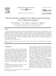
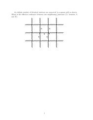
Fig. 12. Model of the Bi 4+<br />
M<br />
antisite defect. ODMR measurements show that the<br />
hole is delocalized to an O 2− neighbor of Bi 3+ . There it is stabilized by lattice<br />
distortion, caused by the decreased attraction between O − <strong>and</strong> Bi 3+ . Because of<br />
the <strong>in</strong>itial equivalence of the tetrahedrally arranged oxygen ions, the system can be<br />
called a bound small hole polaron. The process of optical absorption is <strong>in</strong>dicated<br />
by the dashed l<strong>in</strong>e: the hole is transferred under Franck-Condon conditions from its<br />
<strong>in</strong>itial O − site to a neighbor<strong>in</strong>g O 2− -ion. Because of the equivalence of the three<br />
f<strong>in</strong>al O 2− -ions, a tunnel<strong>in</strong>g of the excited hole among them is expected, lead<strong>in</strong>g to<br />
two optical absorption b<strong>and</strong>s of nearly equal <strong>in</strong>tensities <strong>and</strong> widths [11]. The dashed<br />
hole transition can alternatively be viewed as a transition of an electron from the<br />
O 2− -ions, be<strong>in</strong>g part of the valence b<strong>and</strong>, to O − . This expla<strong>in</strong>s the transitions 2 <strong>and</strong><br />
3 <strong>in</strong> Fig. 13.<br />
The ODMR [151, 149], performed with the MCD signals ’1 - 3’, could be<br />
attributed to one unpaired sp<strong>in</strong> (S =1/2) with a strong hyperf<strong>in</strong>e coupl<strong>in</strong>g<br />
to the nuclear sp<strong>in</strong> (9/2) of the 100% abundant 209 Bi. All evidence led to<br />
the assignment of the MCD signals to an antisite defect [156] Bi 4+ or - <strong>in</strong><br />
M<br />
more detail - Bi 3+<br />
M<br />
’dressed’ by a hole, delocalized on one of the four tetrahedral<br />
oxygen neighbors. Although the observed symmetry of the defect was<br />
essentially isotropic, trigonal distortion was not excluded [157]. As concluded<br />
from the ODMR-MCD studies, all b<strong>and</strong>s ’1 - 3’ <strong>in</strong> Fig. 6 have the same Bi 4+<br />
M<br />
<strong>in</strong>itial state. B<strong>and</strong>s ’4 <strong>and</strong> 5’, <strong>in</strong> contrast, have to be assigned to different paramagnetic<br />
species [146] show<strong>in</strong>g a very broad ODMR signal for microwaves at<br />
35 GHz [153]. The magnetic <strong>and</strong> optical properties of Al 4+<br />
Si<br />
[150] <strong>and</strong> Ga 4+<br />
Si<br />
[153] were also established for the first time by ODMR.<br />
The transitions lead<strong>in</strong>g to the observed optical properties of all these defects<br />
are shown <strong>in</strong> Fig. 13. In the bleached state only the charge state Bi 3+<br />
M<br />
is<br />
present. The CD b<strong>and</strong> (’0’) associated with the absorption shoulder reflects<br />
the spectral dependence of the photoionization of an electron from Bi 3+<br />
M<br />
to<br />
the conduction b<strong>and</strong>; its onset around 2.4 eV at 77 K or lower <strong>and</strong> around