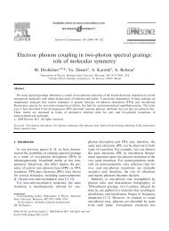
Practical Uses and Applications of Electro-Optic Modulators
Practical Uses and Applications of Electro-Optic Modulators
Practical Uses and Applications of Electro-Optic Modulators

You also want an ePaper? Increase the reach of your titles
YUMPU automatically turns print PDFs into web optimized ePapers that Google loves.
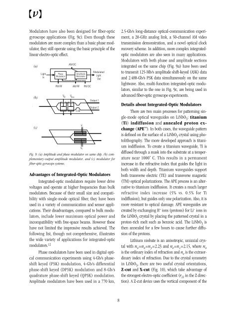
<strong>Modulators</strong> have also been designed for fiber-optic<br />
gyroscope applications (Fig. 9c). Even though these<br />
modulators are more complex than a basic phase modulator,<br />
they still operate using the basic principle <strong>of</strong> the<br />
linear electro-optic effect.<br />
(a)<br />
(b)<br />
(c)<br />
Light<br />
In<br />
Phase<br />
Modulator<br />
PM RF<br />
VRF<br />
AM DC<br />
VBias<br />
Amplitude<br />
Modulator<br />
AM RF<br />
Fig. 9: (a) Amplitude <strong>and</strong> phase modulator on same chip, (b) complementary-output<br />
amplitude modulator, <strong>and</strong> (c) modulator for<br />
fiber-optic gyroscope systems.<br />
Advantages <strong>of</strong> Integrated-<strong>Optic</strong> <strong>Modulators</strong><br />
Integrated-optic modulators require lower drive<br />
voltages <strong>and</strong> operate at higher frequencies than bulk<br />
modulators. Because <strong>of</strong> their small size <strong>and</strong> compatibility<br />
with single-mode optical fiber, they have been<br />
used in a variety <strong>of</strong> communication <strong>and</strong> sensor applications.<br />
Their disadvantages, compared to bulk modulators,<br />
include lower maximum optical power <strong>and</strong><br />
incompatibility with free-space beams. However these<br />
have not limited the impressive results achieved. The<br />
following list, though not comprehensive, illustrates<br />
the wide variety <strong>of</strong> applications for integrated-optic<br />
modulators. 12<br />
Phase modulators have been used in digital optical<br />
communication experiments using 4-Gb/s phaseshift<br />
keyed (PSK) modulation, 4-Gb/s differential<br />
phase-shift keyed (DPSK) modulation <strong>and</strong> 8-Gb/s<br />
quadrature phase-shift keyed (QPSK) modulation.<br />
Amplitude modulators have been used in a 770 km,<br />
3 db<br />
V 1<br />
V2<br />
PM DC<br />
Modulated <br />
Light <br />
Out<br />
Output 1<br />
Output 2<br />
2.5-Gb/s long-distance optical-communication experiment,<br />
a 20-GHz analog link, a 50-channel AM video<br />
transmission demonstration, <strong>and</strong> a novel optical clock<br />
recovery scheme. In addition, more complex integratedoptic<br />
modulators are also seen in many applications.<br />
<strong>Modulators</strong> with both phase <strong>and</strong> amplitude sections<br />
integrated on the same chip (Fig. 9a) have been used<br />
to transmit 125-Mb/s amplitude shift-keyed (ASK) data<br />
<strong>and</strong> 2.488-Gb/s PSK data simultaneously on the same<br />
lightwave. Also, multi-function integrated-optic modulators,<br />
similar to the one in Fig. 9c, are being used in<br />
advanced fiber-optic gyroscope experiments.<br />
Details about Integrated-<strong>Optic</strong> <strong>Modulators</strong><br />
There are two main processes for patterning single-mode<br />
optical waveguides on LiNbO 3 : titanium<br />
(Ti) indiffusion <strong>and</strong> annealed proton exchange<br />
(APE ). In both cases, the waveguide pattern<br />
is defined on the surface <strong>of</strong> a LiNbO 3 crystal using photolithography.<br />
The more developed approach is titanium<br />
indiffusion. To create a titanium waveguide, Ti is<br />
diffused through a mask into the substrate at a temperature<br />
near 1000˚ C. This results in a permanent<br />
increase in the refractive index that guides the light in<br />
both width <strong>and</strong> depth. Titanium waveguides support<br />
both transverse electric (TE) <strong>and</strong> transverse magnetic<br />
(TM) optical polarizations. The APE process is an alternative<br />
to titanium indiffusion. It creates a much larger<br />
refractive index increase (5% vs. 0.5% for Ti<br />
indiffusion), but guides only one polarization. Also, it is<br />
more resistant to optical damage. APE waveguides are<br />
created by exchanging H + ions (protons) for Li + ions in<br />
the LiNbO 3 crystal by placing the patterned crystal in a<br />
proton-rich melt such as benzoic acid. The LiNbO 3 is<br />
then annealed for a few hours to cause further diffusion<br />
<strong>of</strong> the protons.<br />
Lithium niobate is an anisotropic, uniaxial crystal<br />
with n o =n x =n y =2.23 <strong>and</strong> n e =n z =2.15, where n o<br />
is the ordinary index <strong>of</strong> refraction <strong>and</strong> n e is the extraordinary<br />
index <strong>of</strong> refraction. Due to the crystal symmetry<br />
in LiNbO 3 , there are two useful crystal orientations,<br />
Z-cut <strong>and</strong> X-cut (Fig. 10), which take advantage <strong>of</strong><br />
the strongest electro-optic coefficient (r 33 in the Z direction).<br />
A Z-cut device uses the vertical component <strong>of</strong> the<br />
8