B32656S - Semikron
B32656S - Semikron
B32656S - Semikron

Create successful ePaper yourself
Turn your PDF publications into a flip-book with our unique Google optimized e-Paper software.
Film Capacitors<br />
Metallized Polypropylene Film Capacitors (MKP)<br />
Series/Type:<br />
<strong>B32656S</strong><br />
Date: February 2010<br />
© EPCOS AG 2010. Reproduction, publication and dissemination of this publication, enclosures hereto and the<br />
information contained therein without EPCOS' prior express consent is prohibited.
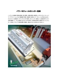
Metallized polypropylene film capacitors (MKP)<br />
Snubber (wound)<br />
<strong>B32656S</strong><br />
Typical applications<br />
IGBT<br />
Snubbering<br />
Climatic<br />
Max. operating temperature: 110 °C<br />
Climatic category (IEC 60068-1): 55/100/56<br />
Construction<br />
Dielectric: polypropylene (PP)<br />
Wound capacitor technology with internal<br />
series connection<br />
Plastic case (UL 94 V-0)<br />
Epoxy resin sealing (UL 94 V-0)<br />
Features<br />
High pulse strength and high contact reliability<br />
Very low inductance<br />
Terminals<br />
Strap terminals, tinned copper or brass (max. torque 10 Nm)<br />
Marking<br />
Manufacturer's logo, ordering code, style (MKP)<br />
rated capacitance (coded), cap. tolerance (code letter),<br />
rated DC voltage, date of manufacture (coded)<br />
Delivery mode<br />
Bulk (untaped)<br />
Dimensional drawings<br />
T1 (code no. 561) T2 (code no. 562)<br />
Please read Cautions and warnings and<br />
Important notes at the end of this document.<br />
Page 2 of 31
<strong>B32656S</strong><br />
Snubber (wound)<br />
Dimensional drawings (continued)<br />
T3 (code no. 563) T4 (code no. 564)<br />
T5 (code no. 565) T6 (code no. 566)<br />
Please read Cautions and warnings and<br />
Important notes at the end of this document.<br />
Page 3 of 31
<strong>B32656S</strong><br />
Snubber (wound)<br />
T7 (code no. 577)<br />
Please read Cautions and warnings and<br />
Important notes at the end of this document.<br />
Page 4 of 31
<strong>B32656S</strong><br />
Snubber (wound)<br />
Overview of available types<br />
Type <strong>B32656S</strong><br />
V R (V DC) 850 1000 1250 1600 2000<br />
V RMS (V AC) 450 480 500 750 800<br />
C R (nF)<br />
47<br />
68<br />
100<br />
120<br />
150<br />
220<br />
270<br />
330<br />
390<br />
470<br />
560<br />
680<br />
820<br />
1000<br />
1200<br />
1500<br />
1800<br />
2200<br />
2700<br />
3300<br />
Please read Cautions and warnings and<br />
Important notes at the end of this document.<br />
Page 5 of 31
<strong>B32656S</strong><br />
Snubber (wound)<br />
Electrical specifications, ordering codes and packing units<br />
V R<br />
V DC<br />
V RMS<br />
f≤1kHz<br />
V AC<br />
C R<br />
nF<br />
Max. dimensions<br />
w × h × l<br />
mm<br />
I RMS<br />
100 kHz<br />
A<br />
ESR<br />
100 kHz<br />
mΩ<br />
MOQ = Minimum Order Quantity, consisting of 4 packing units.<br />
Further E series and intermediate capacitance values on request.<br />
Composition of ordering code<br />
+ = Capacitance tolerance code:<br />
K = ±10%<br />
J = ±5%<br />
Ordering code<br />
(composition see<br />
below)<br />
Terminal<br />
pcs./<br />
MOQ<br />
850 450 220 12.0 × 22.5 × 42.0 5 10.0 <strong>B32656S</strong>8224+563 T3 224<br />
220 12.0 × 22.5 × 42.0 5 10.0 <strong>B32656S</strong>8224+564 T4 384<br />
270 12.0 × 22.5 × 42.0 6 9.0 <strong>B32656S</strong>8274+563 T3 224<br />
270 12.0 × 22.5 × 42.0 6 9.0 <strong>B32656S</strong>8274+564 T4 384<br />
330 12.0 × 22.5 × 42.0 6 9.0 <strong>B32656S</strong>8334+563 T3 224<br />
330 12.0 × 22.5 × 42.0 6 9.0 <strong>B32656S</strong>8334+564 T4 384<br />
390 12.0 × 22.5 × 42.0 7 8.0 <strong>B32656S</strong>8394+563 T3 224<br />
390 12.0 × 22.5 × 42.0 7 8.0 <strong>B32656S</strong>8394+564 T4 384<br />
470 12.0 × 22.5 × 42.0 8 8.0 <strong>B32656S</strong>8474+563 T3 224<br />
470 12.0 × 22.5 × 42.0 8 8.0 <strong>B32656S</strong>8474+564 T4 384<br />
560 14.0 × 25.0 × 42.0 8 7.0 <strong>B32656S</strong>8564+563 T3 168<br />
560 14.0 × 25.0 × 42.0 8 7.0 <strong>B32656S</strong>8564+564 T4 288<br />
560 14.0 × 25.0 × 42.0 8 7.0 <strong>B32656S</strong>8564+565 T5 288<br />
680 16.0 × 28.5 × 42.0 9 6.0 <strong>B32656S</strong>8684+561 T1 192<br />
680 16.0 × 28.5 × 42.0 9 6.0 <strong>B32656S</strong>8684+562 T2 192<br />
680 16.0 × 28.5 × 42.0 9 6.0 <strong>B32656S</strong>8684+563 T3 144<br />
680 16.0 × 28.5 × 42.0 9 6.0 <strong>B32656S</strong>8684+564 T4 192<br />
680 16.0 × 28.5 × 42.0 9 6.0 <strong>B32656S</strong>8684+565 T5 192<br />
680 16.0 × 28.5 × 42.0 9 6.0 <strong>B32656S</strong>8684+566 T6 192<br />
680 16.0 × 28.5 × 42.0 9 6.0 <strong>B32656S</strong>8684+577 T7 180<br />
820 16.0 × 28.5 × 42.0 10 6.0 <strong>B32656S</strong>8824+561 T1 192<br />
820 16.0 × 28.5 × 42.0 10 6.0 <strong>B32656S</strong>8824+562 T2 192<br />
820 16.0 × 28.5 × 42.0 10 6.0 <strong>B32656S</strong>8824+563 T3 144<br />
820 16.0 × 28.5 × 42.0 10 6.0 <strong>B32656S</strong>8824+564 T4 192<br />
820 16.0 × 28.5 × 42.0 10 6.0 <strong>B32656S</strong>8824+565 T5 192<br />
820 16.0 × 28.5 × 42.0 10 6.0 <strong>B32656S</strong>8824+566 T6 192<br />
820 16.0 × 28.5 × 42.0 10 6.0 <strong>B32656S</strong>8824+577 T7 180<br />
Please read Cautions and warnings and<br />
Important notes at the end of this document.<br />
Page 6 of 31
<strong>B32656S</strong><br />
Snubber (wound)<br />
Electrical specifications, ordering codes and packing units<br />
V R<br />
V DC<br />
V RMS<br />
f≤1kHz<br />
V AC<br />
C R<br />
nF<br />
Max. dimensions<br />
w × h × l<br />
mm<br />
I RMS<br />
100 kHz<br />
A<br />
ESR<br />
100 kHz<br />
mΩ<br />
MOQ = Minimum Order Quantity, consisting of 4 packing units.<br />
Further E series and intermediate capacitance values on request.<br />
Composition of ordering code<br />
+ = Capacitance tolerance code:<br />
K = ±10%<br />
J = ±5%<br />
Ordering code<br />
(composition see<br />
below)<br />
Terminal<br />
pcs./<br />
MOQ<br />
850 450 1000 18.0 × 32.5 × 42.0 11 6.0 <strong>B32656S</strong>8105+561 T1 168<br />
1000 18.0 × 32.5 × 42.0 11 6.0 <strong>B32656S</strong>8105+562 T2 168<br />
1000 18.0 × 32.5 × 42.0 11 6.0 <strong>B32656S</strong>8105+563 T3 144<br />
1000 18.0 × 32.5 × 42.0 11 6.0 <strong>B32656S</strong>8105+564 T4 128<br />
1000 18.0 × 32.5 × 42.0 11 6.0 <strong>B32656S</strong>8105+565 T5 128<br />
1000 18.0 × 32.5 × 42.0 11 6.0 <strong>B32656S</strong>8105+566 T6 168<br />
1000 18.0 × 32.5 × 42.0 11 6.0 <strong>B32656S</strong>8105+577 T7 156<br />
1200 18.0 × 32.5 × 42.0 11 5.0 <strong>B32656S</strong>8125+561 T1 168<br />
1200 18.0 × 32.5 × 42.0 11 5.0 <strong>B32656S</strong>8125+562 T2 168<br />
1200 18.0 × 32.5 × 42.0 11 5.0 <strong>B32656S</strong>8125+563 T3 144<br />
1200 18.0 × 32.5 × 42.0 11 5.0 <strong>B32656S</strong>8125+564 T4 128<br />
1200 18.0 × 32.5 × 42.0 11 5.0 <strong>B32656S</strong>8125+565 T5 128<br />
1200 18.0 × 32.5 × 42.0 11 5.0 <strong>B32656S</strong>8125+566 T6 168<br />
1200 18.0 × 32.5 × 42.0 11 5.0 <strong>B32656S</strong>8125+577 T7 156<br />
1500 31.0 × 26.5 × 43.6 13 5.0 <strong>B32656S</strong>8155+561 T1 128<br />
1500 31.0 × 26.5 × 43.6 13 5.0 <strong>B32656S</strong>8155+562 T2 128<br />
1500 31.0 × 26.5 × 43.6 13 5.0 <strong>B32656S</strong>8155+563 T3 72<br />
1500 31.0 × 26.5 × 43.6 13 5.0 <strong>B32656S</strong>8155+566 T6 128<br />
1500 31.0 × 26.5 × 43.6 13 5.0 <strong>B32656S</strong>8155+577 T7 84<br />
1800 28.0 × 37.0 × 42.0 15 4.5 <strong>B32656S</strong>8185+561 T1 108<br />
1800 28.0 × 37.0 × 42.0 15 4.5 <strong>B32656S</strong>8185+562 T2 108<br />
1800 28.0 × 37.0 × 42.0 15 4.5 <strong>B32656S</strong>8185+563 T3 96<br />
1800 28.0 × 37.0 × 42.0 15 4.5 <strong>B32656S</strong>8185+566 T6 108<br />
1800 28.0 × 37.0 × 42.0 15 4.5 <strong>B32656S</strong>8185+577 T7 96<br />
2200 30.0 × 45.0 × 42.0 17 3.5 <strong>B32656S</strong>8225+561 T1 48<br />
2200 30.0 × 45.0 × 42.0 17 3.5 <strong>B32656S</strong>8225+562 T2 48<br />
2200 30.0 × 45.0 × 42.0 17 3.5 <strong>B32656S</strong>8225+563 T3 96<br />
2200 30.0 × 45.0 × 42.0 17 3.5 <strong>B32656S</strong>8225+566 T6 48<br />
2200 30.0 × 45.0 × 42.0 17 3.5 <strong>B32656S</strong>8225+577 T7 96<br />
Please read Cautions and warnings and<br />
Important notes at the end of this document.<br />
Page 7 of 31
<strong>B32656S</strong><br />
Snubber (wound)<br />
Electrical specifications, ordering codes and packing units<br />
V R<br />
V DC<br />
V RMS<br />
f≤1kHz<br />
V AC<br />
C R<br />
nF<br />
Max. dimensions<br />
w × h × l<br />
mm<br />
I RMS<br />
100 kHz<br />
A<br />
ESR<br />
100 kHz<br />
mΩ<br />
MOQ = Minimum Order Quantity, consisting of 4 packing units.<br />
Further E series and intermediate capacitance values on request.<br />
Composition of ordering code<br />
+ = Capacitance tolerance code:<br />
K = ±10%<br />
J = ±5%<br />
Ordering code<br />
(composition see<br />
below)<br />
Terminal<br />
pcs./<br />
MOQ<br />
1000 480 680 16.0 × 28.5 × 42.0 10 6.0 <strong>B32656S</strong>0684+561 T1 192<br />
680 16.0 × 28.5 × 42.0 10 6.0 <strong>B32656S</strong>0684+562 T2 192<br />
680 16.0 × 28.5 × 42.0 10 6.0 <strong>B32656S</strong>0684+563 T3 144<br />
680 16.0 × 28.5 × 42.0 10 6.0 <strong>B32656S</strong>0684+564 T4 192<br />
680 16.0 × 28.5 × 42.0 10 6.0 <strong>B32656S</strong>0684+565 T5 192<br />
680 16.0 × 28.5 × 42.0 10 6.0 <strong>B32656S</strong>0684+566 T6 192<br />
680 16.0 × 28.5 × 42.0 10 6.0 <strong>B32656S</strong>0684+577 T7 180<br />
820 18.0 × 32.5 × 42.0 11 6.0 <strong>B32656S</strong>0824+561 T1 168<br />
820 18.0 × 32.5 × 42.0 11 6.0 <strong>B32656S</strong>0824+562 T2 168<br />
820 18.0 × 32.5 × 42.0 11 6.0 <strong>B32656S</strong>0824+563 T3 144<br />
820 18.0 × 32.5 × 42.0 11 6.0 <strong>B32656S</strong>0824+564 T4 128<br />
820 18.0 × 32.5 × 42.0 11 6.0 <strong>B32656S</strong>0824+565 T5 128<br />
820 18.0 × 32.5 × 42.0 11 6.0 <strong>B32656S</strong>0824+566 T6 168<br />
820 18.0 × 32.5 × 42.0 11 6.0 <strong>B32656S</strong>0824+577 T7 156<br />
1000 20.0 × 39.5 × 42.0 12 6.0 <strong>B32656S</strong>0105+561 T1 96<br />
1000 20.0 × 39.5 × 42.0 12 6.0 <strong>B32656S</strong>0105+562 T2 96<br />
1000 20.0 × 39.5 × 42.0 12 6.0 <strong>B32656S</strong>0105+563 T3 104<br />
1000 20.0 × 39.5 × 42.0 12 6.0 <strong>B32656S</strong>0105+564 T4 96<br />
1000 20.0 × 39.5 × 42.0 12 6.0 <strong>B32656S</strong>0105+565 T5 96<br />
1000 20.0 × 39.5 × 42.0 12 6.0 <strong>B32656S</strong>0105+566 T6 96<br />
1000 20.0 × 39.5 × 42.0 12 6.0 <strong>B32656S</strong>0105+577 T7 144<br />
1200 20.0 × 39.5 × 42.0 13 5.0 <strong>B32656S</strong>0125+561 T1 96<br />
1200 20.0 × 39.5 × 42.0 13 5.0 <strong>B32656S</strong>0125+562 T2 96<br />
1200 20.0 × 39.5 × 42.0 13 5.0 <strong>B32656S</strong>0125+563 T3 104<br />
1200 20.0 × 39.5 × 42.0 13 5.0 <strong>B32656S</strong>0125+564 T4 96<br />
1200 20.0 × 39.5 × 42.0 13 5.0 <strong>B32656S</strong>0125+565 T5 96<br />
1200 20.0 × 39.5 × 42.0 13 5.0 <strong>B32656S</strong>0125+566 T6 96<br />
1200 20.0 × 39.5 × 42.0 13 5.0 <strong>B32656S</strong>0125+577 T7 144<br />
Please read Cautions and warnings and<br />
Important notes at the end of this document.<br />
Page 9 of 31
<strong>B32656S</strong><br />
Snubber (wound)<br />
Electrical specifications, ordering codes and packing units<br />
V R<br />
V DC<br />
V RMS<br />
f≤1kHz<br />
V AC<br />
C R<br />
nF<br />
Max. dimensions<br />
w × h × l<br />
mm<br />
I RMS<br />
100 kHz<br />
A<br />
ESR<br />
100 kHz<br />
mΩ<br />
MOQ = Minimum Order Quantity, consisting of 4 packing units.<br />
Further E series and intermediate capacitance values on request.<br />
Composition of ordering code<br />
+ = Capacitance tolerance code:<br />
K = ±10%<br />
J = ±5%<br />
Ordering code<br />
(composition see<br />
below)<br />
Terminal<br />
pcs./<br />
MOQ<br />
1000 480 1500 30.0 × 45.0 × 42.0 15 5.0 <strong>B32656S</strong>0155+561 T1 48<br />
1500 30.0 × 45.0 × 42.0 15 5.0 <strong>B32656S</strong>0155+562 T2 48<br />
1500 30.0 × 45.0 × 42.0 15 5.0 <strong>B32656S</strong>0155+563 T3 96<br />
1500 30.0 × 45.0 × 42.0 15 5.0 <strong>B32656S</strong>0155+566 T6 48<br />
1500 30.0 × 45.0 × 42.0 15 5.0 <strong>B32656S</strong>0155+577 T7 96<br />
1800 30.0 × 45.0 × 42.0 16 4.5 <strong>B32656S</strong>0185+561 T1 48<br />
1800 30.0 × 45.0 × 42.0 16 4.5 <strong>B32656S</strong>0185+562 T2 48<br />
1800 30.0 × 45.0 × 42.0 16 4.5 <strong>B32656S</strong>0185+563 T3 96<br />
1800 30.0 × 45.0 × 42.0 16 4.5 <strong>B32656S</strong>0185+566 T6 48<br />
1800 30.0 × 45.0 × 42.0 16 4.5 <strong>B32656S</strong>0185+577 T7 96<br />
2200 30.0 × 45.0 × 42.0 19 3.5 <strong>B32656S</strong>0225+561 T1 48<br />
2200 30.0 × 45.0 × 42.0 19 3.5 <strong>B32656S</strong>0225+562 T2 48<br />
2200 30.0 × 45.0 × 42.0 19 3.5 <strong>B32656S</strong>0225+563 T3 96<br />
2200 30.0 × 45.0 × 42.0 19 3.5 <strong>B32656S</strong>0225+566 T6 48<br />
2200 30.0 × 45.0 × 42.0 19 3.5 <strong>B32656S</strong>0225+577 T7 96<br />
2700 33.0 × 48.0 × 43.0 23 2.5 <strong>B32656S</strong>0275+561 T1 84<br />
2700 33.0 × 48.0 × 43.0 23 2.5 <strong>B32656S</strong>0275+562 T2 84<br />
2700 33.0 × 48.0 × 43.0 23 2.5 <strong>B32656S</strong>0275+563 T3 64<br />
2700 33.0 × 48.0 × 43.0 23 2.5 <strong>B32656S</strong>0275+566 T6 84<br />
2700 33.0 × 48.0 × 43.0 23 2.5 <strong>B32656S</strong>0275+577 T7 84<br />
1250 500 120 12.0 × 22.5 × 42.0 5 15.0 <strong>B32656S</strong>7124+563 T3 224<br />
120 12.0 × 22.5 × 42.0 5 15.0 <strong>B32656S</strong>7124+564 T4 384<br />
150 12.0 × 22.5 × 42.0 6 15.0 <strong>B32656S</strong>7154+563 T3 224<br />
150 12.0 × 22.5 × 42.0 6 15.0 <strong>B32656S</strong>7154+564 T4 384<br />
220 14.0 × 25.0 × 42.0 8 10.0 <strong>B32656S</strong>7224+563 T3 168<br />
220 14.0 × 25.0 × 42.0 8 10.0 <strong>B32656S</strong>7224+564 T4 288<br />
220 14.0 × 25.0 × 42.0 8 10.0 <strong>B32656S</strong>7224+565 T5 288<br />
270 14.0 × 25.0 × 42.0 8 9.0 <strong>B32656S</strong>7274+563 T3 168<br />
270 14.0 × 25.0 × 42.0 8 9.0 <strong>B32656S</strong>7274+564 T4 288<br />
270 14.0 × 25.0 × 42.0 8 9.0 <strong>B32656S</strong>7274+565 T5 288<br />
Please read Cautions and warnings and<br />
Important notes at the end of this document.<br />
Page 10 of 31
<strong>B32656S</strong><br />
Snubber (wound)<br />
Electrical specifications, ordering codes and packing units<br />
V R<br />
V DC<br />
V RMS<br />
f≤1kHz<br />
V AC<br />
C R<br />
nF<br />
Max. dimensions<br />
w × h × l<br />
mm<br />
I RMS<br />
100 kHz<br />
A<br />
ESR<br />
100 kHz<br />
mΩ<br />
MOQ = Minimum Order Quantity, consisting of 4 packing units.<br />
Further E series and intermediate capacitance values on request.<br />
Composition of ordering code<br />
+ = Capacitance tolerance code:<br />
K = ±10%<br />
J = ±5%<br />
Ordering code<br />
(composition see<br />
below)<br />
Terminal<br />
pcs./<br />
MOQ<br />
1250 500 330 16.0 × 28.5 × 42.0 8 9.0 <strong>B32656S</strong>7334+561 T1 192<br />
330 16.0 × 28.5 × 42.0 8 9.0 <strong>B32656S</strong>7334+562 T2 192<br />
330 16.0 × 28.5 × 42.0 8 9.0 <strong>B32656S</strong>7334+563 T3 144<br />
330 16.0 × 28.5 × 42.0 8 9.0 <strong>B32656S</strong>7334+564 T4 192<br />
330 16.0 × 28.5 × 42.0 8 9.0 <strong>B32656S</strong>7334+565 T5 192<br />
330 16.0 × 28.5 × 42.0 8 9.0 <strong>B32656S</strong>7334+566 T6 192<br />
330 16.0 × 28.5 × 42.0 8 9.0 <strong>B32656S</strong>7334+577 T7 180<br />
390 18.0 × 32.5 × 42.0 9 8.0 <strong>B32656S</strong>7394+561 T1 168<br />
390 18.0 × 32.5 × 42.0 9 8.0 <strong>B32656S</strong>7394+562 T2 168<br />
390 18.0 × 32.5 × 42.0 9 8.0 <strong>B32656S</strong>7394+563 T3 144<br />
390 18.0 × 32.5 × 42.0 9 8.0 <strong>B32656S</strong>7394+564 T4 128<br />
390 18.0 × 32.5 × 42.0 9 8.0 <strong>B32656S</strong>7394+565 T5 128<br />
390 18.0 × 32.5 × 42.0 9 8.0 <strong>B32656S</strong>7394+566 T6 168<br />
390 18.0 × 32.5 × 42.0 9 8.0 <strong>B32656S</strong>7394+577 T7 156<br />
470 18.0 × 32.5 × 42.0 9 8.0 <strong>B32656S</strong>7474+561 T1 168<br />
470 18.0 × 32.5 × 42.0 9 8.0 <strong>B32656S</strong>7474+562 T2 168<br />
470 18.0 × 32.5 × 42.0 9 8.0 <strong>B32656S</strong>7474+563 T3 144<br />
470 18.0 × 32.5 × 42.0 9 8.0 <strong>B32656S</strong>7474+564 T4 128<br />
470 18.0 × 32.5 × 42.0 9 8.0 <strong>B32656S</strong>7474+565 T5 128<br />
470 18.0 × 32.5 × 42.0 9 8.0 <strong>B32656S</strong>7474+566 T6 168<br />
470 18.0 × 32.5 × 42.0 9 8.0 <strong>B32656S</strong>7474+577 T7 156<br />
560 20.0 × 39.5 × 42.0 10 7.0 <strong>B32656S</strong>7564+561 T1 96<br />
560 20.0 × 39.5 × 42.0 10 7.0 <strong>B32656S</strong>7564+562 T2 96<br />
560 20.0 × 39.5 × 42.0 10 7.0 <strong>B32656S</strong>7564+563 T3 104<br />
560 20.0 × 39.5 × 42.0 10 7.0 <strong>B32656S</strong>7564+564 T4 96<br />
560 20.0 × 39.5 × 42.0 10 7.0 <strong>B32656S</strong>7564+565 T5 96<br />
560 20.0 × 39.5 × 42.0 10 7.0 <strong>B32656S</strong>7564+566 T6 96<br />
560 20.0 × 39.5 × 42.0 10 7.0 <strong>B32656S</strong>7564+577 T7 144<br />
Please read Cautions and warnings and<br />
Important notes at the end of this document.<br />
Page 11 of 31
<strong>B32656S</strong><br />
Snubber (wound)<br />
Electrical specifications, ordering codes and packing units<br />
V R<br />
V DC<br />
V RMS<br />
f≤1kHz<br />
V AC<br />
C R<br />
nF<br />
Max. dimensions<br />
w × h × l<br />
mm<br />
I RMS<br />
100 kHz<br />
A<br />
ESR<br />
100 kHz<br />
mΩ<br />
MOQ = Minimum Order Quantity, consisting of 4 packing units.<br />
Further E series and intermediate capacitance values on request.<br />
Composition of ordering code<br />
+ = Capacitance tolerance code:<br />
K = ±10%<br />
J = ±5%<br />
Ordering code<br />
(composition see<br />
below)<br />
Terminal<br />
pcs./<br />
MOQ<br />
1250 500 680 20.0 × 39.5 × 42.0 12 6.0 <strong>B32656S</strong>7684+561 T1 96<br />
680 20.0 × 39.5 × 42.0 12 6.0 <strong>B32656S</strong>7684+562 T2 96<br />
680 20.0 × 39.5 × 42.0 12 6.0 <strong>B32656S</strong>7684+563 T3 104<br />
680 20.0 × 39.5 × 42.0 12 6.0 <strong>B32656S</strong>7684+564 T4 96<br />
680 20.0 × 39.5 × 42.0 12 6.0 <strong>B32656S</strong>7684+565 T5 96<br />
680 20.0 × 39.5 × 42.0 12 6.0 <strong>B32656S</strong>7684+566 T6 96<br />
680 20.0 × 39.5 × 42.0 12 6.0 <strong>B32656S</strong>7684+577 T7 144<br />
820 28.0 × 37.0 × 42.0 13 6.0 <strong>B32656S</strong>7824+561 T1 108<br />
820 28.0 × 37.0 × 42.0 13 6.0 <strong>B32656S</strong>7824+562 T2 108<br />
820 28.0 × 37.0 × 42.0 13 6.0 <strong>B32656S</strong>7824+563 T3 72<br />
820 28.0 × 37.0 × 42.0 13 6.0 <strong>B32656S</strong>7824+566 T6 108<br />
820 28.0 × 37.0 × 42.0 13 6.0 <strong>B32656S</strong>7824+577 T7 96<br />
1000 28.0 × 37.0 × 42.0 15 6.0 <strong>B32656S</strong>7105+561 T1 108<br />
1000 28.0 × 37.0 × 42.0 15 6.0 <strong>B32656S</strong>7105+562 T2 108<br />
1000 28.0 × 37.0 × 42.0 15 6.0 <strong>B32656S</strong>7105+563 T3 72<br />
1000 28.0 × 37.0 × 42.0 15 6.0 <strong>B32656S</strong>7105+566 T6 108<br />
1000 28.0 × 37.0 × 42.0 15 6.0 <strong>B32656S</strong>7105+577 T7 96<br />
1200 30.0 × 45.0 × 42.0 16 5.0 <strong>B32656S</strong>7125+561 T1 48<br />
1200 30.0 × 45.0 × 42.0 16 5.0 <strong>B32656S</strong>7125+562 T2 48<br />
1200 30.0 × 45.0 × 42.0 16 5.0 <strong>B32656S</strong>7125+563 T3 72<br />
1200 30.0 × 45.0 × 42.0 16 5.0 <strong>B32656S</strong>7125+566 T6 48<br />
1200 30.0 × 45.0 × 42.0 16 5.0 <strong>B32656S</strong>7125+577 T7 96<br />
1500 30.0 × 45.0 × 42.0 18 4.0 <strong>B32656S</strong>7155+561 T1 48<br />
1500 30.0 × 45.0 × 42.0 18 4.0 <strong>B32656S</strong>7155+562 T2 48<br />
1500 30.0 × 45.0 × 42.0 18 4.0 <strong>B32656S</strong>7155+563 T3 72<br />
1500 30.0 × 45.0 × 42.0 18 4.0 <strong>B32656S</strong>7155+566 T6 48<br />
1500 30.0 × 45.0 × 42.0 18 4.0 <strong>B32656S</strong>7155+577 T7 96<br />
1800 33.0 × 48.0 × 43.0 22 3.0 <strong>B32656S</strong>7185+561 T1 84<br />
1800 33.0 × 48.0 × 43.0 22 3.0 <strong>B32656S</strong>7185+562 T2 84<br />
1800 33.0 × 48.0 × 43.0 22 3.0 <strong>B32656S</strong>7185+563 T3 64<br />
1800 33.0 × 48.0 × 43.0 22 3.0 <strong>B32656S</strong>7185+566 T6 84<br />
1800 33.0 × 48.0 × 43.0 22 3.0 <strong>B32656S</strong>7185+577 T7 84<br />
Please read Cautions and warnings and<br />
Important notes at the end of this document.<br />
Page 12 of 31
<strong>B32656S</strong><br />
Snubber (wound)<br />
Electrical specifications, ordering codes and packing units<br />
V R<br />
V DC<br />
V RMS<br />
f≤1kHz<br />
V AC<br />
C R<br />
nF<br />
Max. dimensions<br />
w × h × l<br />
mm<br />
I RMS<br />
100 kHz<br />
A<br />
ESR<br />
100 kHz<br />
mΩ<br />
MOQ = Minimum Order Quantity, consisting of 4 packing units.<br />
Further E series and intermediate capacitance values on request.<br />
Composition of ordering code<br />
+ = Capacitance tolerance code:<br />
K = ±10%<br />
J = ±5%<br />
Ordering code<br />
(composition see<br />
below)<br />
Terminal<br />
pcs./<br />
MOQ<br />
1600 750 68 12.0 × 22.5 × 42.0 5 25.0 <strong>B32656S</strong>1683+563 T3 224<br />
68 12.0 × 22.5 × 42.0 5 25.0 <strong>B32656S</strong>1683+564 T4 384<br />
100 12.0 × 22.5 × 42.0 6 20.0 <strong>B32656S</strong>1104+563 T3 224<br />
100 12.0 × 22.5 × 42.0 6 20.0 <strong>B32656S</strong>1104+564 T4 384<br />
120 14.0 × 25.0 × 42.0 6 15.0 <strong>B32656S</strong>1124+563 T3 168<br />
120 14.0 × 25.0 × 42.0 6 15.0 <strong>B32656S</strong>1124+564 T4 288<br />
120 14.0 × 25.0 × 42.0 6 15.0 <strong>B32656S</strong>1124+565 T5 288<br />
150 14.0 × 25.0 × 42.0 7 15.0 <strong>B32656S</strong>1154+563 T3 168<br />
150 14.0 × 25.0 × 42.0 7 15.0 <strong>B32656S</strong>1154+564 T4 288<br />
150 14.0 × 25.0 × 42.0 7 15.0 <strong>B32656S</strong>1154+565 T5 288<br />
220 16.0 × 28.5 × 42.0 9 10.0 <strong>B32656S</strong>1224+561 T1 192<br />
220 16.0 × 28.5 × 42.0 9 10.0 <strong>B32656S</strong>1224+562 T2 192<br />
220 16.0 × 28.5 × 42.0 9 10.0 <strong>B32656S</strong>1224+563 T3 144<br />
220 16.0 × 28.5 × 42.0 9 10.0 <strong>B32656S</strong>1224+564 T4 192<br />
220 16.0 × 28.5 × 42.0 9 10.0 <strong>B32656S</strong>1224+565 T5 192<br />
220 16.0 × 28.5 × 42.0 9 10.0 <strong>B32656S</strong>1224+566 T6 192<br />
220 16.0 × 28.5 × 42.0 9 10.0 <strong>B32656S</strong>1224+577 T7 180<br />
270 18.0 × 32.5 × 42.0 10 9.0 <strong>B32656S</strong>1274+561 T1 168<br />
270 18.0 × 32.5 × 42.0 10 9.0 <strong>B32656S</strong>1274+562 T2 168<br />
270 18.0 × 32.5 × 42.0 10 9.0 <strong>B32656S</strong>1274+563 T3 144<br />
270 18.0 × 32.5 × 42.0 10 9.0 <strong>B32656S</strong>1274+564 T4 128<br />
270 18.0 × 32.5 × 42.0 10 9.0 <strong>B32656S</strong>1274+565 T5 128<br />
270 18.0 × 32.5 × 42.0 10 9.0 <strong>B32656S</strong>1274+566 T6 168<br />
270 18.0 × 32.5 × 42.0 10 9.0 <strong>B32656S</strong>1274+577 T7 156<br />
330 20.0 × 39.5 × 42.0 12 9.0 <strong>B32656S</strong>1334+561 T1 96<br />
330 20.0 × 39.5 × 42.0 12 9.0 <strong>B32656S</strong>1334+562 T2 96<br />
330 20.0 × 39.5 × 42.0 12 9.0 <strong>B32656S</strong>1334+563 T3 104<br />
330 20.0 × 39.5 × 42.0 12 9.0 <strong>B32656S</strong>1334+564 T4 96<br />
330 20.0 × 39.5 × 42.0 12 9.0 <strong>B32656S</strong>1334+565 T5 96<br />
330 20.0 × 39.5 × 42.0 12 9.0 <strong>B32656S</strong>1334+566 T6 96<br />
330 20.0 × 39.5 × 42.0 12 9.0 <strong>B32656S</strong>1334+577 T7 144<br />
Please read Cautions and warnings and<br />
Important notes at the end of this document.<br />
Page 13 of 31
<strong>B32656S</strong><br />
Snubber (wound)<br />
Electrical specifications, ordering codes and packing units<br />
V R<br />
V DC<br />
V RMS<br />
f≤1kHz<br />
V AC<br />
C R<br />
nF<br />
Max. dimensions<br />
w × h × l<br />
mm<br />
I RMS<br />
100 kHz<br />
A<br />
ESR<br />
100 kHz<br />
mΩ<br />
MOQ = Minimum Order Quantity, consisting of 4 packing units.<br />
Further E series and intermediate capacitance values on request.<br />
Composition of ordering code<br />
+ = Capacitance tolerance code:<br />
K = ±10%<br />
J = ±5%<br />
Ordering code<br />
(composition see<br />
below)<br />
Terminal<br />
pcs./<br />
MOQ<br />
1600 750 390 28.0 × 37.0 × 42.0 13 8.0 <strong>B32656S</strong>1394+561 T1 108<br />
390 28.0 × 37.0 × 42.0 13 8.0 <strong>B32656S</strong>1394+562 T2 108<br />
390 28.0 × 37.0 × 42.0 13 8.0 <strong>B32656S</strong>1394+563 T3 72<br />
390 28.0 × 37.0 × 42.0 13 8.0 <strong>B32656S</strong>1394+566 T6 108<br />
390 28.0 × 37.0 × 42.0 13 8.0 <strong>B32656S</strong>1394+577 T7 96<br />
470 28.0 × 37.0 × 42.0 14 8.0 <strong>B32656S</strong>1474+561 T1 108<br />
470 28.0 × 37.0 × 42.0 14 8.0 <strong>B32656S</strong>1474+562 T2 108<br />
470 28.0 × 37.0 × 42.0 14 8.0 <strong>B32656S</strong>1474+563 T3 72<br />
470 28.0 × 37.0 × 42.0 14 8.0 <strong>B32656S</strong>1474+566 T6 108<br />
470 28.0 × 37.0 × 42.0 14 8.0 <strong>B32656S</strong>1474+577 T7 96<br />
560 30.0 × 45.0 × 42.0 15 7.0 <strong>B32656S</strong>1564+561 T1 48<br />
560 30.0 × 45.0 × 42.0 15 7.0 <strong>B32656S</strong>1564+562 T2 48<br />
560 30.0 × 45.0 × 42.0 15 7.0 <strong>B32656S</strong>1564+563 T3 72<br />
560 30.0 × 45.0 × 42.0 15 7.0 <strong>B32656S</strong>1564+566 T6 48<br />
560 30.0 × 45.0 × 42.0 15 7.0 <strong>B32656S</strong>1564+577 T7 96<br />
680 30.0 × 45.0 × 42.0 17 6.0 <strong>B32656S</strong>1684+561 T1 48<br />
680 30.0 × 45.0 × 42.0 17 6.0 <strong>B32656S</strong>1684+562 T2 48<br />
680 30.0 × 45.0 × 42.0 17 6.0 <strong>B32656S</strong>1684+563 T3 72<br />
680 30.0 × 45.0 × 42.0 17 6.0 <strong>B32656S</strong>1684+566 T6 48<br />
680 30.0 × 45.0 × 42.0 17 6.0 <strong>B32656S</strong>1684+577 T7 96<br />
820 33.0 × 48.0 × 43.0 20 4.5 <strong>B32656S</strong>1824+561 T1 84<br />
820 33.0 × 48.0 × 43.0 20 4.5 <strong>B32656S</strong>1824+562 T2 84<br />
820 33.0 × 48.0 × 43.0 20 4.5 <strong>B32656S</strong>1824+563 T3 64<br />
820 33.0 × 48.0 × 43.0 20 4.5 <strong>B32656S</strong>1824+566 T6 84<br />
820 33.0 × 48.0 × 43.0 20 4.5 <strong>B32656S</strong>1824+577 T7 84<br />
Please read Cautions and warnings and<br />
Important notes at the end of this document.<br />
Page 14 of 31
<strong>B32656S</strong><br />
Snubber (wound)<br />
Electrical specifications, ordering codes and packing units<br />
V R<br />
V DC<br />
V RMS<br />
f≤1kHz<br />
V AC<br />
C R<br />
nF<br />
Max. dimensions<br />
w × h × l<br />
mm<br />
I RMS<br />
100 kHz<br />
A<br />
ESR<br />
100 kHz<br />
mΩ<br />
MOQ = Minimum Order Quantity, consisting of 4 packing units.<br />
Further E series and intermediate capacitance values on request.<br />
Composition of ordering code<br />
+ = Capacitance tolerance code:<br />
K = ±10%<br />
J = ±5%<br />
Ordering code<br />
(composition see<br />
below)<br />
Terminal<br />
pcs./<br />
MOQ<br />
2000 800 47 12.0 × 22.5 × 42.0 5 35.0 <strong>B32656S</strong>2473+563 T3 224<br />
47 12.0 × 22.5 × 42.0 5 35.0 <strong>B32656S</strong>2473+564 T4 384<br />
68 14.0 × 25.0 × 42.0 6 25.0 <strong>B32656S</strong>2683+563 T3 192<br />
68 14.0 × 25.0 × 42.0 6 25.0 <strong>B32656S</strong>2683+564 T4 288<br />
68 14.0 × 25.0 × 42.0 6 25.0 <strong>B32656S</strong>2683+565 T5 288<br />
100 14.0 × 25.0 × 42.0 7 20.0 <strong>B32656S</strong>2104+563 T3 192<br />
100 14.0 × 25.0 × 42.0 7 20.0 <strong>B32656S</strong>2104+564 T4 288<br />
100 14.0 × 25.0 × 42.0 7 20.0 <strong>B32656S</strong>2104+565 T5 288<br />
120 16.0 × 28.5 × 42.0 7 15.0 <strong>B32656S</strong>2124+561 T1 192<br />
120 16.0 × 28.5 × 42.0 7 15.0 <strong>B32656S</strong>2124+562 T2 192<br />
120 16.0 × 28.5 × 42.0 7 15.0 <strong>B32656S</strong>2124+563 T3 144<br />
120 16.0 × 28.5 × 42.0 7 15.0 <strong>B32656S</strong>2124+564 T4 192<br />
120 16.0 × 28.5 × 42.0 7 15.0 <strong>B32656S</strong>2124+565 T5 192<br />
120 16.0 × 28.5 × 42.0 7 15.0 <strong>B32656S</strong>2124+566 T6 192<br />
120 16.0 × 28.5 × 42.0 7 15.0 <strong>B32656S</strong>2124+577 T7 180<br />
150 18.0 × 32.5 × 42.0 9 15.0 <strong>B32656S</strong>2154+561 T1 168<br />
150 18.0 × 32.5 × 42.0 9 15.0 <strong>B32656S</strong>2154+562 T2 168<br />
150 18.0 × 32.5 × 42.0 9 15.0 <strong>B32656S</strong>2154+563 T3 160<br />
150 18.0 × 32.5 × 42.0 9 15.0 <strong>B32656S</strong>2154+564 T4 192<br />
150 18.0 × 32.5 × 42.0 9 15.0 <strong>B32656S</strong>2154+565 T5 192<br />
150 18.0 × 32.5 × 42.0 9 15.0 <strong>B32656S</strong>2154+566 T6 168<br />
150 18.0 × 32.5 × 42.0 9 15.0 <strong>B32656S</strong>2154+577 T7 156<br />
220 20.0 × 39.5 × 42.0 12 10.0 <strong>B32656S</strong>2224+561 T1 96<br />
220 20.0 × 39.5 × 42.0 12 10.0 <strong>B32656S</strong>2224+562 T2 96<br />
220 20.0 × 39.5 × 42.0 12 10.0 <strong>B32656S</strong>2224+563 T3 104<br />
220 20.0 × 39.5 × 42.0 12 10.0 <strong>B32656S</strong>2224+564 T4 96<br />
220 20.0 × 39.5 × 42.0 12 10.0 <strong>B32656S</strong>2224+565 T5 96<br />
220 20.0 × 39.5 × 42.0 12 10.0 <strong>B32656S</strong>2224+566 T6 96<br />
220 20.0 × 39.5 × 42.0 12 10.0 <strong>B32656S</strong>2224+577 T7 144<br />
Please read Cautions and warnings and<br />
Important notes at the end of this document.<br />
Page 15 of 31
<strong>B32656S</strong><br />
Snubber (wound)<br />
Electrical specifications, ordering codes and packing units<br />
V R<br />
V DC<br />
V RMS<br />
f≤1kHz<br />
V AC<br />
C R<br />
nF<br />
Max. dimensions<br />
w × h × l<br />
mm<br />
I RMS<br />
100 kHz<br />
A<br />
ESR<br />
100 kHz<br />
mΩ<br />
MOQ = Minimum Order Quantity, consisting of 4 packing units.<br />
Further E series and intermediate capacitance values on request.<br />
Composition of ordering code<br />
+ = Capacitance tolerance code:<br />
K = ±10%<br />
J = ±5%<br />
Ordering code<br />
(composition see<br />
below)<br />
Terminal<br />
pcs./<br />
MOQ<br />
2000 800 270 28.0 × 37.0 × 42.0 13 9.0 <strong>B32656S</strong>2274+561 T1 108<br />
270 28.0 × 37.0 × 42.0 13 9.0 <strong>B32656S</strong>2274+562 T2 108<br />
270 28.0 × 37.0 × 42.0 13 9.0 <strong>B32656S</strong>2274+563 T3 72<br />
270 28.0 × 37.0 × 42.0 13 9.0 <strong>B32656S</strong>2274+566 T6 108<br />
270 28.0 × 37.0 × 42.0 13 9.0 <strong>B32656S</strong>2274+577 T7 96<br />
330 28.0 × 37.0 × 42.0 14 9.0 <strong>B32656S</strong>2334+561 T1 108<br />
330 28.0 × 37.0 × 42.0 14 9.0 <strong>B32656S</strong>2334+562 T2 108<br />
330 28.0 × 37.0 × 42.0 14 9.0 <strong>B32656S</strong>2334+563 T3 72<br />
330 28.0 × 37.0 × 42.0 14 9.0 <strong>B32656S</strong>2334+566 T6 108<br />
330 28.0 × 37.0 × 42.0 14 9.0 <strong>B32656S</strong>2334+577 T7 96<br />
390 30.0 × 45.0 × 42.0 15 8.0 <strong>B32656S</strong>2394+561 T1 48<br />
390 30.0 × 45.0 × 42.0 15 8.0 <strong>B32656S</strong>2394+562 T2 48<br />
390 30.0 × 45.0 × 42.0 15 8.0 <strong>B32656S</strong>2394+563 T3 72<br />
390 30.0 × 45.0 × 42.0 15 8.0 <strong>B32656S</strong>2394+566 T6 48<br />
390 30.0 × 45.0 × 42.0 15 8.0 <strong>B32656S</strong>2394+577 T7 96<br />
470 30.0 × 45.0 × 42.0 17 8.0 <strong>B32656S</strong>2474+561 T1 48<br />
470 30.0 × 45.0 × 42.0 17 8.0 <strong>B32656S</strong>2474+562 T2 48<br />
470 30.0 × 45.0 × 42.0 17 8.0 <strong>B32656S</strong>2474+563 T3 72<br />
470 30.0 × 45.0 × 42.0 17 8.0 <strong>B32656S</strong>2474+566 T6 48<br />
470 30.0 × 45.0 × 42.0 17 8.0 <strong>B32656S</strong>2474+577 T7 96<br />
560 33.0 × 48.0 × 43.0 20 6.5 <strong>B32656S</strong>2564+561 T1 84<br />
560 33.0 × 48.0 × 43.0 20 6.5 <strong>B32656S</strong>2564+562 T2 84<br />
560 33.0 × 48.0 × 43.0 20 6.5 <strong>B32656S</strong>2564+563 T3 64<br />
560 33.0 × 48.0 × 43.0 20 6.5 <strong>B32656S</strong>2564+566 T6 84<br />
560 33.0 × 48.0 × 43.0 20 6.5 <strong>B32656S</strong>2564+577 T7 84<br />
Please read Cautions and warnings and<br />
Important notes at the end of this document.<br />
Page 16 of 31
<strong>B32656S</strong><br />
Snubber (wound)<br />
Technical data<br />
Operating temperature range Max. operating temperature T op,max +110 °C<br />
Upper category temperature T max +100 °C<br />
Lower category temperature T min 55 °C<br />
Rated temperature T R +85 °C<br />
Dissipation factor tan δ (in 10 -3 ) at C R ≤0.1 µF 0.1 µF1 µF<br />
at 20 °C 1 kHz 0.5 0.5<br />
(upper limit values) 10 kHz 0.8 1.5<br />
100 kHz 5.0 <br />
Insulation resistance R ins C R ≤ 0.33 µF C R > 0.33 µF<br />
or time constant τ = C R R ins 100 GΩ 30000 s<br />
at 20 °C, rel. humidity ≤ 65%<br />
(minimum as-delivered values)<br />
DC test voltage<br />
1.6 V R , 2 s<br />
Category voltage V C T A (°C) DC voltage derating AC voltage derating<br />
(continuous operation with V DC T A ≤ 85 V C = V R V C,RMS = V RMS<br />
or V AC at f ≤ 1 kHz) 85 4 upper limit value<br />
Insulation resistance R ins<br />
or time constant τ = C R R ins<br />
< 1500 MΩ (C R ≤0.33 µF)<br />
< 500 s (C R >0.33 µF)<br />
Please read Cautions and warnings and<br />
Important notes at the end of this document.<br />
Page 17 of 31
<strong>B32656S</strong><br />
Snubber (wound)<br />
Pulse handling capability<br />
"dV/dt" represents the maximum permissible voltage change per unit of time for non-sinusoidal<br />
voltages, expressed in V/µs.<br />
"k 0 " represents the maximum permissible pulse characteristic of the waveform applied to the<br />
capacitor, expressed in V 2 /µs.<br />
Note:<br />
The values of dV/dt and k 0 provided below must not be exceeded in order to avoid damaging the<br />
capacitor.<br />
dV/dt and k 0 values<br />
V R (V DC) V RMS (V AC) dV/dt in V/µs k 0 in V 2 /µs<br />
850 450 400 680 000<br />
1000 480 450 900 000<br />
1250 500 500 1 250 000<br />
1600 750 600 1 920 000<br />
2000 800 700 2 800 000<br />
Impedance Z versus frequency f<br />
(typical values)<br />
Please read Cautions and warnings and<br />
Important notes at the end of this document.<br />
Page 18 of 31
<strong>B32656S</strong><br />
Snubber (wound)<br />
Permissible AC voltage V RMS versus frequency f (for sinusoidal waveforms, T A ≤90 °C)<br />
For T A >90 °C, please refer to "General technical information", section 3.2.3.<br />
850 V DC/450 V AC 1000 V DC/480 V AC<br />
1250 V DC/500 V AC 1600 V DC/750 V AC<br />
Please read Cautions and warnings and<br />
Important notes at the end of this document.<br />
Page 19 of 31
<strong>B32656S</strong><br />
Snubber (wound)<br />
Permissible AC voltage V RMS versus frequency f (for sinusoidal waveforms, T A ≤90 °C)<br />
For T A >90 °C, please refer to "General technical information", section 3.2.3.<br />
2000 V DC/800 V AC<br />
Please read Cautions and warnings and<br />
Important notes at the end of this document.<br />
Page 20 of 31
<strong>B32656S</strong><br />
Snubber (wound)<br />
Mounting guidelines<br />
1 Soldering<br />
1.1 Solderability of leads<br />
The solderability of terminal leads is tested to IEC 60068-2-20, test Ta, method 1.<br />
Before a solderability test is carried out, terminals are subjected to accelerated ageing (to<br />
IEC 60068-2-2, test Ba: 4 h exposure to dry heat at 155 °C). Since the ageing temperature is far<br />
higher than the upper category temperature of the capacitors, the terminal wires should be cut off<br />
from the capacitor before the ageing procedure to prevent the solderability being impaired by the<br />
products of any capacitor decomposition that might occur.<br />
Solder bath temperature 235 ±5 °C<br />
Soldering time<br />
Immersion depth<br />
Evaluation criteria:<br />
Visual inspection<br />
2.0 ±0.5 s<br />
1.2 Resistance to soldering heat<br />
2.0 +0/0.5 mm from capacitor body or seating plane<br />
Wetting of wire surface by new solder ≥90%, free-flowing solder<br />
Resistance to soldering heat is tested to IEC 60068-2-20, test Tb, method 1A.<br />
Conditions:<br />
Series Solder bath temperature Soldering time<br />
MKT<br />
MFP<br />
MKP<br />
boxed (except 2.5 × 6.5 × 7.2 mm)<br />
coated<br />
uncoated (lead spacing > 10 mm)<br />
(lead spacing > 7.5 mm)<br />
260 ±5 °C 10 ±1 s<br />
MKT boxed (case 2.5 × 6.5 × 7.2 mm) 5 ±1 s<br />
MKP<br />
MKT<br />
(lead spacing ≤ 7.5 mm)<br />
uncoated (lead spacing ≤ 10 mm)<br />
insulated (B32559)<br />
< 4 s<br />
recommended soldering<br />
profile for MKT uncoated<br />
(lead spacing ≤ 10 mm) and<br />
insulated (B32559)<br />
Please read Cautions and warnings and<br />
Important notes at the end of this document.<br />
Page 21 of 31
<strong>B32656S</strong><br />
Snubber (wound)<br />
Immersion depth<br />
Shield<br />
Evaluation criteria:<br />
Visual inspection<br />
∆C/C 0<br />
tan δ<br />
2.0 +0/0.5 mm from capacitor body or seating plane<br />
Heat-absorbing board, (1.5 ±0.5) mm thick, between capacitor<br />
body and liquid solder<br />
No visible damage<br />
2% for MKT/MKP/MFP<br />
5% for EMI suppression capacitors<br />
As specified in sectional specification<br />
Please read Cautions and warnings and<br />
Important notes at the end of this document.<br />
Page 22 of 31
<strong>B32656S</strong><br />
Snubber (wound)<br />
1.3 General notes on soldering<br />
Permissible heat exposure loads on film capacitors are primarily characterized by the upper category<br />
temperature T max . Long exposure to temperatures above this type-related temperature limit<br />
can lead to changes in the plastic dielectric and thus change irreversibly a capacitor's electrical<br />
characteristics. For short exposures (as in practical soldering processes) the heat load (and thus<br />
the possible effects on a capacitor) will also depend on other factors like:<br />
Pre-heating temperature and time<br />
Forced cooling immediately after soldering<br />
Terminal characteristics:<br />
diameter, length, thermal resistance, special configurations (e.g. crimping)<br />
Height of capacitor above solder bath<br />
Shadowing by neighboring components<br />
Additional heating due to heat dissipation by neighboring components<br />
Use of solder-resist coatings<br />
The overheating associated with some of these factors can usually be reduced by suitable countermeasures.<br />
For example, if a pre-heating step cannot be avoided, an additional or reinforced<br />
cooling process may possibly have to be included.<br />
EPCOS recommends the following conditions:<br />
Pre-heating with a maximum temperature of 110 °C<br />
Temperature inside the capacitor should not exceed the following limits:<br />
MKP/MFP 110 °C<br />
MKT 160 °C<br />
When SMD components are used together with leaded ones, the leaded film capacitors should<br />
not pass into the SMD adhesive curing oven. The leaded components should be assembled after<br />
the SMD curing step.<br />
Leaded film capacitors are not suitable for reflow soldering.<br />
Uncoated capacitors<br />
For uncoated MKT capacitors with lead spacings ≤10 mm (B32560/B32561) the following measures<br />
are recommended:<br />
pre-heating to not more than 110 °C in the preheater phase<br />
rapid cooling after soldering<br />
Please read Cautions and warnings and<br />
Important notes at the end of this document.<br />
Page 23 of 31
<strong>B32656S</strong><br />
Snubber (wound)<br />
2 Cleaning<br />
To determine whether the following solvents, often used to remove flux residues and other substances,<br />
are suitable for the capacitors described, refer to the table below:<br />
Type<br />
MKT<br />
(uncoated)<br />
MKT, MKP, MFP<br />
(coated/boxed)<br />
Ethanol,<br />
isopropanol,<br />
n-propanol<br />
n-propanol-water<br />
mixtures,<br />
water with surface<br />
tension-reducing<br />
tensides (neutral)<br />
Solvent from<br />
table A (see<br />
next page)<br />
Solvent from<br />
table B (see<br />
next page)<br />
Suitable Unsuitable In part suitable Unsuitable<br />
Suitable<br />
Suitable<br />
Table A<br />
Manufacturers' designations for trifluoro-trichloro-ethane-based cleaning solvents (selection)<br />
Even when suitable solvents are used, a reversible change of the electrical characteristics may<br />
occur in uncoated capacitors immediately after they are washed. Thus it is always recommended<br />
to dry the components (e.g. 4 h at 70 °C) before they are subjected to subsequent electrical testing.<br />
Trifluoro-trichloroethane<br />
Mixtures of trifluoro-trichloro-ethane with ethanol and<br />
isopropanol<br />
Manufacturer<br />
Freon TF Freon TE 35; Freon TP 35; Freon TES Du Pont<br />
Frigen 113 TR Frigen 113 TR-E; Frigen 113 TR-P; Frigen TR-E 35 Hoechst<br />
Arklone P Arklone A; Arklone L; Arklone K ICI<br />
Kaltron 113 MDR Kaltron 113 MDA; Kaltron 113 MDI; Kaltron 113 MDI 35 Kali-Chemie<br />
Flugene 113 Flugene 113 E; Flugene 113 IPA Rhone-Progil<br />
Table B (worldwide banned substances)<br />
Manufacturers' designations for unsuitable cleaning solvents (selection)<br />
Mixtures of chlorinated hydrocarbons and ketones with fluorated hydrocarbons<br />
Freon TMC; Freon TA; Freon TC<br />
Arklone E<br />
Kaltron 113 MDD; Kaltron 113 MDK<br />
Flugene 113 CM<br />
Manufacturer<br />
Du Pont<br />
ICI<br />
Kali-Chemie<br />
Rhone-Progil<br />
Please read Cautions and warnings and<br />
Important notes at the end of this document.<br />
Page 24 of 31
<strong>B32656S</strong><br />
Snubber (wound)<br />
3 Embedding of capacitors in finished assemblies<br />
In many applications, finished circuit assemblies are embedded in plastic resins. In this case,<br />
both chemical and thermal influences of the embedding ("potting") and curing processes must be<br />
taken into account.<br />
Our experience has shown that the following potting materials can be recommended: non-flexible<br />
epoxy resins with acid-anhydride hardeners; chemically inert, non-conducting fillers; maximum<br />
curing temperature of 100 °C.<br />
Caution:<br />
Consult us first if you wish to embed uncoated types!<br />
Please read Cautions and warnings and<br />
Important notes at the end of this document.<br />
Page 25 of 31
<strong>B32656S</strong><br />
Snubber (wound)<br />
Cautions and warnings<br />
Do not exceed the upper category temperature (UCT).<br />
Do not apply any mechanical stress to the capacitor terminals.<br />
Avoid any compressive, tensile or flexural stress.<br />
Do not move the capacitor after it has been soldered to the PC board.<br />
Do not pick up the PC board by the soldered capacitor.<br />
Do not place the capacitor on a PC board whose PTH hole spacing differs from the specified<br />
lead spacing.<br />
Do not exceed the specified time or temperature limits during soldering.<br />
Avoid external energy inputs, such as fire or electricity.<br />
Avoid overload of the capacitors.<br />
The table below summarizes the safety instructions that must always be observed. A detailed description<br />
can be found in the relevant sections of the chapters "General technical information" and<br />
"Mounting guidelines".<br />
Topic Safety information Reference chapter<br />
"General technical<br />
information"<br />
Storage conditions<br />
Flammability<br />
Resistance to<br />
vibration<br />
Make sure that capacitors are stored within the<br />
specified range of time, temperature and humidity<br />
conditions.<br />
Avoid external energy, such as fire or electricity<br />
(passive flammability), avoid overload of the<br />
capacitors (active flammability) and consider the<br />
flammability of materials.<br />
4.5<br />
"Storage conditions"<br />
5.3<br />
"Flammability"<br />
Do not exceed the tested ability to withstand 5.2<br />
vibration. The capacitors are tested to<br />
"Resistance to vibration"<br />
IEC 60068-2-6.<br />
EPCOS offers film capacitors specially designed<br />
for operation under more severe vibration regimes<br />
such as those found in automotive applications.<br />
Consult our catalog "Film Capacitors for<br />
Automotive Electronics".<br />
Please read Cautions and warnings and<br />
Important notes at the end of this document.<br />
Page 26 of 31
<strong>B32656S</strong><br />
Snubber (wound)<br />
Topic Safety information Reference chapter<br />
"Mounting guidelines"<br />
Soldering<br />
Cleaning<br />
Embedding of<br />
capacitors in<br />
finished assemblies<br />
Do not exceed the specified time or temperature<br />
limits during soldering.<br />
1 "Soldering"<br />
Use only suitable solvents for cleaning capacitors. 2 "Cleaning"<br />
When embedding finished circuit assemblies in<br />
plastic resins, chemical and thermal influences<br />
must be taken into account.<br />
Caution: Consult us first, if you also wish to<br />
embed other uncoated component types!<br />
3 "Embedding of<br />
capacitors in finished<br />
assemblies"<br />
Please read Cautions and warnings and<br />
Important notes at the end of this document.<br />
Page 27 of 31
<strong>B32656S</strong><br />
Snubber (wound)<br />
Symbols and terms<br />
Symbol English German<br />
α Heat transfer coefficient Wärmeübergangszahl<br />
α C Temperature coefficient of capacitance Temperaturkoeffizient der Kapazität<br />
A Capacitor surface area Kondensatoroberfläche<br />
β C Humidity coefficient of capacitance Feuchtekoeffizient der Kapazität<br />
C Capacitance Kapazität<br />
C R Rated capacitance Nennkapazität<br />
∆C Absolute capacitance change Absolute Kapazitätsänderung<br />
∆C/C<br />
∆C/C R<br />
Relative capacitance change (relative<br />
deviation of actual value)<br />
Capacitance tolerance (relative deviation<br />
from rated capacitance)<br />
dt Time differential Differentielle Zeit<br />
∆t Time interval Zeitintervall<br />
∆T<br />
Absolute temperature change<br />
(self-heating)<br />
Relative Kapazitätsänderung (relative<br />
Abweichung vom Ist-Wert)<br />
Kapazitätstoleranz (relative Abweichung<br />
vom Nennwert)<br />
Absolute Temperaturänderung<br />
(Selbsterwärmung)<br />
∆tan δ Absolute change of dissipation factor Absolute Änderung des Verlustfaktors<br />
∆V Absolute voltage change Absolute Spannungsänderung<br />
dV/dt<br />
Time differential of voltage function (rate<br />
of voltage rise)<br />
Differentielle Spannungsänderung<br />
(Spannungsflankensteilheit)<br />
∆V/∆t Voltage change per time interval Spannungsänderung pro Zeitintervall<br />
E Activation energy for diffusion Aktivierungsenergie zur Diffusion<br />
ESL Self-inductance Eigeninduktivität<br />
ESR Equivalent series resistance Ersatz-Serienwiderstand<br />
f Frequency Frequenz<br />
f 1<br />
f 2<br />
Frequency limit for reducing permissible<br />
AC voltage due to thermal limits<br />
Frequency limit for reducing permissible<br />
AC voltage due to current limit<br />
Grenzfrequenz für thermisch bedingte<br />
Reduzierung der zulässigen<br />
Wechselspannung<br />
Grenzfrequenz für strombedingte<br />
Reduzierung der zulässigen<br />
Wechselspannung<br />
f r Resonant frequency Resonanzfrequenz<br />
F D Thermal acceleration factor for diffusion Therm. Beschleunigungsfaktor zur<br />
Diffusion<br />
F T Derating factor Deratingfaktor<br />
i Current (peak) Stromspitze<br />
I C<br />
Category current (max. continuous<br />
current)<br />
Kategoriestrom (max. Dauerstrom)<br />
Please read Cautions and warnings and<br />
Important notes at the end of this document.<br />
Page 28 of 31
<strong>B32656S</strong><br />
Snubber (wound)<br />
Symbol English German<br />
I RMS<br />
(Sinusoidal) alternating current,<br />
root-mean-square value<br />
(Sinusförmiger) Wechselstrom<br />
i z Capacitance drift Inkonstanz der Kapazität<br />
k 0 Pulse characteristic Impulskennwert<br />
L S Series inductance Serieninduktivität<br />
λ Failure rate Ausfallrate<br />
λ 0<br />
Constant failure rate during useful<br />
service life<br />
Konstante Ausfallrate in der<br />
Nutzungsphase<br />
λ test Failure rate, determined by tests Experimentell ermittelte Ausfallrate<br />
P diss Dissipated power Abgegebene Verlustleistung<br />
P gen Generated power Erzeugte Verlustleistung<br />
Q Heat energy Wärmeenergie<br />
ρ Density of water vapor in air Dichte von Wasserdampf in Luft<br />
R Universal molar constant for gases Allg. Molarkonstante für Gas<br />
R Ohmic resistance of discharge circuit Ohmscher Widerstand des<br />
Entladekreises<br />
R i Internal resistance Innenwiderstand<br />
R ins Insulation resistance Isolationswiderstand<br />
R P Parallel resistance Parallelwiderstand<br />
R S Series resistance Serienwiderstand<br />
S severity (humidity test) Schärfegrad (Feuchtetest)<br />
t Time Zeit<br />
T Temperature Temperatur<br />
τ Time constant Zeitkonstante<br />
tan δ Dissipation factor Verlustfaktor<br />
tan δ D<br />
Dielectric component of dissipation<br />
factor<br />
Dielektrischer Anteil des Verlustfaktors<br />
tan δ P Parallel component of dissipation factor Parallelanteil des Verlfustfaktors<br />
tan δ S Series component of dissipation factor Serienanteil des Verlustfaktors<br />
T A Ambient temperature Umgebungstemperatur<br />
T max Upper category temperature Obere Kategorietemperatur<br />
T min Lower category temperature Untere Kategorietemperatur<br />
t OL<br />
Operating life at operating temperature<br />
and voltage<br />
T op Operating temperature Beriebstemperatur<br />
T R Rated temperature Nenntemperatur<br />
Betriebszeit bei Betriebstemperatur und<br />
-spannung<br />
T ref Reference temperature Referenztemperatur<br />
t SL Reference service life Referenz-Lebensdauer<br />
V AC AC voltage Wechselspannung<br />
Please read Cautions and warnings and<br />
Important notes at the end of this document.<br />
Page 29 of 31
<strong>B32656S</strong><br />
Snubber (wound)<br />
Symbol English German<br />
V C Category voltage Kategoriespannung<br />
V C,RMS Category AC voltage (Sinusförmige)<br />
Kategorie-Wechselspannung<br />
V CD Corona-discharge onset voltage Teilentlade-Einsatzspannung<br />
V ch Charging voltage Ladespannung<br />
V DC DC voltage Gleichspannung<br />
V FB Fly-back capacitor voltage Spannung (Flyback)<br />
V i Input voltage Eingangsspannung<br />
V o Output voltage Ausgangssspannung<br />
V op Operating voltage Betriebsspannung<br />
V p Peak pulse voltage Impuls-Spitzenspannung<br />
V pp Peak-to-peak voltage Impedance Spannungshub<br />
V R Rated voltage Nennspannung<br />
R Amplitude of rated AC voltage Amplitude der Nenn-Wechselspannung<br />
V RMS<br />
(Sinusoidal) alternating voltage,<br />
root-mean-square value<br />
(Sinusförmige) Wechselspannung<br />
V SC S-correction voltage Spannung bei Anwendung "S-correction"<br />
V sn Snubber capacitor voltage Spannung bei Anwendung<br />
"Beschaltung"<br />
Z Impedance Scheinwiderstand<br />
Lead spacing<br />
Rastermaß<br />
Please read Cautions and warnings and<br />
Important notes at the end of this document.<br />
Page 30 of 31
Important notes<br />
The following applies to all products named in this publication:<br />
1. Some parts of this publication contain statements about the suitability of our products for<br />
certain areas of application. These statements are based on our knowledge of typical requirements<br />
that are often placed on our products in the areas of application concerned. We<br />
nevertheless expressly point out that such statements cannot be regarded as binding<br />
statements about the suitability of our products for a particular customer application.<br />
As a rule, EPCOS is either unfamiliar with individual customer applications or less familiar<br />
with them than the customers themselves. For these reasons, it is always ultimately incumbent<br />
on the customer to check and decide whether an EPCOS product with the properties described<br />
in the product specification is suitable for use in a particular customer application.<br />
2. We also point out that in individual cases, a malfunction of electronic components or<br />
failure before the end of their usual service life cannot be completely ruled out in the<br />
current state of the art, even if they are operated as specified. In customer applications<br />
requiring a very high level of operational safety and especially in customer applications in<br />
which the malfunction or failure of an electronic component could endanger human life or<br />
health (e.g. in accident prevention or lifesaving systems), it must therefore be ensured by<br />
means of suitable design of the customer application or other action taken by the customer<br />
(e.g. installation of protective circuitry or redundancy) that no injury or damage is sustained by<br />
third parties in the event of malfunction or failure of an electronic component.<br />
3. The warnings, cautions and product-specific notes must be observed.<br />
4. In order to satisfy certain technical requirements, some of the products described in this<br />
publication may contain substances subject to restrictions in certain jurisdictions (e.g.<br />
because they are classed as hazardous). Useful information on this will be found in our Material<br />
Data Sheets on the Internet (www.epcos.com/material). Should you have any more detailed<br />
questions, please contact our sales offices.<br />
5. We constantly strive to improve our products. Consequently, the products described in this<br />
publication may change from time to time. The same is true of the corresponding product<br />
specifications. Please check therefore to what extent product descriptions and specifications<br />
contained in this publication are still applicable before or when you place an order. We also<br />
reserve the right to discontinue production and delivery of products. Consequently, we<br />
cannot guarantee that all products named in this publication will always be available. The<br />
aforementioned does not apply in the case of individual agreements deviating from the foregoing<br />
for customer-specific products.<br />
6. Unless otherwise agreed in individual contracts, all orders are subject to the current version<br />
of the "General Terms of Delivery for Products and Services in the Electrical Industry"<br />
published by the German Electrical and Electronics Industry Association<br />
(ZVEI).<br />
7. The trade names EPCOS, BAOKE, Alu-X, CeraDiode, CSMP, CSSP, CTVS, DeltaCap,<br />
DigiSiMic, DSSP, MiniBlue, MiniCell, MKK, MLSC, MotorCap, PCC, PhaseCap, PhaseCube,<br />
PhaseMod, PhiCap, SIFERRIT, SIFI, SIKOREL, SilverCap, SIMDAD, SiMic, SIMID,<br />
SineFormer, SIOV, SIP5D, SIP5K, ThermoFuse, WindCap are trademarks registered or<br />
pending in Europe and in other countries. Further information will be found on the Internet at<br />
www.epcos.com/trademarks.<br />
Page 31 of 31