SEMIKRON leading manufacturer of igbt, diode thyristor power ...
SEMIKRON leading manufacturer of igbt, diode thyristor power ...
SEMIKRON leading manufacturer of igbt, diode thyristor power ...

Create successful ePaper yourself
Turn your PDF publications into a flip-book with our unique Google optimized e-Paper software.
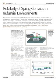
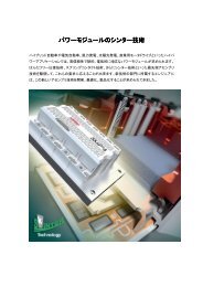
Low temperature sinter technology<br />
Die attachment for automotive <strong>power</strong> electronic applications<br />
C. Göbl 1 , P. Beckedahl 2, H. Braml 3<br />
1: <strong>SEMIKRON</strong> Elektronik Gmbh & CoKG C. Göbl, Sigmundstr. 200 D- 90441 Nürnberg<br />
2: <strong>SEMIKRON</strong> International Gmbh P. Beckedahl , Sigmundstr. 200 D- 90441 Nürnberg<br />
3: <strong>SEMIKRON</strong> Elektronik Gmbh & CoKG H. Braml, Sigmundstr. 200 D-90441 Nürnberg<br />
Abstract:<br />
New fields <strong>of</strong> high <strong>power</strong> inverter systems such like<br />
hybrid cars, hybrid trucks, and <strong>of</strong>f road vehicles<br />
require new ways <strong>of</strong> <strong>power</strong> electronics integration<br />
and packaging. The stringent requirements in size<br />
and weight, reliability, durability, ambient<br />
temperature, and environment are driving the<br />
operation temperatures <strong>of</strong> <strong>power</strong> electronics beyond<br />
the limits <strong>of</strong> today’s industrial applications. In<br />
industrial <strong>power</strong> modules solder and bond wires are<br />
still the standard joining technologies <strong>of</strong> <strong>power</strong> dies.<br />
These technologies are reaching their reliability limits<br />
if die temperatures are pushed above 125°C.<br />
In this paper the authors will discuss how the<br />
environmental conditions <strong>of</strong> automotive applications<br />
drive silicon <strong>power</strong> device selection and packaging<br />
technologies. Extreme cooling conditions and ultra<br />
high <strong>power</strong> densities require a package design that<br />
needs to work on the thermal and electrical limits <strong>of</strong><br />
the components without making any compromise in<br />
reliability and durability. The low temperature sinter<br />
technology can extend the <strong>power</strong> and thermal<br />
cycling capabilities <strong>of</strong> modern <strong>power</strong> modules to the<br />
values that are required for automotive applications.<br />
Next to the reliability data also a proposal for a high<br />
volume manufacturing process <strong>of</strong> the low<br />
temperature sinter technology <strong>of</strong> multi chip modules<br />
will be presented.<br />
Keywords:<br />
«Packaging», «Power cycling», «Reliability»,<br />
«Thermal stress», «Sintering»,<br />
1. Introduction<br />
Traditional <strong>power</strong> electronics packages and<br />
modules, which are limited to operating<br />
temperatures below 150°C, cannot meet the<br />
requirement <strong>of</strong> next generation automotive electric<br />
drive systems. Currently, solder is the material <strong>of</strong><br />
choice for attachment and interconnection <strong>of</strong><br />
semiconductor die to the substrates. Solder alloys<br />
are unable to withstand the relatively high operating<br />
temperature <strong>of</strong> the devices because <strong>of</strong> their low<br />
melting points. Silver is a desirable material for high<br />
temperature packaging application because it is<br />
substantially cheaper than gold and palladium but is<br />
not susceptible to the oxidation problems like other<br />
metals. It has significantly better electrical and<br />
thermal conductivity and is more reliable than solder<br />
during temperature cycling. Its melting point is more<br />
than sufficient to withstand the high operating<br />
temperature <strong>of</strong> the devices. So far a major drawback<br />
is that silver paste normally must be processed or<br />
sintered at higher temperature (>600°C), which is<br />
much higher than typical solder reflow. General<br />
investigations about the use <strong>of</strong> pressure to lower the<br />
sintering temperature <strong>of</strong> silver powder compounds<br />
for attaching <strong>power</strong> semiconductor devices have<br />
been performed by independent organizations. The<br />
studys confirmed that pressure assisted low<br />
temperature sintering <strong>of</strong> silver pastes is a feasible<br />
alternative die attach process to solder.<br />
ICE [A]<br />
350,0<br />
300,0<br />
250,0<br />
200,0<br />
I Cmax <strong>of</strong> IGBT at different T vjmax and Heatsink<br />
Temperatures Tkk<br />
150,0<br />
Tkk=60°C<br />
100,0<br />
Tkk=80°C<br />
50,0<br />
Tkk=100°C<br />
Tkk=120°C<br />
0,0<br />
120 130 140 150 160 170 180<br />
Tvj [°C]<br />
Fig 1: Increase in IGBT current with higher junction<br />
temperatures.<br />
In automotive applications e.g. some parts <strong>of</strong> the<br />
electronics will move under the hood, the cooling<br />
water temperature is specified to 105°C (120°C with<br />
derating), in order to keep the footprint <strong>of</strong> the <strong>power</strong><br />
electronic components small it becomes necessary<br />
to increase the maximum junction temperature from<br />
150°C to 175°C. Fig 1 shows how the maximum<br />
IGBT current decreases with rising heat sink<br />
temperatures. In order to keep the same <strong>power</strong><br />
densities known from systems with dual cooling<br />
loops it is obvious that the maximum junction<br />
temperature need to go up. The latest generation <strong>of</strong><br />
IGBT and freewheeling <strong>diode</strong>s are rated up to<br />
175°C. Silicon devices for voltages up to 200V would<br />
allow junction temperatures up to 200°C. GaAs and<br />
SiC devices can be operated at junction<br />
temperatures up to 250°C and more. But the<br />
standard packaging technology is limited to junction<br />
Automotive Power Electronics – 21-22 June 2006 – Paris Page 1/5
temperatures <strong>of</strong> 125 to 150°C in order to achieve the<br />
desired <strong>power</strong> and thermal cycling requirements.<br />
The automotive standard AEC-Q101 stipulates that<br />
<strong>power</strong> components must withstand 5000<br />
temperature cycles at temperature swings higher<br />
than 100K and the vehicle mission pr<strong>of</strong>iles require 3<br />
Mio active <strong>power</strong> cycles <strong>of</strong> 40K on top <strong>of</strong> that. The<br />
restricting factors in today’s <strong>power</strong> modules are<br />
solder fatigue and bond wire lift-<strong>of</strong>f to withstand<br />
these cycling requirements. The existing packaging<br />
limits increase exponentially with higher operating<br />
temperatures. In general it can be assumed that<br />
<strong>power</strong> cycling capabilities can be halved with a<br />
temperature increase <strong>of</strong> 20K . The Low Temperature<br />
Sinter Technique promises to be a cogent solution to<br />
these problems<br />
The <strong>SEMIKRON</strong> sinter tool is designed to bring a<br />
homogenous pressure <strong>of</strong> 40 Mpa to the silicon chips<br />
and the pre applied silver layer.<br />
1.1 Material properties:<br />
In this table the advantage <strong>of</strong> the Ag sinter layer is<br />
show. The solidus liquidus <strong>of</strong> 961°C is outstanding<br />
for the reliability discussion. The thermal behaviour<br />
<strong>of</strong> 240 W/mK with the opportunity <strong>of</strong> a CTE value <strong>of</strong><br />
19 make the sintered Ag layer a good choice to<br />
combine <strong>power</strong> devices Chips to DBC Substrates.[1]<br />
pure Silver Ag Sinter layer SnAg solder<br />
Solidus liquidus °C 961 961 221<br />
Density gr / cm³ 10,5 8,5 8,4<br />
E-cond MS/m 68 41 7,8<br />
T cond. W/mK 250 240 70<br />
CTE µm / mK 19,3 19 28<br />
Tensil strength Mpa 139 55 30<br />
Table 1<br />
2. SINTER Equipment<br />
Semikron use a hydraulic press that can adjust<br />
specified pressures and temperatures. With this<br />
equipment <strong>SEMIKRON</strong> can sinter complete 5”x7”<br />
DBC card with various Silicon chips on it.<br />
Fig. 3<br />
The process parameter <strong>of</strong> pressure and temperature<br />
are well controlled in the equipment. The system is<br />
fully automated and can be use in a series<br />
production process.<br />
The entire DBC card’s can be sintered in continuous<br />
process for high volume output <strong>of</strong> sintered 5”x7”<br />
DBC card’s.<br />
3. Sinterlayers<br />
<strong>SEMIKRON</strong> analysed the silver layer before and<br />
after the sinter process.<br />
The sintered layer shows sintered flakes with<br />
porosity <strong>of</strong> ca.15%<br />
Fig .4<br />
Screen-printed connection layer before and after pressure<br />
sintering with a connection inhibiting polished Si-wafer<br />
(REM image) [2]<br />
Fig. 2 Hydraulic Press<br />
Automotive Power Electronics – 21-22 June 2006 – Paris Page 2/5
One critical point for the sinter technology is to<br />
analyse the bonding force between chips and<br />
substrates. The two joning partners, substrates and<br />
chip must have a noble layer surfaces. The<br />
technology can use NiAu flash or silver layers or<br />
similar surfaces. To verify the bond strength<br />
<strong>SEMIKRON</strong> used a bending test.to evaluate the<br />
different process parameters.<br />
Semikron specified the sinter process parameter to<br />
bring the bonding force to values where the silicon<br />
itself will break before the sintered joint will fail.. Fig.<br />
5a,b illustrates the effect. Fig. 6 shows pictures <strong>of</strong><br />
bending test results <strong>of</strong> a strong sinter layer.<br />
Bending test for the SINTER technology<br />
silicon die<br />
substrate<br />
4. Semikron Automotive Modules (SKAI)<br />
The Semikron Advanced Integration (SKAI) modules<br />
are the first products that will utilize the new sintered<br />
die attachment method. SKAI modules are especially<br />
designed to meet the size, reliability and cost<br />
requirements for vehicle applications. These<br />
modules are pure pressure contact modules for<br />
electrical and thermal contacts. The assembled DBC<br />
substrates are directly pressed to the heatsink<br />
utilizing multiple stamped and folded busbar<br />
contacts. In this way the main reliability risk, the<br />
large area solder connection from substrate to<br />
baseplate has been eliminated completely. Fig. 7<br />
and 8 shows the internal design <strong>of</strong> a high voltage<br />
SKAI module. suitable for 600V and 1200V IGBT<br />
applications. [3]<br />
sintered<br />
layer<br />
Homogenous Pressure<br />
PCB<br />
Pressure plate<br />
Springpad<br />
Chip<br />
Substrat<br />
Heatsink<br />
Auxiliary<br />
spring contact<br />
Fig. 5a low bonding strength<br />
Pressure contact<br />
Ag sinter layer<br />
Thermal paste<br />
Fig.7 draft<br />
Fig. 5b: high bonding strength<br />
Fig.8 detailed view<br />
Fig 6. Samples <strong>of</strong> well sintered chip with<br />
high bonding force<br />
To achieve good thermal properties and high <strong>power</strong><br />
levels it becomes necessary to parallel several<br />
<strong>power</strong> dies per switch. This module has 6 IGBT<br />
chips and 3 freewheeling <strong>diode</strong> chips in parallel.<br />
Fig. 9a shows the assembled 5”*7”ALN DBC<br />
substrate using the low temperature sintering die<br />
attachment process.<br />
Automotive Power Electronics – 21-22 June 2006 – Paris Page 3/5
Power modules combining the SKAI pressure<br />
contact system and Sinter technology show an<br />
excellent reliability in temperature cycling and <strong>power</strong><br />
cycling. The modules do not use any solder<br />
connection.<br />
The behavior <strong>of</strong> these kind modules are designed for<br />
high junction temperature (175°C) and good load<br />
cycle test results in an automotive environment.<br />
5. Test Results<br />
One <strong>of</strong> the main advantages <strong>of</strong> the sinter technology<br />
is the <strong>power</strong> cycling capability even at high average<br />
temperatures. The <strong>power</strong> cycling test method is<br />
specified in IEC 60749-34. [4,5]<br />
Fig..9a Sintered 5”x7” Substrate for SKAI<br />
Tjunction,max<br />
<strong>SEMIKRON</strong>-THERM<br />
DUT<br />
Tcase<br />
Tcase,max<br />
<strong>SEMIKRON</strong> standards:<br />
heating and cooling time usually<br />
controlled by Tcase<br />
(alternatively time-controlled)<br />
Tcase,min = 40°C<br />
Tjunction,max = 150°C<br />
1 cycle ≈ 60 seconds<br />
Tcase,min<br />
0s 10s 20s 30s 40s 50s 60s 70s 80s<br />
Time<br />
Fig. 9b SKAI sintered and bonded substrate<br />
Diagram 1. Power Cycling Test Setup<br />
Semikron specifies 20000 cycles with delta Tj 100 K<br />
The sinter technology exceeds these <strong>power</strong> cycling<br />
requirements by far.<br />
We analyzed the sinter layers before and after the<br />
test with ultrasonic microscopy (SAM) No aging<br />
could be observed in the sinter layers. The Rth<br />
values are absolute stable over the entire test time.<br />
Driver +<br />
controller<br />
Pressure plate<br />
Sintered<br />
Chips<br />
Fig. 11 SAM picture after load cycle test<br />
Fig.10 shows a SKAI module in a exploded view.<br />
Automotive Power Electronics – 21-22 June 2006 – Paris Page 4/5
7. Conclusion<br />
SKAI modules with sinter technology are modules for<br />
high Tj temperature up to 175°C. The reliability <strong>of</strong><br />
this package has been increased compared to<br />
standard soldered module. Semikron can use all<br />
kind <strong>of</strong> substrates in conjunction with the sinter<br />
process such as Al 2 O 3 , ALN, Si 3 N 4 , depending on<br />
the needed thermal performance. A hydraulic press<br />
has been set up to process entire 5”x7” DBC cards<br />
in a production process. The sinter process is the<br />
ideal technology in conjunction with base plate less<br />
pressure contact modules such as the SKAI or SKiiP<br />
modules to increase the high temperature cycling<br />
and <strong>power</strong> cycling capability even further.<br />
8. References<br />
[1] Dipl. Phys. Christian Mertens:<br />
"Dissertation. Die Niedertemperatur –<br />
Verbidungstechnik der leistungselektrouk ",<br />
Chapter, and Page <strong>of</strong> the quote, Publisher, 2004.<br />
[2] Dr. Scheuermann / Wiedl: "low temperature joining<br />
technology a high reliability alternative to solder<br />
contacts", Workshop on metal ceramics composites<br />
for function applications Vienna 4/5. June 1997<br />
[3] P. Beckedahl, W. Tursky, U. Scheuermann:<br />
"Packaging conciderations <strong>of</strong> an integrated inverter<br />
module for hybrid vehiclesr", PCIM Nuremberg,<br />
2005<br />
[4] Double-Sided Low-Temperature Joining Technique<br />
for Power Cycling Capability at High Temperature<br />
AMRO Raed<br />
EPE 2005 - Dresden ISBN : 90-75815-08-5 P.1<br />
[5] M. Thoben, R. Bayerer Infineon Technologie<br />
Potential and limits <strong>of</strong> <strong>power</strong>Device for inverters in<br />
hybrid vehicles<br />
Automotive advanced Electronic System for the Car<br />
<strong>of</strong> Tomorrow April 2006<br />
8. Glossary<br />
APE<br />
PDF:<br />
Automotive Power Electronics<br />
Portable Document Format<br />
Automotive Power Electronics – 21-22 June 2006 – Paris Page 5/5